EP0932828B1 - Anordnung für gassensorelektroden - Google Patents
Anordnung für gassensorelektroden Download PDFInfo
- Publication number
- EP0932828B1 EP0932828B1 EP97912051A EP97912051A EP0932828B1 EP 0932828 B1 EP0932828 B1 EP 0932828B1 EP 97912051 A EP97912051 A EP 97912051A EP 97912051 A EP97912051 A EP 97912051A EP 0932828 B1 EP0932828 B1 EP 0932828B1
- Authority
- EP
- European Patent Office
- Prior art keywords
- gas
- trenches
- layer
- sensor element
- electrode
- Prior art date
- Legal status (The legal status is an assumption and is not a legal conclusion. Google has not performed a legal analysis and makes no representation as to the accuracy of the status listed.)
- Expired - Lifetime
Links
- 239000010410 layer Substances 0.000 claims description 63
- 229920002120 photoresistant polymer Polymers 0.000 claims description 17
- 239000000463 material Substances 0.000 claims description 14
- BASFCYQUMIYNBI-UHFFFAOYSA-N platinum Chemical compound [Pt] BASFCYQUMIYNBI-UHFFFAOYSA-N 0.000 claims description 12
- 238000000034 method Methods 0.000 claims description 10
- 238000005259 measurement Methods 0.000 claims description 8
- 238000009713 electroplating Methods 0.000 claims description 7
- 229910052697 platinum Inorganic materials 0.000 claims description 6
- PCHJSUWPFVWCPO-UHFFFAOYSA-N gold Chemical compound [Au] PCHJSUWPFVWCPO-UHFFFAOYSA-N 0.000 claims description 5
- 229910052737 gold Inorganic materials 0.000 claims description 5
- 239000010931 gold Substances 0.000 claims description 5
- 238000004519 manufacturing process Methods 0.000 claims description 5
- 239000011241 protective layer Substances 0.000 claims description 5
- PXHVJJICTQNCMI-UHFFFAOYSA-N Nickel Chemical compound [Ni] PXHVJJICTQNCMI-UHFFFAOYSA-N 0.000 claims description 4
- 239000010703 silicon Substances 0.000 claims description 4
- 229910052710 silicon Inorganic materials 0.000 claims description 4
- RYGMFSIKBFXOCR-UHFFFAOYSA-N Copper Chemical compound [Cu] RYGMFSIKBFXOCR-UHFFFAOYSA-N 0.000 claims description 3
- BQCADISMDOOEFD-UHFFFAOYSA-N Silver Chemical compound [Ag] BQCADISMDOOEFD-UHFFFAOYSA-N 0.000 claims description 3
- 229910052802 copper Inorganic materials 0.000 claims description 3
- 239000010949 copper Substances 0.000 claims description 3
- 238000010438 heat treatment Methods 0.000 claims description 3
- 229910052709 silver Inorganic materials 0.000 claims description 3
- 239000004332 silver Substances 0.000 claims description 3
- 239000011521 glass Substances 0.000 claims description 2
- 239000000203 mixture Substances 0.000 claims description 2
- 229910052759 nickel Inorganic materials 0.000 claims description 2
- PNEYBMLMFCGWSK-UHFFFAOYSA-N Alumina Chemical compound [O-2].[O-2].[O-2].[Al+3].[Al+3] PNEYBMLMFCGWSK-UHFFFAOYSA-N 0.000 claims 3
- VYPSYNLAJGMNEJ-UHFFFAOYSA-N Silicium dioxide Chemical compound O=[Si]=O VYPSYNLAJGMNEJ-UHFFFAOYSA-N 0.000 claims 1
- 229910010293 ceramic material Inorganic materials 0.000 claims 1
- 229910052814 silicon oxide Inorganic materials 0.000 claims 1
- 239000007789 gas Substances 0.000 description 38
- 229910052751 metal Inorganic materials 0.000 description 9
- 239000002184 metal Substances 0.000 description 9
- 239000000758 substrate Substances 0.000 description 7
- 239000003054 catalyst Substances 0.000 description 6
- 239000004922 lacquer Substances 0.000 description 4
- 239000000126 substance Substances 0.000 description 4
- XUIMIQQOPSSXEZ-UHFFFAOYSA-N Silicon Chemical compound [Si] XUIMIQQOPSSXEZ-UHFFFAOYSA-N 0.000 description 3
- 238000003491 array Methods 0.000 description 3
- 238000006555 catalytic reaction Methods 0.000 description 3
- 230000001419 dependent effect Effects 0.000 description 3
- 238000001312 dry etching Methods 0.000 description 3
- 238000005530 etching Methods 0.000 description 3
- 230000035945 sensitivity Effects 0.000 description 3
- CSCPPACGZOOCGX-UHFFFAOYSA-N Acetone Chemical compound CC(C)=O CSCPPACGZOOCGX-UHFFFAOYSA-N 0.000 description 2
- 230000003197 catalytic effect Effects 0.000 description 2
- 238000005260 corrosion Methods 0.000 description 2
- 230000007797 corrosion Effects 0.000 description 2
- 239000007772 electrode material Substances 0.000 description 2
- 239000007788 liquid Substances 0.000 description 2
- 150000002739 metals Chemical class 0.000 description 2
- 239000007787 solid Substances 0.000 description 2
- GNFTZDOKVXKIBK-UHFFFAOYSA-N 3-(2-methoxyethoxy)benzohydrazide Chemical compound COCCOC1=CC=CC(C(=O)NN)=C1 GNFTZDOKVXKIBK-UHFFFAOYSA-N 0.000 description 1
- 229910018072 Al 2 O 3 Inorganic materials 0.000 description 1
- FGUUSXIOTUKUDN-IBGZPJMESA-N C1(=CC=CC=C1)N1C2=C(NC([C@H](C1)NC=1OC(=NN=1)C1=CC=CC=C1)=O)C=CC=C2 Chemical compound C1(=CC=CC=C1)N1C2=C(NC([C@H](C1)NC=1OC(=NN=1)C1=CC=CC=C1)=O)C=CC=C2 FGUUSXIOTUKUDN-IBGZPJMESA-N 0.000 description 1
- VYZAMTAEIAYCRO-UHFFFAOYSA-N Chromium Chemical compound [Cr] VYZAMTAEIAYCRO-UHFFFAOYSA-N 0.000 description 1
- 235000008098 Oxalis acetosella Nutrition 0.000 description 1
- 240000007930 Oxalis acetosella Species 0.000 description 1
- 239000004642 Polyimide Substances 0.000 description 1
- KWYUFKZDYYNOTN-UHFFFAOYSA-M Potassium hydroxide Chemical compound [OH-].[K+] KWYUFKZDYYNOTN-UHFFFAOYSA-M 0.000 description 1
- 239000012670 alkaline solution Substances 0.000 description 1
- 125000000129 anionic group Chemical group 0.000 description 1
- 230000015572 biosynthetic process Effects 0.000 description 1
- 238000006243 chemical reaction Methods 0.000 description 1
- 229910052804 chromium Inorganic materials 0.000 description 1
- 239000011651 chromium Substances 0.000 description 1
- 238000004140 cleaning Methods 0.000 description 1
- 238000001514 detection method Methods 0.000 description 1
- 238000009826 distribution Methods 0.000 description 1
- 238000011156 evaluation Methods 0.000 description 1
- 238000010030 laminating Methods 0.000 description 1
- 238000001459 lithography Methods 0.000 description 1
- 150000004767 nitrides Chemical class 0.000 description 1
- 239000003960 organic solvent Substances 0.000 description 1
- 239000003973 paint Substances 0.000 description 1
- 229920001721 polyimide Polymers 0.000 description 1
- 229910052700 potassium Inorganic materials 0.000 description 1
- 230000001681 protective effect Effects 0.000 description 1
- 238000007650 screen-printing Methods 0.000 description 1
- 238000004528 spin coating Methods 0.000 description 1
- 238000004544 sputter deposition Methods 0.000 description 1
- 238000003631 wet chemical etching Methods 0.000 description 1
Images


Classifications
-
- G—PHYSICS
- G01—MEASURING; TESTING
- G01N—INVESTIGATING OR ANALYSING MATERIALS BY DETERMINING THEIR CHEMICAL OR PHYSICAL PROPERTIES
- G01N27/00—Investigating or analysing materials by the use of electric, electrochemical, or magnetic means
- G01N27/02—Investigating or analysing materials by the use of electric, electrochemical, or magnetic means by investigating impedance
- G01N27/04—Investigating or analysing materials by the use of electric, electrochemical, or magnetic means by investigating impedance by investigating resistance
- G01N27/12—Investigating or analysing materials by the use of electric, electrochemical, or magnetic means by investigating impedance by investigating resistance of a solid body in dependence upon absorption of a fluid; of a solid body in dependence upon reaction with a fluid, for detecting components in the fluid
-
- G—PHYSICS
- G01—MEASURING; TESTING
- G01N—INVESTIGATING OR ANALYSING MATERIALS BY DETERMINING THEIR CHEMICAL OR PHYSICAL PROPERTIES
- G01N27/00—Investigating or analysing materials by the use of electric, electrochemical, or magnetic means
- G01N27/02—Investigating or analysing materials by the use of electric, electrochemical, or magnetic means by investigating impedance
- G01N27/22—Investigating or analysing materials by the use of electric, electrochemical, or magnetic means by investigating impedance by investigating capacitance
- G01N27/221—Investigating or analysing materials by the use of electric, electrochemical, or magnetic means by investigating impedance by investigating capacitance by investigating the dielectric properties
- G01N2027/222—Investigating or analysing materials by the use of electric, electrochemical, or magnetic means by investigating impedance by investigating capacitance by investigating the dielectric properties for analysing gases
Definitions
- the invention relates to a sensor element, in particular for a electrochemical sensor for determining gas concentrations, and a method for producing a sensor element with three-dimensional Electrode arrangement according to the genus of the independent Expectations.
- planar electrode arrangements for chemical sensors.
- the gas concentrations are determined by determination of capacity and / or conductivity changes in a gas sensitive Material determined.
- the three-dimensional design is the same known from electrode arrangements, the sensitivity chemical sensors (Lin et al., Sensor and Actuators 5 (1991), 223-226).
- the production of three-dimensional electrode arrangements takes place according to Lin et al. by placing it on a silicon substrate first sputtered on a metallic layer and then structured a photoresist layer applied thereon becomes.
- the lacquer trenches created during the structuring of the photoresist are galvanically filled, creating a three-dimensional Electrode structure is created as an inverse resist structure. After removal the photoresist and etching away the metallic electroplating start layer in those created by removing the photoresist These are trenches, i.e. the spaces between the electrodes, with a gas sensitive substance filled.
- DE 43 39 737 C1 describes a sensor element with a sensor on a substrate applied three-dimensional, trenches of a certain depth forming electrode arrangement for measuring potentials, capacitance and / or conductivity changes in one to one certain height only in the trenches arranged gas-sensitive layer known, the height of the gas sensitive layer is less than the depth of the trenches. However, there is neither the depth of the trenches still the manufacturing process of the electrodes specified. From EP 0 529 668 A1 a sensor element is known, the one on a substrate has applied gas-sensitive layer, the conductivity the layer via metal contacts at the edge of the layer can be measured. The space between the metal electrodes is there however, they are not designed in the form of a trench, and there are also no dimensions of the metal contacts or the gas sensitive layer specified.
- a sensor element is known from US Pat. No. 5,086,286 with a comb-shaped electrode structure made of gold a thickness of 50 nm is applied, on which there is a gas sensitive Layer with an average thickness of 13 nm to 50 nm is located.
- the gas-sensitive layer is not only between but also arranged on the gold electrodes, and because of their small medium thickness not closed.
- substrate and gas-sensitive layer of platinum in the form from islands with an average thickness of maximum 3 nm.
- the sensor element with the features mentioned in the independent claims has the advantage that the three-dimensional structure of the electrode arrangement can be used as a holding structure for the catalytically active layer and also for a protective layer and in some areas as a wall catalyst. Because the gas-sensitive material introduced into the trenches does not completely fill them, it is possible on the one hand to overlay the gas-sensitive material with the catalyst and / or a protective layer, and / or on the other hand not to be covered by gas-sensitive material or other layers To use areas of the three-dimensional electrode arrangement as a wall catalyst. In particular, the three-dimensional structure of the electrode arrangement acts as a holding structure for these layers and it ensures a stable structure of the sensor element.
- the inner walls in which the inner walls, that is to say the walls forming the trenches, of the three-dimensional electrode arrangement are not completely covered with the above-mentioned layers covering the gas-sensitive material, the inner walls can be used as wall catalysts.
- the use of a catalytic layer covering the gas-sensitive material together with the use of the inner walls of the three-dimensional electrode arrangement as a wall catalyst is particularly advantageous when the gas-sensitive material does not have complete selectivity for the measuring gas.
- it is particularly desirable to catalyze the gas mixture to be examined, the gas to be detected being catalytically converted in such a way that it is recognized by the gas-sensitive layer and determined as selectively as possible.
- an improved selectivity of the gas measurement in the gas-sensitive material is achieved by using the catalytically active layer or by using it together with the wall catalysis.
- the invention provides that the height h of the trenches gas-sensitive layer or the depth T of the trenches vary can, however, the height h essentially in each area of the Trench shall be provided less than the depth T of the trenches.
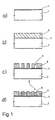
- FIG. 1 shows in a schematic sequence the process steps a) to h) for the production of three-dimensional, miniaturized electrode arrangements.
- an electroplating start layer 4 is applied to a flat carrier plate 2 after a cleaning step by sputtering.
- the carrier plate 2 can be made of Al 2 O 3 , in particular when the sensor to be produced is to be used in highly corrosive media, for example in exhaust gas diagnostics, to which platinum is applied as the electroplating start layer. If the requirements regarding corrosion resistance are lower, other substrates such as silicon or glass as well as metals such as gold, silver, copper, chromium and others can be used to produce the electroplating start layer. If the sensors are to be integrated with evaluation electronics, the use of silicon substrates is particularly advantageous.
- a photoresist layer 6 is then Example a photoresist, polyimide or a solid resist by spin coating (for liquid resist) or laminating (for solid resist) applied over the entire surface to the carrier plate 2.
- the layer thickness of the Photoresist layer 6 is in the liquid resist by the number of revolutions and for permanent resists by the number of laminated Resist layers set between 10 ⁇ m and 100 ⁇ m.
- the metallic to be produced is three-dimensional Electrode arrangement using a photolithographic mask transferred inversely into the photoresist layer 6.
- a photolithographic mask transferred inversely into the photoresist layer 6.
- the paint is applied directly via a process Mask exposed.
- Another possibility is on the photoresist to deposit an oxide, a nitride or metal, which is photolithographically structured as a mask for a dry etching process the photoresist layer 6 is used. Through the dry etching process smaller structure widths can be produced than with UV deep lithography Method. Both alternatives result in that Photoresist layer 6 lacquer trenches 8 are formed.
- step d) 8 metal is deposited in the lacquer trenches, wherein the lacquer trenches 8 can be filled up to their upper edge.
- the thickness of the metal layer 10 it is possible selectively adjust the sensor sensitivity.
- the choice of the departing Material is of the required corrosion resistance dependent on the sensor, so platinum, gold and silver for high Requirements and for lower requirements metals such as copper, Nickel or the like can be considered.
- the photoresist layer 6 is applied from the Metal structure 10 detached so that free three-dimensional electrode structures be preserved.
- the photoresist used can alkaline solutions, for example potassium hydroxide solution or organic solvents such as acetone are used.
- a heating electrode can be produced, to keep the sensor at a constant temperature.
- the geometry the heating electrode 10 ' is defined by a mask structure and the structuring as described in steps a) to e) carried out.
- step g) the electroplating layers 4 and 4 'are removed, to the conductive connections between the electrodes 10 of the Sensor and also the heater 10 'to interrupt.
- the electroplating start layers are eliminated by etching them off, for example by wet chemical etching, anionic etching or dry etching process.
- a paste is poured into the spaces between the electrodes 10 by means of the screen printing method, which paste is then applied to several hundred. Degree is sintered and forms the layer 14 containing the gas sensitive material.
- the paste is filled up to a certain height h, which is less than the depth T of the trenches or the three-dimensional electrodes 10.
- Further layers, for example protective layers, and a catalytically active layer are applied between the electrodes 10 above the gas-sensitive layer 14, as shown in FIG.
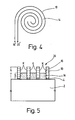
- the inner walls 16 of the electrodes 10, which are not covered by the gas-sensitive layer 14, can be used in particular when Platinum can be used as the electrode material for catalysis K, as shown in FIG. 5.
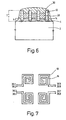
- FIGS. 2 to 4 and 7 to 9 show schematically preferred top view of electrode arrangements, which effectively covers the entire area of the sensor. Although the representation is two-dimensional, the electrode arrangements shown a three-dimensional shape. Structures with the same function have the same reference numbers Mistake.
- FIG. 2 shows a three-dimensional electrode arrangement with four-pole geometry are four individual electrodes 18, 20, 22 and 24 that accordingly allow four-pole measurements.
- the Four-pole measurement offers compared to two-pole measurement the advantage that contact resistance occurs measured and thus eliminated can.
- the Electrodes 18, 20, 22 and 24 for effective use of space be coiled, the condition being must be observed that only ever face the same electrodes. Otherwise would leakage currents occur which affect the sensor sensitivity reduce.
- Figure 2 shows an electrode arrangement in a meandering structure where the four electrodes 18, 20, 22 and 24 are contiguous are. In addition to this right-angled Any other electrode geometry can also be wound with curved or zigzag shaped Gradients provided according to the invention.
- FIG. 3 shows a three-dimensional electrode arrangement of electrodes 18 'and 20' in two-sequence geometry
- the electrodes are arranged in a meandering shape, whereby the electrodes run in a rectangular inner spiral shape.
- FIG. 4 shows a three-dimensional electrode arrangement of the Electrodes 18 'and 20' in two sequence geometry with a spiral electrode course represents.
- the electrode course can be on the lateral Heat distribution on the substrate can be adjusted so that the sensor area can be placed exactly on an isothermal surface.
- FIG. 5 illustrates that the filling height h of the gas sensitive Layer 14 less than the depth T of the enclosed by the electrodes 10 Trenches 26 is.
- the gas-sensitive material 14 uncovered inner walls 16 of the electrodes 10 are preferably especially when using platinum as electrode material, catalytically active.
- the gas to be detected is on the inner walls catalytically converted so that it is from the underlying gas sensitive Layer 14 can be detected.
- FIG. 6 illustrates an embodiment of the invention in which two further layers were applied to the gas-sensitive layer.
- the gas-sensitive layer 14 filled up to the height h is from a layer 28 covered, the catalytic conversion of the to Detecting gas is used, so that this is detected in the layer 14 can be.
- a protective or cover layer 30 is arranged, the underlying Layers 28 and 14 from external influences such as moisture and protects dirt.
- the three-dimensional electrode arrangement serves here, therefore, as a holding structure for the catalytically active layer 28 and the top layer 30.
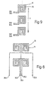
- Figure 7 shows the summary of three-dimensional miniaturized Electrode arrangements in a 2x2 area.
- the single electrodes are designated with 30.1 to 30.8.
- FIG. 8 shows the summary of a three-dimensional electrode arrangement to a quad structure with a center tap, which is carried out in a spiral arrangement.
- the four Individual sensors spatially resolved, d. H. be operated in such a way that, for example Influences of a gas flow can be compensated.
- other electrode arrangements are cloverleaf-shaped Structure in any geometry, for example as round and elliptical spirals, possible.
- FIG. 9 illustrates the arrangement of individual sensors along of a defined temperature gradient T. This embodiment enables temperature-dependent measurements by individually querying the sensors.
- the temperature gradient T is determined by the heater on the back fixed on the carrier plate 2.
- the formation of the sensor arrays shown in FIGS. 7 to 9 is particularly due to the three-dimensional structuring enabled miniaturization. Through the Arrays of arrays can take spatially resolved measurements and also the detection of different gases the use of several gas sensitive substances be made possible.
Landscapes
- Chemical & Material Sciences (AREA)
- Analytical Chemistry (AREA)
- Electrochemistry (AREA)
- Physics & Mathematics (AREA)
- Health & Medical Sciences (AREA)
- Life Sciences & Earth Sciences (AREA)
- Chemical Kinetics & Catalysis (AREA)
- Biochemistry (AREA)
- General Health & Medical Sciences (AREA)
- General Physics & Mathematics (AREA)
- Immunology (AREA)
- Pathology (AREA)
- Investigating Or Analyzing Materials By The Use Of Electric Means (AREA)
- Investigating Or Analyzing Materials By The Use Of Fluid Adsorption Or Reactions (AREA)
Description
Bereiche der dreidimensionalen Elektrodenanordnung als Wandkatalysator zu verwenden. Insbesondere wirkt die dreidimensionale Struktur der Elektrodenanordnung als Haltestruktur für diese Schichten und sie gewährleistet einen stabilen Aufbau des Sensorelementes. In den erfindungsgemäßen Ausführungsformen, in denen die Innenwände, also die die Gräben bildenden Wände, der dreidimensionalen Elektrodenanordnung nicht vollständig mit den genannten, das gassensitive Material überdeckenden Schichten bedeckt sind, können die Innenwände als Wandkatalysator verwendet werden. Die Verwendung einer das gassensitive Material überdeckenden katalytischen Schicht zusammen mit der Verwendung der Innenwände der dreidimensionalen Elektrodenanordnung als Wandkatalysator ist insbesondere dann vorteilhaft, wenn das gas-sensitive Material keine vollständige Selektivität für das messende Gas aufweist. In einem solchen Fall ist es besonders wünschenswert, das zu untersuchende Gasgemisch einer Katalyse zu unterziehen, wobei das zu detektierende Gas katalytisch so umgewandelt wird, dass es von der gassensitiven Schicht erkannt und möglichst selektiv bestimmt wird. Erfindungsgemäß wird eine verbesserte Selektivität der Gasmessung im gassensitiven Material durch Verwendung der katalytisch wirkenden Schicht oder durch deren Einsatz zusammen mit der Wandkatalyse erreicht.
- Figur 1
- schematisch die Abfolge der Verfahrensschritte zur Herstellung dreidimensionaler Elektrodenanordnungen, wobei das Sensorelement noch ohne die katalytisch wirkende Schicht im Längsschnitt dargestellt ist;
- Figur 2
- schematisch in zweidimensionaler Darstellung eine mäanderförmige, dreidimensionale Vierpol-Elektrodenanordnung;
- Figur 3
- schematisch in zweidimensionaler Darstellung eine rechteckförmige, dreidimensionale Zweipol-Elektrodenanordnung;
- Figur 4
- schematisch in zweidimensionaler Darstellung eine spiralförmige, dreidimensionale Zweipol-Elektrodenanordnung;
- Figur 5
- schematisch die Verwendung von Innenwände der im Längsschnitt dargestellten, dreidimensionalen Elektrodenanordnung zur Wandkatalyse, wobei das Sensorelement noch ohne die katalytisch wirkende Schicht dargestellt ist;
- Figur 6
- schematisch die Verwendung der im Längsschnitt dargestellten, dreidimensionalen Elektrodenanordnung als Haltestruktur für Katalysator- und Schutzschichten;
- Figur 7
- einen Sensorarray in 2x2-Anordnung;
- Figur 8
- einen Sensorarray in einer kleeblattförmigen Anordnung und
- Figur 9
- einen Sensorarray für temperaturabhängige Messungen in einer dritten Anordnung.
Platin als Elektrodenmaterial zur Katalyse K verwendet werden, wie in Figur 5 dargestellt.
Claims (11)
- Sensorelement mit mindestens einer auf einer Trägerplatte (2) aufgebrachten dreidimensionalen, Gräben (26) einer bestimmten Tiefe (T) bildenden Elektrodenanordnung zur Messung von Potentialen, Kapazitäts- und/oder Leitfähigkeitsänderungen in einer in einer bestimmten Höhe (h) in den Gräben (26) angeordneten gassensitiven Schicht (14), wobei die Höhe (h) der gassensitiven Schicht (14) geringer als die Tiefe (T) der Gräben (26) ist, dadurch gekennzeichnet, dass die gassensitive Schicht (14) von einer katalytisch wirkenden Schicht (28) bedeckt ist, und dass die Tiefe der Gräben (26) zwischen 10 µm und 100 µm liegt.
- Sensorelement nach Anspruch 1, dadurch gekennzeichnet, dass die gassensitive Schicht (14) nur in den Gräben (26) angeordnet ist.
- Sensorelement nach einem der Ansprüche 1 oder 2, dadurch gekennzeichnet, dass in den Gräben (26) über der gassensitiven Schicht (14) oder katalytisch wirkenden Schicht (28) eine Schutzschicht (30) angeordnet ist.
- Sensorelement nach einem der Ansprüche 1 bis 3, dadurch gekennzeichnet, dass die Elektroden (10) in Form einer Interdigitalstruktur angeordnet sind.
- Sensorelement nach einem der Ansprüche 1 bis 4, dadurch gekennzeichnet, dass die Elektrodenanordnung aus vier Einzelelektroden (18, 20, 22, 24) gebildet ist, die eine Vierpolmessung erlauben.
- Sensorelement nach einem der Ansprüche 1 bis 5, dadurch gekennzeichnet, dass die Trägerplatte (2) aus keramischem Material, Glas, Aluminiumoxid oder einem Silizium/Siliziumoxid-Gemisch besteht oder dieses enthält.
- Sensorelement nach einem der Ansprüche 1 bis 6, dadurch gekennzeichnet, dass die Elektroden (10) aus Platin, Gold, Silber, Kupfer oder Nickel bestehen oder dieses enthalten.
- Sensorarray umfassend mindestens zwei der Sensorelemente nach einem der Ansprüche 1 bis 7.
- Elektrochemischer Messfühler zur Bestimmung von Gaskonzentrationen umfassend ein Sensorelement oder ein Sensorarray nach einem der vorhergehenden Ansprüche.
- Verfahren zur Herstellung eines Sensorelementes mit dreidimensionaler Elektrodenanordnung, insbesondere eines Sensorelementes nach einem der Ansprüche 1 bis 7, wobei eine Galvanikstartschicht (4) auf einer Trägerplatte (2) abgeschieden, ein Photoresist (6) mit einer Dicke von 10 µm bis 100 µm auf der Galvanikstartschicht (4) aufgetragen, der Photoresist (6) strukturiert, dabei erzeugte Lackgräben (8) galvanisch bis zu einer definierten Höhe aufgefüllt, der Photoresist (6) entfernt, die Galvanikstartschicht (4) in den durch das Entfernen des Photoresists (6) entstandenen Elektrodengräben (26) einer bestimmten Tiefe (T) weggeätzt und zunächst gassensitives Material (14) in die Elektrodengräben (26) bis zu einer bestimmten Höhe (h) aufgefüllt wird, und wobei danach in den Elektrodengräben (26) ein katalytisch wirkendes Material (28) auf das gassensitive Material (14) aufgebracht wird.
- Verfahren nach Anspruch 10, dadurch gekennzeichnet, dass eine Heizelektrode (10) auf der Rückseite (12) der Trägerplatte (2) hergestellt wird.
Applications Claiming Priority (3)
| Application Number | Priority Date | Filing Date | Title |
|---|---|---|---|
| DE19642453 | 1996-10-15 | ||
| DE19642453A DE19642453C2 (de) | 1996-10-15 | 1996-10-15 | Anordnung für Gassensorelektroden |
| PCT/DE1997/002356 WO1998016819A1 (de) | 1996-10-15 | 1997-10-15 | Anordnung für gassensorelektroden |
Publications (2)
| Publication Number | Publication Date |
|---|---|
| EP0932828A1 EP0932828A1 (de) | 1999-08-04 |
| EP0932828B1 true EP0932828B1 (de) | 2003-01-15 |
Family
ID=7808777
Family Applications (1)
| Application Number | Title | Priority Date | Filing Date |
|---|---|---|---|
| EP97912051A Expired - Lifetime EP0932828B1 (de) | 1996-10-15 | 1997-10-15 | Anordnung für gassensorelektroden |
Country Status (6)
| Country | Link |
|---|---|
| US (1) | US6325979B1 (de) |
| EP (1) | EP0932828B1 (de) |
| JP (1) | JP3926395B2 (de) |
| KR (1) | KR100495462B1 (de) |
| DE (2) | DE19642453C2 (de) |
| WO (1) | WO1998016819A1 (de) |
Families Citing this family (96)
| Publication number | Priority date | Publication date | Assignee | Title |
|---|---|---|---|---|
| US9155496B2 (en) | 1997-03-04 | 2015-10-13 | Dexcom, Inc. | Low oxygen in vivo analyte sensor |
| US20050033132A1 (en) | 1997-03-04 | 2005-02-10 | Shults Mark C. | Analyte measuring device |
| US8527026B2 (en) | 1997-03-04 | 2013-09-03 | Dexcom, Inc. | Device and method for determining analyte levels |
| US6001067A (en) | 1997-03-04 | 1999-12-14 | Shults; Mark C. | Device and method for determining analyte levels |
| US7192450B2 (en) | 2003-05-21 | 2007-03-20 | Dexcom, Inc. | Porous membranes for use with implantable devices |
| US7657297B2 (en) * | 2004-05-03 | 2010-02-02 | Dexcom, Inc. | Implantable analyte sensor |
| US6862465B2 (en) | 1997-03-04 | 2005-03-01 | Dexcom, Inc. | Device and method for determining analyte levels |
| US7899511B2 (en) | 2004-07-13 | 2011-03-01 | Dexcom, Inc. | Low oxygen in vivo analyte sensor |
| US9066695B2 (en) | 1998-04-30 | 2015-06-30 | Abbott Diabetes Care Inc. | Analyte monitoring device and methods of use |
| US8688188B2 (en) | 1998-04-30 | 2014-04-01 | Abbott Diabetes Care Inc. | Analyte monitoring device and methods of use |
| US6175752B1 (en) | 1998-04-30 | 2001-01-16 | Therasense, Inc. | Analyte monitoring device and methods of use |
| US6949816B2 (en) | 2003-04-21 | 2005-09-27 | Motorola, Inc. | Semiconductor component having first surface area for electrically coupling to a semiconductor chip and second surface area for electrically coupling to a substrate, and method of manufacturing same |
| US8465425B2 (en) | 1998-04-30 | 2013-06-18 | Abbott Diabetes Care Inc. | Analyte monitoring device and methods of use |
| US8974386B2 (en) | 1998-04-30 | 2015-03-10 | Abbott Diabetes Care Inc. | Analyte monitoring device and methods of use |
| US8480580B2 (en) | 1998-04-30 | 2013-07-09 | Abbott Diabetes Care Inc. | Analyte monitoring device and methods of use |
| US8346337B2 (en) | 1998-04-30 | 2013-01-01 | Abbott Diabetes Care Inc. | Analyte monitoring device and methods of use |
| DE19859998C2 (de) * | 1998-12-23 | 2000-11-30 | Siemens Ag | Gassensor und Verfahren zu dessen Herstellung |
| DE20004229U1 (de) | 2000-03-07 | 2000-05-04 | Fraunhofer-Gesellschaft zur Förderung der angewandten Forschung e.V., 80636 München | Sauerstoffgassensor |
| US6468407B2 (en) * | 2000-12-19 | 2002-10-22 | Delphi Technologies, Inc. | NOx reduction sensor coating |
| US6560471B1 (en) | 2001-01-02 | 2003-05-06 | Therasense, Inc. | Analyte monitoring device and methods of use |
| EP1397068A2 (de) | 2001-04-02 | 2004-03-17 | Therasense, Inc. | Gerät und verfahren zur blutzuckerverfolgung |
| US20030032874A1 (en) | 2001-07-27 | 2003-02-13 | Dexcom, Inc. | Sensor head for use with implantable devices |
| US6702857B2 (en) | 2001-07-27 | 2004-03-09 | Dexcom, Inc. | Membrane for use with implantable devices |
| US7179421B1 (en) * | 2002-01-24 | 2007-02-20 | Sandia Corporation | Multi-pin chemiresistors for microchemical sensors |
| US9282925B2 (en) | 2002-02-12 | 2016-03-15 | Dexcom, Inc. | Systems and methods for replacing signal artifacts in a glucose sensor data stream |
| US10022078B2 (en) | 2004-07-13 | 2018-07-17 | Dexcom, Inc. | Analyte sensor |
| US9247901B2 (en) | 2003-08-22 | 2016-02-02 | Dexcom, Inc. | Systems and methods for replacing signal artifacts in a glucose sensor data stream |
| US8010174B2 (en) | 2003-08-22 | 2011-08-30 | Dexcom, Inc. | Systems and methods for replacing signal artifacts in a glucose sensor data stream |
| US8260393B2 (en) | 2003-07-25 | 2012-09-04 | Dexcom, Inc. | Systems and methods for replacing signal data artifacts in a glucose sensor data stream |
| US7613491B2 (en) | 2002-05-22 | 2009-11-03 | Dexcom, Inc. | Silicone based membranes for use in implantable glucose sensors |
| US8364229B2 (en) | 2003-07-25 | 2013-01-29 | Dexcom, Inc. | Analyte sensors having a signal-to-noise ratio substantially unaffected by non-constant noise |
| US7226978B2 (en) | 2002-05-22 | 2007-06-05 | Dexcom, Inc. | Techniques to improve polyurethane membranes for implantable glucose sensors |
| TWI237112B (en) * | 2003-09-03 | 2005-08-01 | Hon Hai Prec Ind Co Ltd | Gas sensor |
| US7134999B2 (en) | 2003-04-04 | 2006-11-14 | Dexcom, Inc. | Optimized sensor geometry for an implantable glucose sensor |
| US7112304B2 (en) * | 2003-04-11 | 2006-09-26 | Therm-O-Disc, Incorporated | Robust chemiresistor sensor |
| US7875293B2 (en) | 2003-05-21 | 2011-01-25 | Dexcom, Inc. | Biointerface membranes incorporating bioactive agents |
| WO2005010518A1 (en) * | 2003-07-23 | 2005-02-03 | Dexcom, Inc. | Rolled electrode array and its method for manufacture |
| WO2005012873A2 (en) | 2003-07-25 | 2005-02-10 | Dexcom, Inc. | Electrode systems for electrochemical sensors |
| US9763609B2 (en) | 2003-07-25 | 2017-09-19 | Dexcom, Inc. | Analyte sensors having a signal-to-noise ratio substantially unaffected by non-constant noise |
| US7108778B2 (en) * | 2003-07-25 | 2006-09-19 | Dexcom, Inc. | Electrochemical sensors including electrode systems with increased oxygen generation |
| WO2007120442A2 (en) | 2003-07-25 | 2007-10-25 | Dexcom, Inc. | Dual electrode system for a continuous analyte sensor |
| US7494465B2 (en) | 2004-07-13 | 2009-02-24 | Dexcom, Inc. | Transcutaneous analyte sensor |
| US8060173B2 (en) | 2003-08-01 | 2011-11-15 | Dexcom, Inc. | System and methods for processing analyte sensor data |
| US8160669B2 (en) | 2003-08-01 | 2012-04-17 | Dexcom, Inc. | Transcutaneous analyte sensor |
| US7774145B2 (en) | 2003-08-01 | 2010-08-10 | Dexcom, Inc. | Transcutaneous analyte sensor |
| US8761856B2 (en) | 2003-08-01 | 2014-06-24 | Dexcom, Inc. | System and methods for processing analyte sensor data |
| US8676287B2 (en) | 2003-08-01 | 2014-03-18 | Dexcom, Inc. | System and methods for processing analyte sensor data |
| US8275437B2 (en) | 2003-08-01 | 2012-09-25 | Dexcom, Inc. | Transcutaneous analyte sensor |
| US20190357827A1 (en) | 2003-08-01 | 2019-11-28 | Dexcom, Inc. | Analyte sensor |
| US7920906B2 (en) | 2005-03-10 | 2011-04-05 | Dexcom, Inc. | System and methods for processing analyte sensor data for sensor calibration |
| US20140121989A1 (en) | 2003-08-22 | 2014-05-01 | Dexcom, Inc. | Systems and methods for processing analyte sensor data |
| US9247900B2 (en) | 2004-07-13 | 2016-02-02 | Dexcom, Inc. | Analyte sensor |
| US8532730B2 (en) | 2006-10-04 | 2013-09-10 | Dexcom, Inc. | Analyte sensor |
| US8364231B2 (en) | 2006-10-04 | 2013-01-29 | Dexcom, Inc. | Analyte sensor |
| US8423114B2 (en) | 2006-10-04 | 2013-04-16 | Dexcom, Inc. | Dual electrode system for a continuous analyte sensor |
| US11633133B2 (en) | 2003-12-05 | 2023-04-25 | Dexcom, Inc. | Dual electrode system for a continuous analyte sensor |
| ATE480761T1 (de) | 2003-12-05 | 2010-09-15 | Dexcom Inc | Kalibrationsmethoden für einen kontinuierlich arbeitenden analytsensor |
| US8287453B2 (en) | 2003-12-05 | 2012-10-16 | Dexcom, Inc. | Analyte sensor |
| US7637868B2 (en) | 2004-01-12 | 2009-12-29 | Dexcom, Inc. | Composite material for implantable device |
| JP4460000B2 (ja) * | 2004-03-31 | 2010-04-28 | エージェンシー フォー サイエンス,テクノロジー アンド リサーチ | 試験材料のガス透過率を測定するためのセンサ |
| US8792955B2 (en) | 2004-05-03 | 2014-07-29 | Dexcom, Inc. | Transcutaneous analyte sensor |
| GB2417083B (en) * | 2004-08-13 | 2006-08-16 | Mark Sinclair Varney | An electrochemical carbon dioxide gas sensor |
| US20060015020A1 (en) * | 2004-07-06 | 2006-01-19 | Dexcom, Inc. | Systems and methods for manufacture of an analyte-measuring device including a membrane system |
| US8989833B2 (en) | 2004-07-13 | 2015-03-24 | Dexcom, Inc. | Transcutaneous analyte sensor |
| US8452368B2 (en) | 2004-07-13 | 2013-05-28 | Dexcom, Inc. | Transcutaneous analyte sensor |
| US8565848B2 (en) | 2004-07-13 | 2013-10-22 | Dexcom, Inc. | Transcutaneous analyte sensor |
| US8886272B2 (en) | 2004-07-13 | 2014-11-11 | Dexcom, Inc. | Analyte sensor |
| US7783333B2 (en) | 2004-07-13 | 2010-08-24 | Dexcom, Inc. | Transcutaneous medical device with variable stiffness |
| JP2006064410A (ja) * | 2004-08-24 | 2006-03-09 | Denso Corp | オイル劣化検出装置 |
| JP4115482B2 (ja) | 2005-02-22 | 2008-07-09 | 日本特殊陶業株式会社 | ガスセンサ |
| US20090076360A1 (en) | 2007-09-13 | 2009-03-19 | Dexcom, Inc. | Transcutaneous analyte sensor |
| US8133178B2 (en) | 2006-02-22 | 2012-03-13 | Dexcom, Inc. | Analyte sensor |
| WO2007048736A1 (en) * | 2005-10-26 | 2007-05-03 | Inergy Automotive Systems Research (Societe Anonyme) | Capacitive gauge comprising interdigital electrodes on an insulating substrate |
| WO2007048777A1 (en) * | 2005-10-26 | 2007-05-03 | Inergy Automotive Systems Research (Societe Anonyme) | Capacitive gauge |
| FR2892509B1 (fr) * | 2005-10-26 | 2007-12-21 | Inergy Automotive Systems Res | Jauge capacitive pour reservoir a carburant |
| EP1971510B1 (de) * | 2006-01-10 | 2010-10-13 | Guardian Industries Corp. | Regensensor mit sigma-delta-modulation und/oder footprint-vergleich(en) |
| US9371032B2 (en) | 2006-01-10 | 2016-06-21 | Guardian Industries Corp. | Moisture sensor and/or defogger with Bayesian improvements, and related methods |
| US7492270B2 (en) * | 2006-01-10 | 2009-02-17 | Guardian Industries Corp. | Rain sensor with sigma-delta modulation and/or footprinting comparison(s) |
| GB2434647A (en) * | 2006-01-13 | 2007-08-01 | Asthma Alert Ltd | Gas Concentration and Humidity Sensor |
| US9757061B2 (en) | 2006-01-17 | 2017-09-12 | Dexcom, Inc. | Low oxygen in vivo analyte sensor |
| EP1991110B1 (de) | 2006-03-09 | 2018-11-07 | DexCom, Inc. | Systeme und verfahren zur aufbereitung von analytensensordaten |
| US20070295082A1 (en) * | 2006-06-06 | 2007-12-27 | Honeywell International Inc. | Flow sensor transducer with dual spiral wheatstone bridge elements |
| US7920907B2 (en) | 2006-06-07 | 2011-04-05 | Abbott Diabetes Care Inc. | Analyte monitoring system and method |
| US7831287B2 (en) | 2006-10-04 | 2010-11-09 | Dexcom, Inc. | Dual electrode system for a continuous analyte sensor |
| JP4913866B2 (ja) * | 2007-04-10 | 2012-04-11 | 北陸電気工業株式会社 | 感応センサ及びその製造方法 |
| US20200037875A1 (en) | 2007-05-18 | 2020-02-06 | Dexcom, Inc. | Analyte sensors having a signal-to-noise ratio substantially unaffected by non-constant noise |
| US8417312B2 (en) | 2007-10-25 | 2013-04-09 | Dexcom, Inc. | Systems and methods for processing sensor data |
| US8396528B2 (en) | 2008-03-25 | 2013-03-12 | Dexcom, Inc. | Analyte sensor |
| JP2010048627A (ja) * | 2008-08-20 | 2010-03-04 | Sumitomo Electric Ind Ltd | ガスセンサおよびその製造方法 |
| US9149220B2 (en) | 2011-04-15 | 2015-10-06 | Dexcom, Inc. | Advanced analyte sensor calibration and error detection |
| US11371951B2 (en) | 2012-09-27 | 2022-06-28 | Sensirion Ag | Gas sensor comprising a set of one or more sensor cells |
| US8802568B2 (en) * | 2012-09-27 | 2014-08-12 | Sensirion Ag | Method for manufacturing chemical sensor with multiple sensor cells |
| TWI515429B (zh) * | 2014-03-12 | 2016-01-01 | 友達光電股份有限公司 | 化學感測器及其製造方法 |
| EP2952885B1 (de) * | 2014-06-02 | 2016-07-27 | Sensirion AG | Gassensor |
| CN109983328B (zh) | 2016-11-23 | 2022-03-18 | 罗伯特·博世有限公司 | 气体传感器和用于探测气体的方法 |
| CN112034012B (zh) * | 2020-05-19 | 2024-04-23 | 北京机械设备研究所 | Mems气体传感器气敏单元及制备方法 |
Family Cites Families (8)
| Publication number | Priority date | Publication date | Assignee | Title |
|---|---|---|---|---|
| JP2829416B2 (ja) | 1989-07-28 | 1998-11-25 | 株式会社クラベ | 感ガス素子 |
| JPH0572163A (ja) * | 1990-11-30 | 1993-03-23 | Mitsui Mining Co Ltd | 半導体式ガスセンサー |
| US5252949A (en) * | 1991-08-28 | 1993-10-12 | Hughes Aircraft Company | Chemical sensor for carbon monoxide detection |
| DE4137030A1 (de) * | 1991-11-11 | 1993-05-13 | Mst Micro Sensor Tech Gmbh | Elektrochemischer sensor zur messung der gaskonzentration |
| GB9405899D0 (en) * | 1994-03-24 | 1994-05-11 | Pima Sensors Inc | Gas sensor and sensing device |
| US5560810A (en) * | 1995-03-16 | 1996-10-01 | Sem Corporation | Electrochemical gas sensor assembly |
| US5698771A (en) * | 1995-03-30 | 1997-12-16 | The United States Of America As Represented By The United States National Aeronautics And Space Administration | Varying potential silicon carbide gas sensor |
| US5841021A (en) * | 1995-09-05 | 1998-11-24 | De Castro; Emory S. | Solid state gas sensor and filter assembly |
-
1996
- 1996-10-15 DE DE19642453A patent/DE19642453C2/de not_active Expired - Fee Related
-
1997
- 1997-10-15 US US09/284,661 patent/US6325979B1/en not_active Expired - Fee Related
- 1997-10-15 EP EP97912051A patent/EP0932828B1/de not_active Expired - Lifetime
- 1997-10-15 DE DE59709166T patent/DE59709166D1/de not_active Expired - Lifetime
- 1997-10-15 JP JP51791298A patent/JP3926395B2/ja not_active Expired - Fee Related
- 1997-10-15 KR KR10-1999-7003237A patent/KR100495462B1/ko not_active Expired - Fee Related
- 1997-10-15 WO PCT/DE1997/002356 patent/WO1998016819A1/de not_active Ceased
Also Published As
| Publication number | Publication date |
|---|---|
| EP0932828A1 (de) | 1999-08-04 |
| KR100495462B1 (ko) | 2005-06-16 |
| US6325979B1 (en) | 2001-12-04 |
| DE59709166D1 (de) | 2003-02-20 |
| JP2001502060A (ja) | 2001-02-13 |
| JP3926395B2 (ja) | 2007-06-06 |
| WO1998016819A1 (de) | 1998-04-23 |
| DE19642453C2 (de) | 1998-07-23 |
| DE19642453A1 (de) | 1998-04-16 |
| KR20000049146A (ko) | 2000-07-25 |
Similar Documents
| Publication | Publication Date | Title |
|---|---|---|
| EP0932828B1 (de) | Anordnung für gassensorelektroden | |
| DE10359173B4 (de) | Messvorrichtung mit mehreren auf einem Substrat angeordneten potentiometrischen Elektrodenpaaren | |
| DE3817905C2 (de) | ||
| DE4424342C1 (de) | Sensorarray | |
| DE10049901C2 (de) | Vorrichtung und Verfahren zur elektrisch beschleunigten Immobilisierung und zur Detektion von Molekülen | |
| DE69814318T2 (de) | Festelektrolyt mit innerer Referenzkammer und Elektroden auf Innen- und Aussenflächen | |
| DE112005000168T5 (de) | Verfahren zur Herstellung eines Kunstharzformgehäuses, Alkoholkonzentrationssensor und Vorrichtung zum Messen einer Alkoholkonzentration | |
| DE19941420A1 (de) | Elektrischer Widerstand mit wenigstens zwei Anschlußkontaktfeldern auf einem Substrat mit wenigstens einer Ausnehmung sowie Verfahren zu dessen Herstellung | |
| DE10133466A1 (de) | Schichtverbund und mikromechanisches Sensorelement, insbesondere Gassensorelement, mit diesem Schichtverbund | |
| EP0377792A1 (de) | Sensor zur Bestimmung der Gaskonzentration in einem Gasgemisch durch Messung der Wärmetönung | |
| EP0446483A2 (de) | Katalytischer Gassensor | |
| DE19649366C2 (de) | Mikrosensor zur Flüssigkeitsanalyse, insbesondere von Alkohol-Benzin-Gemischen | |
| EP1272671A2 (de) | Biosensor, biosensor-array, verfahren zum herstellen einer elektrode eines biosensors, verfahren zum herstellen eines biosensors | |
| DE4110653C2 (de) | Thermoelektrischer Wandler, Verfahren zu dessen Herstellung sowie dessen Verwendung | |
| EP0645621A2 (de) | Sensoranordnung | |
| EP1471349B1 (de) | Potentiometrische Sensoreinrichtung für pH-Wertmessung | |
| DE4334410C3 (de) | Dünnschicht-Gassensor | |
| EP0366687B1 (de) | Herstellung von inerten, katalytisch wirksamen oder gassensitiven keramikschichten für gassensoren | |
| DE102009020743A1 (de) | Fotolithographisch strukturierter Dickschichtsensor | |
| WO2006058882A1 (de) | Biochemisches halbleiterchiplabor mit angekoppeltem adressier- und steuerchip und verfahren zur herstellung desselben | |
| DE10211358B4 (de) | Vertikal-Impedanz-Sensor-Anordnung und Verfahren zum Herstellen einer Vertikal-Impedanz-Sensor-Anordnung | |
| DE10315190A1 (de) | Gassensor | |
| DE68923699T2 (de) | Dünnfilmfeuchtigkeitprüfelemente und verfahren zur herstellung. | |
| EP3513166B1 (de) | Sensorelement zur erfassung von partikeln eines messgases in einem messgasraum | |
| DE4244223A1 (de) | Sensor zur Bestimmung von Bestandteilen von Gasgemischen |
Legal Events
| Date | Code | Title | Description |
|---|---|---|---|
| PUAI | Public reference made under article 153(3) epc to a published international application that has entered the european phase |
Free format text: ORIGINAL CODE: 0009012 |
|
| 17P | Request for examination filed |
Effective date: 19990517 |
|
| AK | Designated contracting states |
Kind code of ref document: A1 Designated state(s): CH DE FR GB LI |
|
| 17Q | First examination report despatched |
Effective date: 20010510 |
|
| GRAG | Despatch of communication of intention to grant |
Free format text: ORIGINAL CODE: EPIDOS AGRA |
|
| GRAG | Despatch of communication of intention to grant |
Free format text: ORIGINAL CODE: EPIDOS AGRA |
|
| GRAH | Despatch of communication of intention to grant a patent |
Free format text: ORIGINAL CODE: EPIDOS IGRA |
|
| GRAH | Despatch of communication of intention to grant a patent |
Free format text: ORIGINAL CODE: EPIDOS IGRA |
|
| GRAA | (expected) grant |
Free format text: ORIGINAL CODE: 0009210 |
|
| AK | Designated contracting states |
Kind code of ref document: B1 Designated state(s): CH DE FR GB LI |
|
| REG | Reference to a national code |
Ref country code: GB Ref legal event code: FG4D Free format text: NOT ENGLISH Ref country code: CH Ref legal event code: EP |
|
| REF | Corresponds to: |
Ref document number: 59709166 Country of ref document: DE Date of ref document: 20030220 Kind code of ref document: P |
|
| RBV | Designated contracting states (corrected) |
Designated state(s): CH DE FR GB IT LI |
|
| RBV | Designated contracting states (corrected) |
Designated state(s): CH DE FR GB IT LI |
|
| REG | Reference to a national code |
Ref country code: CH Ref legal event code: NV Representative=s name: SCINTILLA AG, DIREKTION |
|
| GBT | Gb: translation of ep patent filed (gb section 77(6)(a)/1977) |
Effective date: 20030425 |
|
| ET | Fr: translation filed | ||
| PLBE | No opposition filed within time limit |
Free format text: ORIGINAL CODE: 0009261 |
|
| STAA | Information on the status of an ep patent application or granted ep patent |
Free format text: STATUS: NO OPPOSITION FILED WITHIN TIME LIMIT |
|
| 26N | No opposition filed |
Effective date: 20031016 |
|
| PGFP | Annual fee paid to national office [announced via postgrant information from national office to epo] |
Ref country code: GB Payment date: 20041005 Year of fee payment: 8 |
|
| PGFP | Annual fee paid to national office [announced via postgrant information from national office to epo] |
Ref country code: CH Payment date: 20041025 Year of fee payment: 8 |
|
| PG25 | Lapsed in a contracting state [announced via postgrant information from national office to epo] |
Ref country code: GB Free format text: LAPSE BECAUSE OF NON-PAYMENT OF DUE FEES Effective date: 20051015 |
|
| PG25 | Lapsed in a contracting state [announced via postgrant information from national office to epo] |
Ref country code: LI Free format text: LAPSE BECAUSE OF NON-PAYMENT OF DUE FEES Effective date: 20051031 Ref country code: CH Free format text: LAPSE BECAUSE OF NON-PAYMENT OF DUE FEES Effective date: 20051031 |
|
| REG | Reference to a national code |
Ref country code: CH Ref legal event code: PL |
|
| GBPC | Gb: european patent ceased through non-payment of renewal fee |
Effective date: 20051015 |
|
| PGFP | Annual fee paid to national office [announced via postgrant information from national office to epo] |
Ref country code: IT Payment date: 20081029 Year of fee payment: 12 |
|
| PGFP | Annual fee paid to national office [announced via postgrant information from national office to epo] |
Ref country code: FR Payment date: 20081021 Year of fee payment: 12 |
|
| REG | Reference to a national code |
Ref country code: FR Ref legal event code: ST Effective date: 20100630 |
|
| PG25 | Lapsed in a contracting state [announced via postgrant information from national office to epo] |
Ref country code: FR Free format text: LAPSE BECAUSE OF NON-PAYMENT OF DUE FEES Effective date: 20091102 |
|
| PG25 | Lapsed in a contracting state [announced via postgrant information from national office to epo] |
Ref country code: IT Free format text: LAPSE BECAUSE OF NON-PAYMENT OF DUE FEES Effective date: 20091015 |
|
| PGFP | Annual fee paid to national office [announced via postgrant information from national office to epo] |
Ref country code: DE Payment date: 20101217 Year of fee payment: 14 |
|
| PG25 | Lapsed in a contracting state [announced via postgrant information from national office to epo] |
Ref country code: DE Free format text: LAPSE BECAUSE OF NON-PAYMENT OF DUE FEES Effective date: 20120501 |
|
| REG | Reference to a national code |
Ref country code: DE Ref legal event code: R119 Ref document number: 59709166 Country of ref document: DE Effective date: 20120501 |