EP0932909B1 - Procede de connexion d'emetteurs de champ en fibres et cathodes emettrices de champ fabriquees a partir desdits emetteurs - Google Patents
Procede de connexion d'emetteurs de champ en fibres et cathodes emettrices de champ fabriquees a partir desdits emetteurs Download PDFInfo
- Publication number
- EP0932909B1 EP0932909B1 EP97910027A EP97910027A EP0932909B1 EP 0932909 B1 EP0932909 B1 EP 0932909B1 EP 97910027 A EP97910027 A EP 97910027A EP 97910027 A EP97910027 A EP 97910027A EP 0932909 B1 EP0932909 B1 EP 0932909B1
- Authority
- EP
- European Patent Office
- Prior art keywords
- field emission
- substrate
- fiber
- emission fiber
- metal ribbon
- Prior art date
- Legal status (The legal status is an assumption and is not a legal conclusion. Google has not performed a legal analysis and makes no representation as to the accuracy of the status listed.)
- Expired - Lifetime
Links
- 239000000835 fiber Substances 0.000 title claims abstract description 154
- 238000000034 method Methods 0.000 title claims abstract description 18
- 239000000758 substrate Substances 0.000 claims abstract description 107
- 229910052751 metal Inorganic materials 0.000 claims abstract description 61
- 239000002184 metal Substances 0.000 claims abstract description 61
- 230000006835 compression Effects 0.000 claims abstract description 6
- 238000007906 compression Methods 0.000 claims abstract description 6
- PCHJSUWPFVWCPO-UHFFFAOYSA-N gold Chemical compound [Au] PCHJSUWPFVWCPO-UHFFFAOYSA-N 0.000 claims description 11
- 239000010931 gold Substances 0.000 claims description 11
- 229910052737 gold Inorganic materials 0.000 claims description 11
- 229910052782 aluminium Inorganic materials 0.000 claims description 3
- XAGFODPZIPBFFR-UHFFFAOYSA-N aluminium Chemical compound [Al] XAGFODPZIPBFFR-UHFFFAOYSA-N 0.000 claims description 3
- 229910000838 Al alloy Inorganic materials 0.000 claims description 2
- 229910003460 diamond Inorganic materials 0.000 description 30
- 239000010432 diamond Substances 0.000 description 30
- OKTJSMMVPCPJKN-UHFFFAOYSA-N Carbon Chemical compound [C] OKTJSMMVPCPJKN-UHFFFAOYSA-N 0.000 description 27
- 239000000463 material Substances 0.000 description 16
- 229910052799 carbon Inorganic materials 0.000 description 14
- 229910002804 graphite Inorganic materials 0.000 description 13
- 239000010439 graphite Substances 0.000 description 13
- 239000002131 composite material Substances 0.000 description 9
- 239000011162 core material Substances 0.000 description 9
- 239000013078 crystal Substances 0.000 description 9
- 229910021397 glassy carbon Inorganic materials 0.000 description 9
- 239000000725 suspension Substances 0.000 description 7
- OAICVXFJPJFONN-UHFFFAOYSA-N Phosphorus Chemical compound [P] OAICVXFJPJFONN-UHFFFAOYSA-N 0.000 description 6
- VYZAMTAEIAYCRO-UHFFFAOYSA-N Chromium Chemical compound [Cr] VYZAMTAEIAYCRO-UHFFFAOYSA-N 0.000 description 5
- 229910052804 chromium Inorganic materials 0.000 description 5
- 239000011651 chromium Substances 0.000 description 5
- 238000000576 coating method Methods 0.000 description 5
- 239000004020 conductor Substances 0.000 description 5
- WFKWXMTUELFFGS-UHFFFAOYSA-N tungsten Chemical compound [W] WFKWXMTUELFFGS-UHFFFAOYSA-N 0.000 description 5
- 229910052721 tungsten Inorganic materials 0.000 description 5
- 239000010937 tungsten Substances 0.000 description 5
- ZOKXTWBITQBERF-UHFFFAOYSA-N Molybdenum Chemical compound [Mo] ZOKXTWBITQBERF-UHFFFAOYSA-N 0.000 description 4
- 239000011248 coating agent Substances 0.000 description 4
- 229910052750 molybdenum Inorganic materials 0.000 description 4
- 239000011733 molybdenum Substances 0.000 description 4
- 239000005361 soda-lime glass Substances 0.000 description 4
- RYGMFSIKBFXOCR-UHFFFAOYSA-N Copper Chemical compound [Cu] RYGMFSIKBFXOCR-UHFFFAOYSA-N 0.000 description 3
- KFZMGEQAYNKOFK-UHFFFAOYSA-N Isopropanol Chemical compound CC(C)O KFZMGEQAYNKOFK-UHFFFAOYSA-N 0.000 description 3
- 229910052802 copper Inorganic materials 0.000 description 3
- 239000010949 copper Substances 0.000 description 3
- 238000005530 etching Methods 0.000 description 3
- 150000002739 metals Chemical class 0.000 description 3
- 238000003825 pressing Methods 0.000 description 3
- IJGRMHOSHXDMSA-UHFFFAOYSA-N Atomic nitrogen Chemical compound N#N IJGRMHOSHXDMSA-UHFFFAOYSA-N 0.000 description 2
- 229920000271 Kevlar® Polymers 0.000 description 2
- -1 i.e. Substances 0.000 description 2
- 239000012212 insulator Substances 0.000 description 2
- 239000004973 liquid crystal related substance Substances 0.000 description 2
- 238000001878 scanning electron micrograph Methods 0.000 description 2
- 229910052710 silicon Inorganic materials 0.000 description 2
- 239000010703 silicon Substances 0.000 description 2
- XLYOFNOQVPJJNP-UHFFFAOYSA-N water Chemical compound O XLYOFNOQVPJJNP-UHFFFAOYSA-N 0.000 description 2
- RZVAJINKPMORJF-UHFFFAOYSA-N Acetaminophen Chemical compound CC(=O)NC1=CC=C(O)C=C1 RZVAJINKPMORJF-UHFFFAOYSA-N 0.000 description 1
- 229920000049 Carbon (fiber) Polymers 0.000 description 1
- 239000004677 Nylon Substances 0.000 description 1
- 238000001069 Raman spectroscopy Methods 0.000 description 1
- XUIMIQQOPSSXEZ-UHFFFAOYSA-N Silicon Chemical compound [Si] XUIMIQQOPSSXEZ-UHFFFAOYSA-N 0.000 description 1
- RTAQQCXQSZGOHL-UHFFFAOYSA-N Titanium Chemical compound [Ti] RTAQQCXQSZGOHL-UHFFFAOYSA-N 0.000 description 1
- 238000004873 anchoring Methods 0.000 description 1
- 239000004917 carbon fiber Substances 0.000 description 1
- 239000007833 carbon precursor Substances 0.000 description 1
- 239000000919 ceramic Substances 0.000 description 1
- 239000008367 deionised water Substances 0.000 description 1
- 229910021641 deionized water Inorganic materials 0.000 description 1
- 230000008021 deposition Effects 0.000 description 1
- 239000003599 detergent Substances 0.000 description 1
- 230000005684 electric field Effects 0.000 description 1
- 230000001747 exhibiting effect Effects 0.000 description 1
- 238000005242 forging Methods 0.000 description 1
- 239000007789 gas Substances 0.000 description 1
- 239000011521 glass Substances 0.000 description 1
- 239000002241 glass-ceramic Substances 0.000 description 1
- 238000000608 laser ablation Methods 0.000 description 1
- 238000004519 manufacturing process Methods 0.000 description 1
- 229910052757 nitrogen Inorganic materials 0.000 description 1
- 229920001778 nylon Polymers 0.000 description 1
- 229910052698 phosphorus Inorganic materials 0.000 description 1
- 239000011574 phosphorus Substances 0.000 description 1
- 229920000728 polyester Polymers 0.000 description 1
- 239000002243 precursor Substances 0.000 description 1
- 239000005297 pyrex Substances 0.000 description 1
- 238000005488 sandblasting Methods 0.000 description 1
- 238000004626 scanning electron microscopy Methods 0.000 description 1
- HBMJWWWQQXIZIP-UHFFFAOYSA-N silicon carbide Chemical compound [Si+]#[C-] HBMJWWWQQXIZIP-UHFFFAOYSA-N 0.000 description 1
- 229910010271 silicon carbide Inorganic materials 0.000 description 1
- 229910052719 titanium Inorganic materials 0.000 description 1
- 239000010936 titanium Substances 0.000 description 1
- 230000000007 visual effect Effects 0.000 description 1
Images


Classifications
-
- H—ELECTRICITY
- H01—ELECTRIC ELEMENTS
- H01J—ELECTRIC DISCHARGE TUBES OR DISCHARGE LAMPS
- H01J9/00—Apparatus or processes specially adapted for the manufacture, installation, removal, maintenance of electric discharge tubes, discharge lamps, or parts thereof; Recovery of material from discharge tubes or lamps
- H01J9/02—Manufacture of electrodes or electrode systems
-
- H—ELECTRICITY
- H01—ELECTRIC ELEMENTS
- H01J—ELECTRIC DISCHARGE TUBES OR DISCHARGE LAMPS
- H01J1/00—Details of electrodes, of magnetic control means, of screens, or of the mounting or spacing thereof, common to two or more basic types of discharge tubes or lamps
- H01J1/02—Main electrodes
- H01J1/30—Cold cathodes, e.g. field-emissive cathode
- H01J1/304—Field-emissive cathodes
-
- B—PERFORMING OPERATIONS; TRANSPORTING
- B82—NANOTECHNOLOGY
- B82Y—SPECIFIC USES OR APPLICATIONS OF NANOSTRUCTURES; MEASUREMENT OR ANALYSIS OF NANOSTRUCTURES; MANUFACTURE OR TREATMENT OF NANOSTRUCTURES
- B82Y10/00—Nanotechnology for information processing, storage or transmission, e.g. quantum computing or single electron logic
-
- H—ELECTRICITY
- H01—ELECTRIC ELEMENTS
- H01J—ELECTRIC DISCHARGE TUBES OR DISCHARGE LAMPS
- H01J9/00—Apparatus or processes specially adapted for the manufacture, installation, removal, maintenance of electric discharge tubes, discharge lamps, or parts thereof; Recovery of material from discharge tubes or lamps
- H01J9/02—Manufacture of electrodes or electrode systems
- H01J9/022—Manufacture of electrodes or electrode systems of cold cathodes
-
- H—ELECTRICITY
- H01—ELECTRIC ELEMENTS
- H01J—ELECTRIC DISCHARGE TUBES OR DISCHARGE LAMPS
- H01J9/00—Apparatus or processes specially adapted for the manufacture, installation, removal, maintenance of electric discharge tubes, discharge lamps, or parts thereof; Recovery of material from discharge tubes or lamps
- H01J9/02—Manufacture of electrodes or electrode systems
- H01J9/022—Manufacture of electrodes or electrode systems of cold cathodes
- H01J9/025—Manufacture of electrodes or electrode systems of cold cathodes of field emission cathodes
Definitions
- This invention relates to a method for connecting, both electrically and mechanically, an electrically conducting field emission fiber to an electrically conducting area of a substrate, an improved fibrous cathode and an improved flat panel display containing such a fibrous cathode.
- Display panels are used in a wide variety of applications such as home and commercial televisions, laptop and desktop computers and indoor and outdoor advertising and information presentations.
- Flat panel displays are only a few inches thick in contrast to the deep cathode ray tube monitors found on most televisions and desktop computers.
- Flat panel displays are a necessity for laptop computers, but also provide advantages in weight and size for many of the other applications.
- Currently laptop computer flat panel displays use liquid crystals which can be switched from a transparent state to an opaque one by the application of small electrical signals. It is difficult to reliably produce these displays in sizes larger than that suitable for laptop computers.
- Plasma displays have been proposed as an alternative to liquid crystal displays.
- a plasma display uses tiny pixel cells of electrically charged gases to produce an image and requires relatively large electrical voltages and power to operate.
- a cathode comprised of fibrous electron field emitters, wherein the fibers lie essentially in the plane of the cathode and emission is achieved at desired regions along the length of the fiber, have advantages over previously disclosed cathodes.
- the fibrous cathode is supported by a substrate and further improved performance is achieved when the portions of the fibrous cathode addressed, and from which electron emission occurs, are suspended and not in direct physical contact with the substrate.
- the invention provides a method for connecting, both mechanically and electrically, an electrically conducting field emission fiber to an electrically conducting area of a substrate , comprising:
- the metal ribbon is gold, aluminum or an aluminum alloy.
- the length of the metal ribbon is not critical. However, it must be sufficiently long to contour over the field emission fiber and have adequate portions on both sides of the field emission fiber to allow connection to the substrate.
- the width of the metal ribbon is from about 2 mil (0.05 mm) to about 40 mil (1 mm) and the thickness is from about 0.25 mil (0.006 mm) to about 2 mil (0.05 mm).
- the invention also provides an improved fibrous cathode comprised of at least one field emission fiber and a substrate, characterized in that an electrically conducting field emission fiber is connected, both mechanically and electrically, to an electrically conducting area of a substrate by a metal ribbon located over said field emission fiber with the dimension along the length of said metal ribbon essentially perpendicular to the axis of said field emission fiber such that said metal ribbon extends over said field emission fiber with each end portion of said metal ribbon in direct contact with said area of said substrate, the metal ribbon being bonded to the electrically conducting area of the substrate and to the field emission fiber.
- the invention provides an improved flat panel display containing such a fibrous cathode.
- the field emission fiber is connected to the cathode substrate at multiple places along the length of the field emission fiber.
- An important advantage of this method of connecting a field emission fiber to a substrate is that it can be used in an automatic process in which a multitude of such connections can be readily made.
- the present invention provides a method for connecting a field emission fiber to a substrate and thereby provides an improved fibrous cathode.
- fibrous cathode embraces a cathode formed of at least one field emission fiber.
- a flat panel display containing such a fibrous cathode is also improved.
- the flat panel display comprises (a) a fibrous cathode formed of at least one field emission fiber supported on a substrate, (b) an optically transparent electrically conductive film serving as an anode and spaced apart from the fibrous cathode, and (c) a phosphor layer, immediately adjacent to the anode, capable of emitting light upon bombardment by electrons emitted by the fibers.
- the improvement comprises the connection of the field emission fiber to the substrate by the method of this invention. It will be understood that the arrangement of the anode and the phosphor layer may vary.
- the phosphor layer may be positioned between the anode and the cathode or, alternatively, the anode may be positioned between the phosphor layer and the cathode.
- the flat panel display can also contain one or more gate electrodes situated between the anode and the cathode.
- Flat panel displays are so-called because they are only a few inches thick. They are generally planar but can be curved or have other configurations as required by the specific application. Thus, as used herein, the terms “display panel” or “flat panel display” embrace planar and curved surfaces as well as other possible geometries.
- the field emitter or field emission material used in the fibrous cathode of this invention is a field emission electron source.
- Various fiber geometries are possible in forming the fibrous cathode which is comprised of at least one such fiber.
- fiber is meant one dimension substantially greater than the other two dimensions.
- the fibers can have any shape fiber cross-section, limited only by the design of the spinneret. Fibers may be bundled together in the fashion of multiple filaments.
- These fibers can be made of the field emitter alone (e.g., graphite fibers) or can be a composite fiber of a non-field emitter core with a thin layer of field emitter surrounding the core.
- the core material is conductive or semiconductive.
- the fiber may consist of a more complex core structure, for example, a non-conductive core surrounded by a thin coating of conductive or semiconductive material with a field emission material surrounding the coating.
- connection method of this invention can be used with any field emission material.
- Diamond, diamond-like carbon or glassy carbon may be employed as the field emission material.
- the fibrous cathode can then be comprised of diamond, diamond-like carbon or glassy carbon composite fibers consisting essentially of diamond, diamond-like carbon or glassy carbon on'non-diamond core fibers.
- the core material can be, e.g., a conductive carbon such as graphite or a metal such as tungsten, copper, titanium or molybdenum or can be, e.g., silicon or silicon carbide.
- the core can be a metallized insulator such as tungsten coated on a non-conductive polyester, nylon or Kevlar® fiber (Kevlar® is a registered trademark of E. I. du Pont de Nemours and Company, Wilmington, DE).
- a diamond, diamond-like carbon or glassy carbon precursor can be coated onto the non-diamond core and the diamond, diamond-like carbon or glassy carbon is then formed by appropriate treatment of the precursor.
- the axis of each fiber of which the fibrous cathode is comprised lies essentially in the plane of the cathode.
- electron emission from these fibers occurs along the length of the fibers utilized and not from the fiber tip or end.
- Diamond fibers and fibrous diamond composites such as diamond-coated graphite or diamond-coated carbon preferably include a sub-micron scale crystal structure of diamond, i.e., diamond having crystal sizes of generally less than about 1 micron in at least one crystal dimension.
- such diamond crystals include at least some exposed 111-oriented crystal facets, some exposed 100-oriented crystal facets, or some of both.
- Another form of diamond having suitable sub-micron dimensions is commonly referred to as cauliflower-diamond which has fine grained balls as opposed to a pyramidal structure.
- Fibers including diamond-like carbon with an appropriate short range order may also provide for field emission materials with high current densities.
- short range order is generally meant an ordered arrangement of atoms less than about 10 nanometers (nm) in any dimension. It may also be possible to use fibers, e.g., carbon fibers, coated with amorphic diamond via laser ablation as described by Davanloo et al. in J. Mater. Res., Vol. 5, No. 11, Nov. 1990.
- Fibers containing glassy carbon, an amorphous material exhibiting Raman peaks at about 1380 cm-1 and 1598 cm-1, as the field emitter material are also useful.
- “Diamond-like carbon” is used herein to designate the material referred to in the literature as diamond-like carbon as well as glassy carbon and carbon containing microscopic inclusions of glassy carbon, all of which are diamond-like in their performance as fiber field emission materials.
- the composite fibers have a total diameter ranging from about 1 micron to about 200 microns.
- the diamond layer or coating in such a composite fiber can generally be from about 50 Angstroms (5 nm) to about 50,000 Angstroms (5 ⁇ m), preferably from about 1000 Angstroms (0.1 ⁇ m) to about 20,000 Angstroms (2 ⁇ m), more preferably from about 1000 Angstroms (0.1 ⁇ m) to about 5,000 (0.5 ⁇ m) Angstroms.
- Diamond typically has several low index facets of low or negative electron affinity, e.g., 100-faceted diamond with a low affinity whereas 111-faceted diamond has a negative electron affinity.
- Diamond-like carbon or glassy carbon may preferably be n-type doped with, e.g., nitrogen or phosphorus, to provide more electrons and reduce the work function of the material.
- Such a diamond or diamond-like carbon layer preferably has rough jagged edges such that a series of spikes and valleys is present upon the diamond or diamond-like carbon layer.
- this surface morphology results from a microcrystalline structure of the diamond material. It may be preferred that a minor amount of graphite be situated between at least a portion of said diamond crystals within said diamond coating for best results. It may also be preferred that diamond grown via CVD develop in columnar fashion due to slight misalignment between the growing crystals. This misalignment may also promote the development of the rough jagged edges of the diamond morphology.
- the field emission fiber is supported on a substrate to provide a fibrous cathode.
- the substrate may be flat or may be undulating with one or more sets of regularly spaced parallel rows of crests and valleys. (See, e.g., WO 95/22169 for illustrations and more detail.)
- the substrate is flat the whole length of each field emission fiber is in contact with the substrate.
- a field emission fiber may be aligned along the length of each valley of the undulating surface again resulting in the whole length of each field emission fiber being in contact with the substrate. It can be advantageous to deposit an electrically conducting film on the area of the substrate which is in contact with the field emission fiber.
- strips of electrically conducting film corresponding to the rows of fibers can be deposited.
- an electrically conducting film can be deposited along the length of each valley of the undulating surface before placing the composite fibers in the valleys.
- Metals such as copper, gold, chromium, molybdenum, and tungsten can be used. Such films provide electron reservoirs for the electron emission composite fibers and also enable the emission composite fibers in each valley to be addressed individually if desired.
- a fibrous cathode and a flat panel display comprised of a fibrous cathode is improved when the portions of the fibrous cathode addressed, and from which electron emission occurs, are suspended and not in direct physical contact with the substrate.
- Suspension of the field emission fiber can be accomplished in a number of ways. When the substrate is flat the field emission fiber can be suspended above the surface of the substrate on stand-offs or pedestals.
- Undulating substrates can be especially useful in achieving suspended portions of the field emission fiber.
- the undulating portion comprises a regularly undulating surface on the substrate consisting of parallel rows of valleys and essentially flat crests.
- the fibrous cathode consists essentially of a regularly spaced parallel array of fibers, wherein the fibers are supported on the essentially flat crests of the substrate and suspended above the valleys of the substrate.
- the undulating surface can formed by etching a smooth substrate such that the essentially flat crests correspond to lightly etched regions of the substrate and the valleys correspond to more heavily etched regions of the substrate.
- the fibers of the fibrous cathode are essentially perpendicular to the parallel rows of valleys and essentially flat crests. It is also preferable to have the substrate coated with a continuous strip of an electrically conductive material in the valleys and on the sides of the valleys of the set of parallel rows of valleys and essentially flat crests but not along the essentially flat crests. This thereby provides a substrate coated with a parallel array of continuous strips of electrically conductive material, one such strip along each row of valleys. This parallel array serves as a gate electrode.
- a variation of this embodiment which can provide better control of the electron emission is one in which the valleys and the essentially flat crests occur in rows but these rows are not continuous, i.e., there is a region of the substrate along which the surface is undulating with a succession of valleys and essentially flat crests and on either side of this region are regions with essentially flat surfaces and on the other sides of both these flat regions are other regions along which the surface is undulating with a succession of valleys and essentially flat crests.
- valleys and essentially flat crests there are still parallel rows of valleys and essentially flat crests; however they are not continuous rows but rather rows of valleys with the valleys placed at regular intervals along each row and rows of essentially flat crests with the essentially flat crests placed at regular intervals along each row.
- Figures 1(a), 1(b) and 1(c) Such an embodiment in which the undulating surface is formed by etching is shown in Figures 1(a), 1(b) and 1(c).
- Figure 1(a) shows an etch pattern on the surface of the substrate. This pattern could be used to form the valleys and essentially flat crests.
- Figure 1(b) shows the areas of the substrate that would be etched and
- Figure 1(c) shows the depth profile along the 21-22 line of Figure 1(b).
- the fibers of the fibrous cathode would be aligned along lines such as the 21-22 line of Figure 1(b).
- metals such as copper, gold, chromium, molybdenum, and tungsten can be used and such films provide electron reservoirs for the electron emission composite fibers and enable electrical contact to be made at
- an undulating substrate to suspend the field emission fiber involves a substrate which contains two sets of parallel rows of crests and valleys.
- the first set of parallel crests and valleys provide the valleys along which the fibrous cathode consisting essentially of at least one fiber is aligned.
- the second set of parallel crests and valleys is preferably perpendicular to the first set.
- the walls between the crests and valleys can be vertical. Sloped or curved sections can also be used.
- the parallel rows of crests and valleys are shown regularly spaced, i.e., the distance between the centers of two neighboring crests or between the centers of two neighboring valleys is the same within each set.
- each triad i.e., each set of three pair of crests and valleys, will be regularly spaced.
- the valleys of the second set are typically narrower and less deep than the valleys of the first set.
- the valleys of the first set are from about 25 ⁇ m to about 250 ⁇ m deep and from about 10 ⁇ m to about 350 ⁇ m wide and the crests of the first set are from about 25 ⁇ m to about 250 ⁇ m wide.
- the valleys of the second set are from about 10 ⁇ m to about 150 ⁇ m deep and from about 50 ⁇ m to about 125 ⁇ m wide and the crests of the second set are from about 600 ⁇ m to about 700 ⁇ m wide.
- Typical ways of forming two such sets of parallel rows of crests and valleys on these substrate materials are etching, using ceramic GREEN TAPETM (commercially available from E. I. du Pont de Nemours and Company, Wilmington, DE), sandblasting, thick film sequential deposition and forging.
- the valleys of the second set provide the means of suspending the fibrous cathode.
- the fibrous cathode can be placed along the length of each valley of the first set and be suspended by the surfaces of the valleys of the second set when these valleys are less deep than those of the first set.
- a suspension element is disposed along the length of each of the valleys of the second set to support the fibrous cathode.
- the suspension element can be a continuous structure, e.g., a non-emission fiber aligned along the length of each valley and upon which the emission fibrous cathode rests. A film extended along the length of each valley could also be used.
- the substrate coated with an electrically conductive material Before the fibrous cathode is positioned on the substrate, it is preferable to have the substrate coated with an electrically conductive material to provide means to apply a voltage to the fiber and create the electric field necessary for emission.
- the electrically conductive material coats the substrate except in the valleys and on the sides of the valleys of the second set thereby providing a substrate coated with a parallel array of continuous strips of electrically conductive material. This parallel array serves as a gate electrode.
- a non-emission fiber aligned along the length of each of the valleys of the second set on top of said fibrous cathode thereby anchoring said fibrous cathode in place can be used when suspension is by means of a non-emission fiber or means other than a non-emission fiber.
- the suspension element can be a discontinuous structure comprised of a series of pedestals or films on each valley of the second set at each intersection with a valley of the first set.
- the use of a suspension element is required when the valleys of the second set are as deep or deeper than the valleys of the first set.
- the substrate can be made of insulators such as soda lime glass, Pyrex, and glass ceramics.
- a metal film on the substrate can serve as the substrate contact area for the connection.
- bonding the metal ribbon to the substrate embraces directly bonding the metal ribbon to the substrate as well as bonding the metal ribbon to a film, layer or other structured material deposited on or attached to the substrate.
- the field emission fiber For both flat and undulating substrates, the field emission fiber must be attached mechanically to the substrate and further there must be provision for making electrical contact to the field emission fiber. Typically such connections would be made at each end of the field emission fiber.
- This invention provides a method for connecting the field emission fiber to the substrate by means of a metal ribbon.
- metal ribbon is used to describe a ribbon of material with electrical, mechanical and thermal properties similar to those of metals such as gold and aluminum.
- the field emission fiber is placed on the substrate and centered over the area where the connection is to be made.
- the metal ribbon is placed over and in direct contact with the field emission fiber.
- the dimension along the length of the metal ribbon is essentially perpendicular to the axis of the field emission fiber and the metal ribbon extends over the field emission fiber with each end portion of the metal ribbon in direct contact with the substrate. As a result, the field emission fiber is held firmly against the substrate.
- the metal ribbon is typically about 2 mil (0.05 mm) to about 40 mil (1 mm) wide and about 0.25 mil (0.006 mm) to about 2 mil (0.05 mm) thick.
- the length of the metal ribbon is not critical; however, it must be sufficiently long to surround and envelope or contour the field emission fiber and to provide an adequate portion of metal ribbon on either side of the field emission fiber to allow connection to the substrate. Ultrasonic, thermocompression or compression bonding is used to bond each end portion of the metal ribbon to the substrate and to bond the portion of the ribbon directly contoured around the field emission fiber to the field emission fiber.
- the method of this invention can be used to attach the field emission fiber to a substrate at positions intermediate to the two ends of the field emission fiber.
- Such connections can provide both mechanical and electrical advantages. It has been observed that the field emission fiber, and particularly the portion of the field emission fiber that is addressed and from which electron emission occurs, sometimes moves when being addressed. Such movement negatively affects the performance of the fibrous cathode. Intermediate connections will restrict such movement. Intermediate connections will also hold the field emission fiber in place during fabrication of the cathode assembly of the fibrous cathode and of the flat panel display.
- the method of this invention is useful to provide intermediate connections along the length of the field emission fiber. It may be advantageous to create a flattened region on the substrate where the connections are to be made to provide better connections.
- connections can be made along the field emission fiber at places which are intermediate to the regions of the field emission fiber which are addressed and from which electron emission occurs.
- connections can be made at the places on the substrate or suspension elements on the substrate from which the field emission fiber is suspended.
- the connections can be made at positions along line C of Figure 1(c) where the field emission fibers intersect line C and other corresponding positions along the field emission fibers.
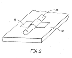
- Figure 2 shows a field emission fiber 31 on a substrate 32 .
- the metal ribbon 33 is shown placed over and in direct contact with the field emission fiber.
- the metal ribbon is contoured to the shape of the field emission fiber to better hold it to the substrate.
- the end portions of the metal ribbon on either side of the field emission fiber are bonded to the substrate and the portion of the metal ribbon directly contoured around the field emission fiber is bonded to the field emission fiber by ultrasonic, thermocompression or compression bonding.
- Ultrasonic bonding is achieved by firmly pressing the metal ribbon between the bonding tool and the substrate or field emission fiber to which it is to be bonded and supplying a burst of ultrasonic energy usually at a frequency of about 60 kHz.
- the combination of the pressure and the ultrasonic energy results in a metallurgical weld between the metal ribbon and the substrate or to the field emission fiber.
- the temperature of the substrate may be elevated to facilitate the interdiffusion. This combination of providing pressure and thermal and ultrasonic energy is sometimes referred to as thermosonic bonding.
- ultrasonic bonding embraces bonding in which the metal ribbon is firmly pressed between the bonding tool and the substrate or field emission fiber to which it is to be bonded and a burst of ultrasonic energy is supplied no matter whether the temperature of the metal ribbon and the substrate or field emission fiber is ambient or elevated.
- Thermocompression bonding can be accomplished by applying pressure to the region of the metal ribbon that is in contact with the substrate or that which is in contact with the field emission fiber to provide the necessary intimate contact and simultaneously raising the temperature of those same regions.
- the temperature must be elevated to temperatures of the order of 370 to 380°C.
- Compression bonding can be accomplished by applying pressure to a region of the metal ribbon that is in contact with the substrate or that which is in contact with the field emission fiber. Pressures needed are higher than in the other bonding techniques. Care must be taken in bonding to the field emission fiber.
- the substrate comprised of soda lime glass, a layer of chromium and a layer of gold upon which the field emission fiber would be placed, was prepared as follows.
- a soda lime glass substrate was cleaned with a detergent (Sparkleen® commercially available from Fisher Scientific) and rinsed well in deionized water. The water was removed in an isopropyl alcohol vapor drier.
- One side of the glass was coated with a 50 nm layer of chromium in the form of a series of circles each about 1 mm in diameter.
- a 200 nm layer of gold was deposited onto the chromium. The gold film would serve as the substrate contact area.
- a graphite fiber with a diameter of 7 ⁇ m was placed on one of the gold contact areas of the substrate and positioned such that it was centered over the contact area.
- a piece of gold ribbon approximately 10 mil (250 ⁇ m) long, approximately 5 mil (125 ⁇ m) wide and 0.5 mil (13 ⁇ m) thick was placed over the graphite fiber at the contact area. This ribbon was centered over the graphite fiber. As a result, the graphite fiber is sandwiched between the contact area on the substrate and the metal ribbon.
- the substrate was heated to a temperature of 85°C.
- the metal ribbon was then bonded to the substrate and to the graphite fiber using a Kulicke and Soffa, Model #422, ultrasonic wire bonder. Each time a force of about 10 g was applied with the bonder and ultrasonic energy was applied for 1/4 second. This resulted in the graphite fiber being mechanically and electrically connected to the substrate.
- FIGS. 3(a) and 3(b) show scanning electron micrographs, at different magnifications, wherein the graphite fiber is attached to the substrate by the metal ribbon.
- the places at which the ultrasonic bonder was used are readily seen. In commercial practice, bonding could be made to take place in a continuous manner instead of in a series of individual hits.
Landscapes
- Engineering & Computer Science (AREA)
- Manufacturing & Machinery (AREA)
- Chemical & Material Sciences (AREA)
- Nanotechnology (AREA)
- Physics & Mathematics (AREA)
- Mathematical Physics (AREA)
- Theoretical Computer Science (AREA)
- Crystallography & Structural Chemistry (AREA)
- Cathode-Ray Tubes And Fluorescent Screens For Display (AREA)
- Electrodes For Cathode-Ray Tubes (AREA)
- Cold Cathode And The Manufacture (AREA)
Abstract
Claims (7)
- Procédé de connexion, à la fois mécanique et électrique, d'une fibre d'émission de champ électroconductrice (31) à une zone électroconductrice d'un substrat (32), comprenant:(a) la mise en place de ladite fibre d'émission de champ (31) sur la surface dudit substrat (32) et le centrage de la fibre d'émission de champ (31) sur ladite zone dudit substrat (32), là où une connexion est à réaliser;(b) la mise en place d'un ruban métallique (33) sur ladite fibre d'émission de champ (31), la dimension le long de la longueur dudit ruban métallique (33) étant essentiellement perpendiculaire à l'axe de ladite fibre d'émission de champ (31), et le placement étant tel que ledit ruban métallique (33) se prolonge sur ladite fibre d'émission de champ (31), avec chaque portion d'extrémité dudit ruban métallique (33) en contact direct avec ladite zone dudit substrat (32); et(c) la liaison dudit ruban métallique (33) à ladite zone dudit substrat (32) et à ladite fibre d'émission de champ (31) par l'intermédiaire d'un procédé de liaison aux ultrasons, d'un procédé de liaison par thermocompression ou d'un procédé de liaison par compression.
- Procédé selon la revendication 1, dans lequel ledit ruban métallique (33) est lié audit substrat (32) et à ladite fibre d'émission de champ (31) par un procédé de liaison aux ultrasons.
- Procédé selon la revendication 1, dans lequel ledit ruban métallique (33) est l'or, l'aluminium ou un alliage d'aluminium.
- Cathode fibreuse améliorée, constituée d'au moins une fibre d'émission de champ (31) et d'un substrat (32), caractérisée en ce qu'une fibre d'émission de champ (31) électroconductrice est connectée, à la fois mécaniquement et électriquement, à une zone électroconductrice d'un substrat (32) par un ruban métallique (33), situé sur ladite fibre d'émission de champ (31), la dimension le long de la longueur dudit ruban métallique (33) étant essentiellement perpendiculaire à l'axe de ladite fibre d'émission de champ (31), de telle manière que ledit ruban métallique (33) se prolonge sur ladite fibre d'émission de champ (31), avec chaque portion d'extrémité dudit ruban métallique (33) en contact direct avec ladite zone dudit substrat (32), le ruban métallique (33) étant lié à la zone électroconductrice du substrat (32) et à la fibre d'émission de champ (31).
- Cathode fibreuse améliorée selon la revendication 4, dans laquelle ladite fibre d'émission de champ (31) est connectée aux zones électroconductrices dudit substrat (32) à des emplacement multiples le long de la longueur de ladite fibre d'émission de champ (31).
- Affichage à écran plat amélioré contenant la cathode fibreuse améliorée de la revendication 4.
- Affichage à écran plat amélioré contenant la cathode fibreuse améliorée de la revendication 5.
Applications Claiming Priority (3)
| Application Number | Priority Date | Filing Date | Title |
|---|---|---|---|
| US2867796P | 1996-10-17 | 1996-10-17 | |
| US28677P | 1996-10-17 | ||
| PCT/US1997/018180 WO1998016943A1 (fr) | 1996-10-17 | 1997-10-06 | Procede de connexion d'emetteurs de champ en fibres et cathodes emettrices de champ fabriquees a partir desdits emetteurs |
Publications (2)
| Publication Number | Publication Date |
|---|---|
| EP0932909A1 EP0932909A1 (fr) | 1999-08-04 |
| EP0932909B1 true EP0932909B1 (fr) | 2004-09-22 |
Family
ID=21844835
Family Applications (1)
| Application Number | Title | Priority Date | Filing Date |
|---|---|---|---|
| EP97910027A Expired - Lifetime EP0932909B1 (fr) | 1996-10-17 | 1997-10-06 | Procede de connexion d'emetteurs de champ en fibres et cathodes emettrices de champ fabriquees a partir desdits emetteurs |
Country Status (9)
| Country | Link |
|---|---|
| US (1) | US6069435A (fr) |
| EP (1) | EP0932909B1 (fr) |
| JP (1) | JP3794711B2 (fr) |
| KR (1) | KR100471334B1 (fr) |
| CN (1) | CN1234134A (fr) |
| AU (1) | AU4750297A (fr) |
| DE (1) | DE69730851T2 (fr) |
| TW (1) | TW375752B (fr) |
| WO (1) | WO1998016943A1 (fr) |
Families Citing this family (7)
| Publication number | Priority date | Publication date | Assignee | Title |
|---|---|---|---|---|
| US9272371B2 (en) | 2013-05-30 | 2016-03-01 | Agc Automotive Americas R&D, Inc. | Solder joint for an electrical conductor and a window pane including same |
| US10263362B2 (en) | 2017-03-29 | 2019-04-16 | Agc Automotive Americas R&D, Inc. | Fluidically sealed enclosure for window electrical connections |
| US10849192B2 (en) | 2017-04-26 | 2020-11-24 | Agc Automotive Americas R&D, Inc. | Enclosure assembly for window electrical connections |
| KR102431255B1 (ko) * | 2017-10-18 | 2022-08-11 | 유니버시티 오브 센트럴 플로리다 리서치 파운데이션, 인코포레이티드 | 전기 전도성 코어 및 변색 코팅을 갖는 섬유 |
| US11479886B2 (en) | 2020-05-21 | 2022-10-25 | University Of Central Florida Research Foundation, Inc. | Color-changing fabric and applications |
| US11708649B2 (en) | 2020-05-21 | 2023-07-25 | University Of Central Florida Research Foundation, Inc. | Color-changing fabric having printed pattern |
| CN113990729B (zh) * | 2021-10-28 | 2023-06-06 | 郑州航空工业管理学院 | 一种准宏观冷场发射电子枪及其制造方法 |
Family Cites Families (12)
| Publication number | Priority date | Publication date | Assignee | Title |
|---|---|---|---|---|
| GB1394055A (en) * | 1971-07-09 | 1975-05-14 | Nat Res Dev | Electron emitters |
| US4055780A (en) * | 1975-04-10 | 1977-10-25 | National Institute For Researches In Inorganic Materials | Thermionic emission cathode having a tip of a single crystal of lanthanum hexaboride |
| JPS5659423A (en) * | 1980-10-16 | 1981-05-22 | Nec Home Electronics Ltd | Manufacture of frame electrode |
| US4728851A (en) * | 1982-01-08 | 1988-03-01 | Ford Motor Company | Field emitter device with gated memory |
| US4857799A (en) * | 1986-07-30 | 1989-08-15 | Sri International | Matrix-addressed flat panel display |
| US5015912A (en) * | 1986-07-30 | 1991-05-14 | Sri International | Matrix-addressed flat panel display |
| US5449970A (en) * | 1992-03-16 | 1995-09-12 | Microelectronics And Computer Technology Corporation | Diode structure flat panel display |
| CA2152472A1 (fr) * | 1992-12-23 | 1994-07-07 | Nalin Kumar | Ecran plat a triodes dote de cathodes a emission par effet de champ plates |
| AU5897594A (en) * | 1993-06-02 | 1994-12-20 | Microelectronics And Computer Technology Corporation | Amorphic diamond film flat field emission cathode |
| US5578901A (en) * | 1994-02-14 | 1996-11-26 | E. I. Du Pont De Nemours And Company | Diamond fiber field emitters |
| DE69608284T2 (de) * | 1995-08-14 | 2000-12-21 | E.I. Du Pont De Nemours And Co., Wilmington | Anzeigetafel unter verwendung von faserartigen feldeffektemittern |
| US5648699A (en) * | 1995-11-09 | 1997-07-15 | Lucent Technologies Inc. | Field emission devices employing improved emitters on metal foil and methods for making such devices |
-
1997
- 1997-10-06 EP EP97910027A patent/EP0932909B1/fr not_active Expired - Lifetime
- 1997-10-06 DE DE69730851T patent/DE69730851T2/de not_active Expired - Fee Related
- 1997-10-06 JP JP51842798A patent/JP3794711B2/ja not_active Expired - Fee Related
- 1997-10-06 KR KR10-1999-7003364A patent/KR100471334B1/ko not_active Expired - Fee Related
- 1997-10-06 WO PCT/US1997/018180 patent/WO1998016943A1/fr not_active Ceased
- 1997-10-06 AU AU47502/97A patent/AU4750297A/en not_active Abandoned
- 1997-10-06 US US09/284,646 patent/US6069435A/en not_active Expired - Fee Related
- 1997-10-06 CN CN97198886A patent/CN1234134A/zh active Pending
- 1997-11-22 TW TW086115318A patent/TW375752B/zh active
Also Published As
| Publication number | Publication date |
|---|---|
| CN1234134A (zh) | 1999-11-03 |
| JP3794711B2 (ja) | 2006-07-12 |
| EP0932909A1 (fr) | 1999-08-04 |
| KR100471334B1 (ko) | 2005-03-07 |
| DE69730851T2 (de) | 2005-09-22 |
| TW375752B (en) | 1999-12-01 |
| WO1998016943A1 (fr) | 1998-04-23 |
| KR20000049256A (ko) | 2000-07-25 |
| JP2001502466A (ja) | 2001-02-20 |
| DE69730851D1 (de) | 2004-10-28 |
| US6069435A (en) | 2000-05-30 |
| AU4750297A (en) | 1998-05-11 |
Similar Documents
| Publication | Publication Date | Title |
|---|---|---|
| EP0745265B1 (fr) | Emetteur de champ en fibre de diamant ou analogue ou en fibre de carbone vitreux | |
| JP4008123B2 (ja) | 炭素系超微細冷陰極及びその作製方法 | |
| KR100307042B1 (ko) | 비정질다이아몬드막플랫필드방출캐소드 | |
| KR100384092B1 (ko) | 전자방출장치의제조방법 | |
| CN100435262C (zh) | 电子发射元件、电子源和图像显示装置的制造方法 | |
| US6646282B1 (en) | Field emission display device | |
| EP0932909B1 (fr) | Procede de connexion d'emetteurs de champ en fibres et cathodes emettrices de champ fabriquees a partir desdits emetteurs | |
| US6825607B2 (en) | Field emission display device | |
| US20030042833A1 (en) | Method for activating nanotubes as field emission sources | |
| US20040007956A1 (en) | Field emission display device | |
| EP1164618B1 (fr) | Dispositif d'emission d'electrons et dispositif d'affichage d'images utilisant un dispositif d'emission d'electrons | |
| EP0845150B1 (fr) | Panneaux de visualisation faisant appel a des emetteurs par effets de champ a fibres | |
| US6750617B2 (en) | Field emission display device | |
| EP0861498B1 (fr) | Emetteurs de champ en suie de charbon recuite et cathodes d'emission de champ produites a partir de ce materiau | |
| US6750616B2 (en) | Field emission display device | |
| US7367860B2 (en) | Sintering method for carbon nanotube cathode of field-emission display | |
| US6121721A (en) | Unitary spacers for a display device | |
| JP3474142B2 (ja) | 電界放出型電子源アレイの製造方法、電界放出型電子源アレイ、及びその製造装置 | |
| JPH09166782A (ja) | 電界放出型表示素子のバックライトを持つ液晶表示装置 | |
| KR100260266B1 (ko) | 패널의 측면부 결함을 보상한 전계방출표시소자 및 그 구동방법 | |
| JP2005317304A (ja) | 電子放出素子の製造方法、および画像表示装置の製造方法、ならびに映像受信表示装置 |
Legal Events
| Date | Code | Title | Description |
|---|---|---|---|
| PUAI | Public reference made under article 153(3) epc to a published international application that has entered the european phase |
Free format text: ORIGINAL CODE: 0009012 |
|
| 17P | Request for examination filed |
Effective date: 19990319 |
|
| AK | Designated contracting states |
Kind code of ref document: A1 Designated state(s): DE FR GB |
|
| 17Q | First examination report despatched |
Effective date: 20020510 |
|
| GRAP | Despatch of communication of intention to grant a patent |
Free format text: ORIGINAL CODE: EPIDOSNIGR1 |
|
| RAP1 | Party data changed (applicant data changed or rights of an application transferred) |
Owner name: E.I. DU PONT DE NEMOURS AND COMPANY |
|
| GRAS | Grant fee paid |
Free format text: ORIGINAL CODE: EPIDOSNIGR3 |
|
| GRAA | (expected) grant |
Free format text: ORIGINAL CODE: 0009210 |
|
| AK | Designated contracting states |
Kind code of ref document: B1 Designated state(s): DE FR GB |
|
| REG | Reference to a national code |
Ref country code: GB Ref legal event code: FG4D |
|
| REF | Corresponds to: |
Ref document number: 69730851 Country of ref document: DE Date of ref document: 20041028 Kind code of ref document: P |
|
| RAP2 | Party data changed (patent owner data changed or rights of a patent transferred) |
Owner name: THE REGENTS OF THE UNIVERSITY OF CALIFORNIA |
|
| PLBE | No opposition filed within time limit |
Free format text: ORIGINAL CODE: 0009261 |
|
| STAA | Information on the status of an ep patent application or granted ep patent |
Free format text: STATUS: NO OPPOSITION FILED WITHIN TIME LIMIT |
|
| ET | Fr: translation filed | ||
| 26N | No opposition filed |
Effective date: 20050623 |
|
| PGFP | Annual fee paid to national office [announced via postgrant information from national office to epo] |
Ref country code: DE Payment date: 20071004 Year of fee payment: 11 |
|
| PGFP | Annual fee paid to national office [announced via postgrant information from national office to epo] |
Ref country code: GB Payment date: 20071003 Year of fee payment: 11 Ref country code: FR Payment date: 20071009 Year of fee payment: 11 |
|
| GBPC | Gb: european patent ceased through non-payment of renewal fee |
Effective date: 20081006 |
|
| REG | Reference to a national code |
Ref country code: FR Ref legal event code: ST Effective date: 20090630 |
|
| PG25 | Lapsed in a contracting state [announced via postgrant information from national office to epo] |
Ref country code: DE Free format text: LAPSE BECAUSE OF NON-PAYMENT OF DUE FEES Effective date: 20090501 |
|
| PG25 | Lapsed in a contracting state [announced via postgrant information from national office to epo] |
Ref country code: FR Free format text: LAPSE BECAUSE OF NON-PAYMENT OF DUE FEES Effective date: 20081031 |
|
| PG25 | Lapsed in a contracting state [announced via postgrant information from national office to epo] |
Ref country code: GB Free format text: LAPSE BECAUSE OF NON-PAYMENT OF DUE FEES Effective date: 20081006 |