EP0932935B1 - Abstimmsystem für empfänger - Google Patents
Abstimmsystem für empfänger Download PDFInfo
- Publication number
- EP0932935B1 EP0932935B1 EP98903240A EP98903240A EP0932935B1 EP 0932935 B1 EP0932935 B1 EP 0932935B1 EP 98903240 A EP98903240 A EP 98903240A EP 98903240 A EP98903240 A EP 98903240A EP 0932935 B1 EP0932935 B1 EP 0932935B1
- Authority
- EP
- European Patent Office
- Prior art keywords
- frequency
- tuning
- oscillator
- signal
- stepped
- Prior art date
- Legal status (The legal status is an assumption and is not a legal conclusion. Google has not performed a legal analysis and makes no representation as to the accuracy of the status listed.)
- Expired - Lifetime
Links
- 230000005540 biological transmission Effects 0.000 claims description 7
- 238000003786 synthesis reaction Methods 0.000 claims description 4
- 238000000034 method Methods 0.000 claims description 3
- 101150036282 Pfdn2 gene Proteins 0.000 claims description 2
- 102100024920 Prefoldin subunit 2 Human genes 0.000 claims description 2
- 101100243555 Saccharomyces cerevisiae (strain ATCC 204508 / S288c) GIM4 gene Proteins 0.000 claims description 2
- 230000015572 biosynthetic process Effects 0.000 claims 1
- 230000003595 spectral effect Effects 0.000 description 14
- 101100120289 Drosophila melanogaster Flo1 gene Proteins 0.000 description 10
- 230000010355 oscillation Effects 0.000 description 6
- 238000010586 diagram Methods 0.000 description 4
- 101100171060 Caenorhabditis elegans div-1 gene Proteins 0.000 description 3
- 230000002411 adverse Effects 0.000 description 3
- 230000008901 benefit Effects 0.000 description 3
- 238000006243 chemical reaction Methods 0.000 description 3
- 101100115215 Caenorhabditis elegans cul-2 gene Proteins 0.000 description 2
- 101100013145 Drosophila melanogaster Flo2 gene Proteins 0.000 description 2
- 230000009471 action Effects 0.000 description 2
- 230000008859 change Effects 0.000 description 2
- 230000008878 coupling Effects 0.000 description 2
- 238000010168 coupling process Methods 0.000 description 2
- 238000005859 coupling reaction Methods 0.000 description 2
- 230000005855 radiation Effects 0.000 description 2
- 101000605345 Homo sapiens Prefoldin subunit 1 Proteins 0.000 description 1
- 102100038255 Prefoldin subunit 1 Human genes 0.000 description 1
- 101100381996 Saccharomyces cerevisiae (strain ATCC 204508 / S288c) BRO1 gene Proteins 0.000 description 1
- 206010047571 Visual impairment Diseases 0.000 description 1
- 230000009286 beneficial effect Effects 0.000 description 1
- 230000001419 dependent effect Effects 0.000 description 1
- 230000006866 deterioration Effects 0.000 description 1
- 230000036039 immunity Effects 0.000 description 1
- 230000001939 inductive effect Effects 0.000 description 1
- 230000003071 parasitic effect Effects 0.000 description 1
- 230000004044 response Effects 0.000 description 1
- 230000007480 spreading Effects 0.000 description 1
- 230000001360 synchronised effect Effects 0.000 description 1
Images


Classifications
-
- H—ELECTRICITY
- H03—ELECTRONIC CIRCUITRY
- H03J—TUNING RESONANT CIRCUITS; SELECTING RESONANT CIRCUITS
- H03J1/00—Details of adjusting, driving, indicating, or mechanical control arrangements for resonant circuits in general
- H03J1/0008—Details of adjusting, driving, indicating, or mechanical control arrangements for resonant circuits in general using a central processing unit, e.g. a microprocessor
- H03J1/0041—Details of adjusting, driving, indicating, or mechanical control arrangements for resonant circuits in general using a central processing unit, e.g. a microprocessor for frequency synthesis with counters or frequency dividers
- H03J1/005—Details of adjusting, driving, indicating, or mechanical control arrangements for resonant circuits in general using a central processing unit, e.g. a microprocessor for frequency synthesis with counters or frequency dividers in a loop
-
- H—ELECTRICITY
- H03—ELECTRONIC CIRCUITRY
- H03L—AUTOMATIC CONTROL, STARTING, SYNCHRONISATION OR STABILISATION OF GENERATORS OF ELECTRONIC OSCILLATIONS OR PULSES
- H03L7/00—Automatic control of frequency or phase; Synchronisation
- H03L7/06—Automatic control of frequency or phase; Synchronisation using a reference signal applied to a frequency- or phase-locked loop
- H03L7/16—Indirect frequency synthesis, i.e. generating a desired one of a number of predetermined frequencies using a frequency- or phase-locked loop
- H03L7/18—Indirect frequency synthesis, i.e. generating a desired one of a number of predetermined frequencies using a frequency- or phase-locked loop using a frequency divider or counter in the loop
- H03L7/183—Indirect frequency synthesis, i.e. generating a desired one of a number of predetermined frequencies using a frequency- or phase-locked loop using a frequency divider or counter in the loop a time difference being used for locking the loop, the counter counting between fixed numbers or the frequency divider dividing by a fixed number
- H03L7/187—Indirect frequency synthesis, i.e. generating a desired one of a number of predetermined frequencies using a frequency- or phase-locked loop using a frequency divider or counter in the loop a time difference being used for locking the loop, the counter counting between fixed numbers or the frequency divider dividing by a fixed number using means for coarse tuning the voltage controlled oscillator of the loop
-
- H—ELECTRICITY
- H03—ELECTRONIC CIRCUITRY
- H03L—AUTOMATIC CONTROL, STARTING, SYNCHRONISATION OR STABILISATION OF GENERATORS OF ELECTRONIC OSCILLATIONS OR PULSES
- H03L7/00—Automatic control of frequency or phase; Synchronisation
- H03L7/06—Automatic control of frequency or phase; Synchronisation using a reference signal applied to a frequency- or phase-locked loop
- H03L7/16—Indirect frequency synthesis, i.e. generating a desired one of a number of predetermined frequencies using a frequency- or phase-locked loop
- H03L7/22—Indirect frequency synthesis, i.e. generating a desired one of a number of predetermined frequencies using a frequency- or phase-locked loop using more than one loop
- H03L7/23—Indirect frequency synthesis, i.e. generating a desired one of a number of predetermined frequencies using a frequency- or phase-locked loop using more than one loop with pulse counters or frequency dividers
Definitions
- the invention relates to a receiver having a tuning system in which a tuning oscillator is synchronized with a stepped-frequency signal having a frequency which can be varied in steps.
- the invention also relates to the tuning system as such, and to a method of tuning.
- US 5,570,066 discloses a frequency synthesizer comprising a reference oscillator which may be fine tuned with an analog voltage.
- the output of the reference oscillator is coupled to a frequency synthesizer loop for synchronizing the voltage controlled oscillator with the reference oscillator.
- the loop includes an adjustable divider for course tuning of the frequency of the voltage controlled oscillator.
- US 5,146,186 discloses a frequency synthesizer having a phase locked loop comprising a mixer for multiplying the output signal with an harmonic of a reference signal.
- the output signal of the mixer comprising sum and difference frequencies of the input signals of the mixer, is filtered for selecting one of the frequency components.
- the phase detector compares the selected frequency component with a signal obtained by dividing and multiplying the frequency of the reference signal.
- the output of the phase detector is coupled to an oscillator providing the output signal.
- the above described loop synchronizes the output signal with reference signal.
- the frequency of the output signal is selectable by selecting, for example, which harmonic of the reference signal to apply to the mixer and which dividing factor to use for the reference frequency.
- the prior-art frequency synthesizer comprises two phase-locked loops (PLLs).
- the first PLL is a fine or VHF step-tuning loop which provides a fine frequency-step signal.
- the second or L-band PLL converts the fine frequency-step signal into an L-band frequency signal. It includes an L-band voltage-controlled oscillator (VCO) whose output signal is divided by two and then mixed with the third harmonic of a reference-frequency signal to generate an offset-frequency signal.
- VCO voltage-controlled oscillator
- the phase of the offset-frequency signal is compared with that of a frequency-divided version of the fine frequency-step signal. Accordingly, a phase-difference signal is obtained which controls the frequency and phase of the L-band VCO.
- the fine frequency-step signal has a frequency of 280 MHz. Its frequency is divided by five to obtain a 56 MHz signal.
- the L-band VCO provides a 1388 MHz output signal. Since this output signal is divided by two, a 694 MHz signal is obtained.
- Claim 1 defines a tuning system in accordance with the invention.
- Claims 8, 9 and 10 define a receiver and a method of tuning, respectively, both in accordance with the invention. Additional features, which may be optionally used to implement the invention to advantage, are defined in the dependent claims.
- any receiver comprises at least one mixer circuit which receives a signal from the tuning oscillator. If the tuning oscillator signal comprises a spectral component which does not have the desired oscillator frequency, the mixer circuit will produce spurious mixing products which may cause interference.
- the interference may manifest itself as, for example, audible whistles in the case of analog AM and FM radio-reception, visual disturbances in the case of analog TV reception, or an increase in bit-error rate of the recovered information in the case of digital transmission.
- the tuning oscillator's spectral purity may be adversely affected if a signal which does not stem from the tuning oscillator itself, leaks into the tuning oscillator. Such signal leakage may be due to, for example, capacitive or inductive coupling between the tuning oscillator and other circuitry in the receiver. The higher the frequency of the leaking signal, the stronger the coupling will be and, consequently, the greater the extent to which the spectral purity of the tuning oscillator will be affected. Furthermore, the nearer in frequency the leaking signal is with respect to the tuning oscillator frequency, the greater the extent to which the spectral purity of the tuning oscillator will be affected. In this respect it should be noted that, in practice, a signal comprises various frequency components such as, for example, a fundamental frequency component and harmonic frequency components.
- the stepped-frequency single which is provided by the first PLL, has a frequency of 280 MHz and, consequently, a 1400 MHz fifth harmonic.
- this 1400 MHz fifth harmonic will leak into the L-band VCO which has a 1388 MHz oscillation frequency.
- the L-band VCO will be parasitically modulated with a 12 MHz frequency which is the difference between the 1388 MHz oscillation frequency and the 1400 MHz fifth harmonic.
- the L-band VCO's signal will therefore comprise a 1376 MHz frequency component and a 1400 MHz frequency component. If the L-band VCO drives a mixer circuit for converting input signals in frequency, an input signal whose frequency differs 12 MHz from that of the desired signal will be converted to the same frequency as the desired signal and, consequently, will cause interference.
- an integer frequency-relationship between the tuning oscillator and the stepped-frequency signal is provided. If the stepped-frequency signal or any of its harmonics leaks into the tuning oscillator, this will not result in any parasitic modulation because of the integer-frequency relationship. In contradistinction to the background art, such signal leakage will, thus not adversely affect the tuning oscillator's spectral purity. Consequently, the invention allows a higher spectral purity of the tuning oscillator and, thus provides a receiver which has a better performance in terms of interference-immunity.
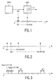
- Fig. 1 illustrates basic features of the invention.
- a frequency-synthesis circuit SYNTH generates a stepped-frequency signal Ssf whose frequency can be varied in steps.
- a synchronization circuit LOOP synchronizes a tuning oscillator LO with the stepped-frequency signal.
- Fig. 2 illustrates the following additional feature.
- the integer frequency-relationship between the stepped-frequency signal and the tuning oscillator is adjustable.
- the Fig. 2 feature takes the following aspects into consideration.
- the extent to which an oscillator can be tuned, on the one hand, and the spectral purity of the oscillator, on the other hand, are criteria which generally conflict with each other. If an oscillator needs to be tuned throughout a relatively wide frequency range, its frequency needs to change to a relatively large extent as a function of a frequency control signal. Consequently, the oscillator will be relatively sensitive to any disturbance in the frequency control signal, which disturbance may be noise or a signal leaking from another circuit.
- the frequency of the stepped-frequency signal needs to be varied throughout a smaller frequency range in order to tune the receiver throughout a desired band, than if the Fig. 2 feature is not applied. Consequently, any oscillator in the frequency-synthesizer circuit which provides the stepped-frequency signal needs to be tuned to a relatively small extent. This will be beneficial to the spectral purity of the stepped-frequency signal, on which the spectral purity of the tuning oscillator also depends, particularly if the synchronization circuit has a relatively large bandwidth. Thus, the Fig. 2 feature contributes to the tuning oscillator's spectral purity and, therefore, to the receiver's performance in terms of interference immunity.
- Fig. 3 illustrates the following additional feature.
- the size of the steps in which the frequency of the stepped-frequency signal can be varied, is adjustable.
- the Fig. 3 feature takes into consideration that the sizes of the steps in which the tuning-oscillator's frequency is varied, is equal to the sizes of the steps in which the stepped-frequency signal is varied, multiplied by the integer frequency-relationship between the tuning oscillator and the stepped-frequency signal. If the Fig. 2 feature is applied, the integer frequency-relationship will not be constant.
- the Fig. 3 feature allows compensation for this so as to achieve the desired uniform tuning step-size ⁇ F.
- the synchronization circuit has a bandwidth BWloop which covers at least a substantial portion of a typical baseband BB associated with a type of transmission signal which can be processed by the receiver.
- a transmission signal TS is usually formed by a carrier C which is modulated with information INF.
- the baseband BB is the frequency band occupied by the information INF which modulates the carrier C.
- an analog satellite television broadcast signal is a type of transmission signal which has a typical baseband of, say, 5 MHz.
- an FM-radio mono-broadcast signal is a type of transmission signal which has a typical baseband of, say, 15 kHz, whereas an FM-radio stereo-broadcast signal has a typical baseband of, say, 0 to 53 kHz.
- Fig. 4 visualizes the bandwidth BWloop of the synchronization circuit by means of a graph.
- the horizontal axis represents the frequency and the vertical axis indicates the extent to which the synchronization circuit reduces a synchronization error between the tuning oscillator and the stepped-frequency signal.
- the number 1 on the vertical axis means that the synchronization error is practically eliminated, the number 0 means that the synchronization error is not reduced.
- Synchronization errors which fall within the synchronization circuit's bandwidth BWloop are substantially eliminated, but synchronization errors which fall outside the synchronization circuits's bandwidth BWloop are not reduced or only to a relatively small extent.
- the tuning oscillator will provide an output signal which comprises a certain amount of noise centred around the oscillation frequency.
- a frequency conversion in which the tuning oscillator takes part will effectively impose this tuning-oscillator noise on the transmission signal to which the receiver is tuned. This will adversely affect the extent to which the receiver is capable of correctly recovering the information transmitted.
- the tuning-oscillator noise which is within a baseband distance from the oscillation frequency, plays an important role in this respect.
- the tuning-oscillator noise within a baseband distance from the oscillation frequency will be substantially determined by the noise in the stepped-frequency signal. This is because the synchronization circuit imposes. as it were, the noise in the stepped-frequency signal which is within its bandwidth BWloop, on the tuning oscillator. Consequently, if the tuning oscillator by itself is noisier than the stepped-frequency signal, the synchronization circuit will effectively perform a noise clean-up action within its bandwidth.
- the Fig. 4 feature allows use of a relatively noisy tuning oscillator without a significant deterioration of the receiver's performance in terms of correctly recovering the information transmitted. It should be noted that this also applies in the case of a non-integer frequency-relationship between the stepped-frequency signal and the tuning oscillator.
- the tuning oscillator may be wholly or partially realized in the form of an integrated circuit. Furthermore, it may also operate with a relatively low supply voltage and with a relatively small power consumption. All these factors contribute to reducing tuning-oscillator radiation which may cause interference problems. In particular, in a direct-conversion receiver, tuning-oscillator radiation needs to be relatively low so as to avoid problems of self-reception. Furthermore, if the tuning oscillator is wholly or partially included in an integrated circuit, it will be relatively easy to obtain mutually phase-shifted tuning-oscillator signals which are required in many types of receivers.
- the tuning oscillator may operate with a relatively low supply voltage, it will generally not need a supply voltage which is different from that with which other circuitry operates.
- the Fig. 4 feature may contribute to cost-efficiency, low power consumption, and/or overcoming realization problems in many type of receivers.
- Fig. 5 illustrates an example of a receiver in accordance with the invention which includes the Figs. 1-4 features described hereinbefore.
- the Fig. 5 receiver comprises an input circuit RFI, a mixer circuit MIX, and an intermediate frequency and demodulation circuit IFD.
- the mixer circuit MIX receives in-phase and quadrature mixing-signals Imix and Qmix from the tuning oscillator LO.
- the synthesizer circuit SYNTH and the synchronization circuit LOOP form, in combination, a tuning system which controls the frequency of the in-phase and quadrature mixing-signals Imix and Qmix in accordance with tuning command data TCD.
- the tuning command data TCD may be provided by a controller which is not shown in Fig. 5.
- the functions of the input circuit RFI, the mixer circuit MIX, and the intermediate frequency and demodulation circuit IFD will be clear to those skilled in the art. Therefore, these circuits are not further discussed hereinafter.
- a programmable divider DIV1 divides an output signal of the tuning oscillator LO by a factor of Nband. Accordingly, a frequency-divided tuning oscillator signal is obtained whose frequency is Flo ⁇ Nband.
- a phase/frequency detector PFD1 provides a synchronization error signal as a function of the synchronization error between the stepped-frequency signal Ssf and the frequency-divided tuning oscillator signal.
- the synchronization error signal is passed to the tuning oscillator LO via a loop filter LFP1 which has a relatively wide pass-band.
- the tuning oscillator LO is realized as an integrated RC-type oscillator which comprises a voltage-to-current converter V/I, a band-switching current source Iband and a current controlled oscillator circuit CCO.
- the band-switching current source Iband may be used to coarsely tune the tuning oscillator LO to a certain frequency band, or a portion thereof, on the basis of the tuning command data TCD.
- the frequency-synthesizer circuit SYNTH includes a voltage-controlled oscillator VCO which provides the stepped-frequency signal Ssf.
- a programmable divider DIV2 divides the frequency of the voltage-controlled oscillator's output signal by a factor of Ntune before it is supplied to a phase/frequency detector PFD2.
- the phase/frequency detector PFD also receives a signal providing an adjustable reference-frequency Fref which is obtained by carrying out two frequency divisions on a signal from a reference frequency source FXTAL.
- a programmable divider DIV3 carries out a first frequency division by the factor of Nband.
- a programmable divider DIV4 carries out a second frequency division by a factor of M.
- the phase/frequency detector provides, in response to the signals supplied thereto, a frequency control signal to the voltage-controlled oscillator VCO via a loop filter LPF2 which has a relatively narrow pass-band.
- the controller calculates the respective division factors Nband, Ntune and M for the programmable dividers DIV1/DIV3, DIV2 and DIV4.
- the division factor Nband is such that the frequency-divided tuning oscillator signal, whose frequency is Flo ⁇ Nband, falls within a frequency range through which the voltage-controlled oscillator VCO can be tuned. This frequency range may be relatively small if the division factor Nband is adjusted in accordance with the desired tuning-oscillator frequency Flo. In this way, a total frequency range through which the tuning oscillator LO should be tunable, can be effectively divided into different frequency subranges. Each frequency subrange is then associated with a division factor Nband. Since the division factor Nband is also used to divide the signal from the reference-frequency source FXTAL, a constant tuning step-size ⁇ F is achieved.
- the table below illustrates an application of the Fig. 5 receiver in the field of digital satellite TV-reception.
- Digital satellite TV-broadcasting takes place in a frequency range between, say, 950 MHz and 2150 MHz.
- the tuning oscillator LO is tuned throughout the frequency range between 950 MHz and 2150 MHz in 1 MHz steps.
- the 1 Mhz steps may be obtained, for example, if the reference-frequency source FXTAL provides a 4 Mhz signal and the division ratio M is 4.
- the rows of the table represent four frequency subranges SR1, SR2, SR3 and SR4 into which the frequency range between 950 MHz and 2150 MHz is effectively divided.
- the columns of the table list the following for each of the four frequency subranges SR1, SR2, SR3 and SR4: the frequency of the tuning oscillator Flo. the division factor Nband, the adjustable reference-frequency Fref, and the division factor Ntune, respectively.
- Flo (MHz) Nband Fref (kHz) Ntune SR1 950-1228 4 250 950-1228 SR2 1228-1535 5 200 1228-1535 SR3 1535-1840 6 166.67 1535-1840 SR4 1840-2150 7 142.85 1840-2150
- the voltage-controlled oscillator VCO only needs to be tuned throughout a relative small frequency range between 237 MHz and 307 MHz.
- Fig. 6 illustrates the noise behavior of the tuning oscillator LO in the above-described application of the Fig. 5 receiver.
- Fig. 6 is a graph of noise power spectral density Pn versus a distance in frequency dF with respect to the oscillation frequency.
- the noise power spectral density Pn is expressed in decibels with respect to the carrier power per Hertz (dBc/Hz).
- Fig. 6 shows two plots P1 and P2 which represent, respectively, the noise behavior of the tuning oscillator LO by itself, and the noise behavior when it forms part of the Fig. 5 receiver.
- Fig. 6 visualizes the noise clean-up action which the synchronization circuit LOOP carries out below a frequency FX.
- the frequency FX approximately corresponds to the bandwidth BWloop of the synchronization circuit LOOP.
- the Fig. 5 receiver includes some additional features which have not been highlighted hereinbefore.
- the use of phase/frequency detectors contributes to a reliable and relatively fast operation of the Fig. 5 receiver.
- the use of phase/frequency detectors is also advantageous in terms of spectral purity, because phase/frequency detectors produce relatively few spurious products.
- European patent application 96202486.5 (attorney's docket PHN 15.978), which is herein incorporated by reference, describes suitable phase/frequency detectors.
- Another additional feature, which is included in the Fig. 5 receiver, is that the phase/frequency detectors have programmable characteristics. That is, the magnitude of the output signal for a certain synchronization error is adjustable.
- a change in the frequency division factors of programmable dividers DIV1 and DIV2 may be compensated for so as to keep the bandwidth BWloop of the synchronization circuit LOOP, and that of the synthesizer circuit SYNTH, substantially constant. This may be important, because in many applications the bandwidth is a delicate compromise between various performance aspects.
Landscapes
- Engineering & Computer Science (AREA)
- Computer Hardware Design (AREA)
- Microelectronics & Electronic Packaging (AREA)
- Superheterodyne Receivers (AREA)
- Stabilization Of Oscillater, Synchronisation, Frequency Synthesizers (AREA)
Claims (10)
- Abstimmsystem, das die nachfolgenden Elemente umfasst:dadurch gekennzeichnet, dass der erste Teiler (DIV3) mit der Bezugsfrequenzquelle (FXAL) zum Teilen der Bezugsfrequenz (Fxtal) durch einen ganzzahligen Faktor (Nband) gekoppelt ist und das der zweite Teiler (DIV1) mit dem Abstimmoszillator (LO) gekoppelt ist zum Teilen der Abstimmoszillatorfrequenz (Flo) durch einen ganzzahligen Faktor (Nband) zum Liefern eines ganzzahligen Frequenzverhältnisses (Flo = Nband.Fsf) zwischen der Frequenz (Fsf) des gestuften Frequenzsignals (Ssf) und der Abstimmoszillatorfrequenz (Flo).eine Frequenz-Syntheseschleife (SYNTH) zum Erzeugen eines gestuften Frequenzsignals (Ssf) mit einer Frequenz (Fsf), die stufenweise variiert werden kann, wobei die Frequenz-Syntheseschleife (SYNTH) eine Bezugsfrequenzquelle (FXTAL) mit einer Bezugs frequenz (Fxtal), sowie einen ersten Teiler (DIV3) aufweist; undeine Synchronisationsschaltung (LOOP) zum Synchronisieren eines Abstimmoszillators (LO) mit einer Abstimmoszillatorfrequenz (Flo) mit dem gestuften Frequenzsignal (Ssf), wobei die Synchronisationsschaltung (loop) einen zweiten Teiler (DIV1) aufweist,
- Abstimmsystem nach Anspruch 1, dadurch gekennzeichnet, dass die Frequenz-Syntheseschleife (SYNTH) einen dritten Teiler (DIV2) aufweist zum Teilen der Frequenz (Fsf) des gestuften Frequenzsignals (Ssf) durch einen anderen Faktor (Ntune), wobei die Schleife vorgesehen ist zum Schaffen einer Beziehung zwischen der Bezugsfrequenz (Fxtal) und der Frequenz (Fsf), und zwar:
- Abstimmsystem nach Anspruch 2, dadurch gekennzeichnet, dass ein Gebiet von Abstimmoszillatorfrequenzen (Flo) dadurch selektierbar ist, dass Kombinationen des Faktors (Nband) und des anderen Faktors (Ntune) selektiert werden, wobei die Kombinationen zu einem Gebiet von Frequenzen (Fsf) führen, das verhältnismäßig ein kleineres Gebiet ist als das Gebiet der Abstimmoszillatorfrequenzen (Flo).
- Abstimmsystem nach Anspruch 1, dadurch gekennzeichnet, dass die Synchronisationsschaltung (LOOP) einen Phasen/Frequenzdetektor (PFD1) aufweist zum Schaffen eines Frequenzsteuersignals für den Abstimmoszillator (LO) als eine Funktion eines Synchronisationsfehlers zwischen dem gestuften Frequenzsignal (Ssf) und dem Abstimmoszillator (LO).
- Abstimmsystem nach Anspruch 4, dadurch gekennzeichnet, dass die Beziehung zwischen dem Frequenzsteuersignal und dem Synchronisationsfehler einstellbar ist.
- Abstimmsystem nach Anspruch 5, dadurch gekennzeichnet, dass die Beziehung in Abhängigkeit von dem Faktor (Nband) einstellbar ist, und zwar zum Reduzieren der Bandbreitenvariationen der Synchronisationsschaltung (LOOP).
- Abstimmsystem nach Anspruch 1, dadurch gekennzeichnet, dass die Frequenz-Syntheseschleife (SYNTH) einen spannungsgeregelten Oszillator (CO) aufweist zum Schaffen des gestuften Frequenzsignals (Ssf) und einen Frequenzdetektor (PFD2) zum Schaffen eines Frequenzregelsignals für den spannungsgeregelten Oszillator (VCO) als eine Funktion eines Synchronisationsfehlers zwischen dem gestuften Frequenzsignal (Ssf) und dem Bezugsoszillators (FXTAL).
- Empfänger mit einem Abstimmsystem nach Anspruch 1, weiterhin mit einer Mischstufe, die mit dem Abstimmoszillator gekoppelt ist.
- Empfänger nach Anspruch 8, dadurch gekennzeichnet, dass die Synchronisationsschaltung (LOOP) eine Bandbreite (BWloop) hat, die wenigstens einen wesentlichen Teil eines typischen Basisbandes (BB) bedeckt, das mit einem Typ eines Übertragungssignals (TS) assoziiert ist, das durch den Empfänger verarbeitet werden kann.
- Abstimmverfahren, wobei dieses Verfahren die nachfolgenden Verfahrensschritte umfasst:das Erzeugen eines gestuften Frequenzsignals (Ssf) mit einer Frequenz (Fsf), die stufenweise variiert werden kann; unddas Synchronisieren eines Abstimmoszillators (LO) mit einer Abstimmoszillatorfrequenz (Flo) mit einem gestuften Frequenzsignal (Ssf), dadurch gekennzeichnet, dass der Verfahrensschritt der Erzeugung Folgendes umfasst:das Teilen einer Bezugsfrequenz durch einen ganzzahligen Faktor (Nband); und dass der Verfahrensschritt der Synchronisation Folgendes umfasst:das Teilen der Abstimmoszillatorfrequenz (Flo) durch den ganzzahligen Faktor (Nband) zum Schaffen eines ganzzahligen Frequenzverhältnisses (Flo = Nband.Fsf) zwischen der Frequenz (Fsf) des gestuften Frequenzsignals (Ssf) und der Abstimmoszillatorfrequenz (Flo).
Priority Applications (1)
| Application Number | Priority Date | Filing Date | Title |
|---|---|---|---|
| EP98903240A EP0932935B1 (de) | 1997-03-18 | 1998-02-27 | Abstimmsystem für empfänger |
Applications Claiming Priority (4)
| Application Number | Priority Date | Filing Date | Title |
|---|---|---|---|
| EP97200821 | 1997-03-18 | ||
| EP97200821 | 1997-03-18 | ||
| EP98903240A EP0932935B1 (de) | 1997-03-18 | 1998-02-27 | Abstimmsystem für empfänger |
| PCT/IB1998/000255 WO1998042076A2 (en) | 1997-03-18 | 1998-02-27 | Receiver tuning system |
Publications (2)
| Publication Number | Publication Date |
|---|---|
| EP0932935A1 EP0932935A1 (de) | 1999-08-04 |
| EP0932935B1 true EP0932935B1 (de) | 2004-01-07 |
Family
ID=26146266
Family Applications (1)
| Application Number | Title | Priority Date | Filing Date |
|---|---|---|---|
| EP98903240A Expired - Lifetime EP0932935B1 (de) | 1997-03-18 | 1998-02-27 | Abstimmsystem für empfänger |
Country Status (3)
| Country | Link |
|---|---|
| EP (1) | EP0932935B1 (de) |
| JP (1) | JP2000511031A (de) |
| DE (1) | DE69820978T2 (de) |
-
1998
- 1998-02-27 DE DE69820978T patent/DE69820978T2/de not_active Expired - Fee Related
- 1998-02-27 EP EP98903240A patent/EP0932935B1/de not_active Expired - Lifetime
- 1998-02-27 JP JP10529285A patent/JP2000511031A/ja not_active Abandoned
Also Published As
| Publication number | Publication date |
|---|---|
| DE69820978D1 (de) | 2004-02-12 |
| JP2000511031A (ja) | 2000-08-22 |
| EP0932935A1 (de) | 1999-08-04 |
| DE69820978T2 (de) | 2004-12-09 |
Similar Documents
| Publication | Publication Date | Title |
|---|---|---|
| US6665523B1 (en) | Receiver tuning system | |
| AU680481B2 (en) | Frequency synthesizer | |
| US6094236A (en) | Tuner circuit | |
| US8013681B2 (en) | Wide spectrum radio transmit architecture | |
| CA2010176C (en) | Tuner station selecting apparatus | |
| US4521916A (en) | Frequency synthesis tuning control system for a double-conversion tuner | |
| KR19990071777A (ko) | 피드포워드를 갖는 고안정성 주파수 합성기 루프 | |
| US5790942A (en) | Frequency modulation radio transmission device | |
| JPH11501471A (ja) | 単一の局部発振器を有する広い周波数範囲のテレビジョン・チューナ | |
| US6895063B1 (en) | Frequency changer and digital tuner | |
| US6091943A (en) | Combining oscillator with a phase-indexed control circuit for a radio receiver | |
| US4245351A (en) | AFT Arrangement for a phase locked loop tuning system | |
| EP0932935B1 (de) | Abstimmsystem für empfänger | |
| GB2250877A (en) | Shifting spurious frequencies away from signal frequency | |
| KR101757445B1 (ko) | 주파수 합성 장치 및 이의 주파수 합성 방법 | |
| US6433830B1 (en) | Off-air phase lock technique | |
| WO1998042076A2 (en) | Receiver tuning system | |
| US4095190A (en) | Tuning system | |
| EP1689083B1 (de) | Am/fm-funkempfänger und darin verwendete empfangsoszillatorschaltung | |
| US5221911A (en) | Receiver having pll frequency synthesizer with rc loop filter | |
| US20050089119A1 (en) | Receiver | |
| US20020024393A1 (en) | Electronic circuit for and a method of controlling the output frequency of a frequency synthesizer | |
| EP1091487B1 (de) | Methode und Vorrichtung zur Unterdrückung von zur Selbst-Stummschaltung führenden Signalen in Synthesizer-Empfängern | |
| KR100442432B1 (ko) | 디지털 티브이 중계기의 주파수 변환장치 | |
| GB2373113A (en) | Improvements in or relating to fast frequency-hopping synthesisers |
Legal Events
| Date | Code | Title | Description |
|---|---|---|---|
| PUAI | Public reference made under article 153(3) epc to a published international application that has entered the european phase |
Free format text: ORIGINAL CODE: 0009012 |
|
| 17P | Request for examination filed |
Effective date: 19981218 |
|
| AK | Designated contracting states |
Kind code of ref document: A1 Designated state(s): DE FR GB |
|
| 17Q | First examination report despatched |
Effective date: 20021113 |
|
| GRAH | Despatch of communication of intention to grant a patent |
Free format text: ORIGINAL CODE: EPIDOS IGRA |
|
| GRAA | (expected) grant |
Free format text: ORIGINAL CODE: 0009210 |
|
| GRAS | Grant fee paid |
Free format text: ORIGINAL CODE: EPIDOSNIGR3 |
|
| AK | Designated contracting states |
Kind code of ref document: B1 Designated state(s): DE FR GB |
|
| REG | Reference to a national code |
Ref country code: GB Ref legal event code: FG4D |
|
| REG | Reference to a national code |
Ref country code: GB Ref legal event code: 746 Effective date: 20040109 |
|
| REF | Corresponds to: |
Ref document number: 69820978 Country of ref document: DE Date of ref document: 20040212 Kind code of ref document: P |
|
| ET | Fr: translation filed | ||
| PLBE | No opposition filed within time limit |
Free format text: ORIGINAL CODE: 0009261 |
|
| STAA | Information on the status of an ep patent application or granted ep patent |
Free format text: STATUS: NO OPPOSITION FILED WITHIN TIME LIMIT |
|
| REG | Reference to a national code |
Ref country code: FR Ref legal event code: D6 |
|
| 26N | No opposition filed |
Effective date: 20041008 |
|
| PGFP | Annual fee paid to national office [announced via postgrant information from national office to epo] |
Ref country code: GB Payment date: 20070223 Year of fee payment: 10 |
|
| PGFP | Annual fee paid to national office [announced via postgrant information from national office to epo] |
Ref country code: DE Payment date: 20070410 Year of fee payment: 10 |
|
| PGFP | Annual fee paid to national office [announced via postgrant information from national office to epo] |
Ref country code: FR Payment date: 20070226 Year of fee payment: 10 |
|
| GBPC | Gb: european patent ceased through non-payment of renewal fee |
Effective date: 20080227 |
|
| REG | Reference to a national code |
Ref country code: FR Ref legal event code: ST Effective date: 20081031 |
|
| PG25 | Lapsed in a contracting state [announced via postgrant information from national office to epo] |
Ref country code: DE Free format text: LAPSE BECAUSE OF NON-PAYMENT OF DUE FEES Effective date: 20080902 |
|
| PG25 | Lapsed in a contracting state [announced via postgrant information from national office to epo] |
Ref country code: FR Free format text: LAPSE BECAUSE OF NON-PAYMENT OF DUE FEES Effective date: 20080229 |
|
| PG25 | Lapsed in a contracting state [announced via postgrant information from national office to epo] |
Ref country code: GB Free format text: LAPSE BECAUSE OF NON-PAYMENT OF DUE FEES Effective date: 20080227 |