EP0933687A1 - Belichtungssteuerung für einen Rasterausgabeabtaster in einem elektrophotographischen Mehrfarbendrucker - Google Patents
Belichtungssteuerung für einen Rasterausgabeabtaster in einem elektrophotographischen Mehrfarbendrucker Download PDFInfo
- Publication number
- EP0933687A1 EP0933687A1 EP99100212A EP99100212A EP0933687A1 EP 0933687 A1 EP0933687 A1 EP 0933687A1 EP 99100212 A EP99100212 A EP 99100212A EP 99100212 A EP99100212 A EP 99100212A EP 0933687 A1 EP0933687 A1 EP 0933687A1
- Authority
- EP
- European Patent Office
- Prior art keywords
- light
- light source
- image
- photoreceptor
- photosensitive member
- Prior art date
- Legal status (The legal status is an assumption and is not a legal conclusion. Google has not performed a legal analysis and makes no representation as to the accuracy of the status listed.)
- Granted
Links
- 239000000463 material Substances 0.000 claims description 10
- 108091008695 photoreceptors Proteins 0.000 abstract description 64
- 238000007599 discharging Methods 0.000 abstract description 7
- 238000011161 development Methods 0.000 description 13
- 238000013461 design Methods 0.000 description 4
- 230000003287 optical effect Effects 0.000 description 4
- 239000003086 colorant Substances 0.000 description 3
- 238000000034 method Methods 0.000 description 3
- 238000012546 transfer Methods 0.000 description 3
- 230000008859 change Effects 0.000 description 2
- 230000000694 effects Effects 0.000 description 2
- 238000002955 isolation Methods 0.000 description 2
- 230000004044 response Effects 0.000 description 2
- 230000009471 action Effects 0.000 description 1
- 230000005540 biological transmission Effects 0.000 description 1
- 230000001419 dependent effect Effects 0.000 description 1
- 238000010586 diagram Methods 0.000 description 1
- 230000004907 flux Effects 0.000 description 1
- 238000003384 imaging method Methods 0.000 description 1
- 239000007788 liquid Substances 0.000 description 1
- 230000007246 mechanism Effects 0.000 description 1
- 238000012986 modification Methods 0.000 description 1
- 230000004048 modification Effects 0.000 description 1
- 230000000737 periodic effect Effects 0.000 description 1
- 230000008569 process Effects 0.000 description 1
- 238000002310 reflectometry Methods 0.000 description 1
- 238000009877 rendering Methods 0.000 description 1
Images


Classifications
-
- G—PHYSICS
- G03—PHOTOGRAPHY; CINEMATOGRAPHY; ANALOGOUS TECHNIQUES USING WAVES OTHER THAN OPTICAL WAVES; ELECTROGRAPHY; HOLOGRAPHY
- G03G—ELECTROGRAPHY; ELECTROPHOTOGRAPHY; MAGNETOGRAPHY
- G03G15/00—Apparatus for electrographic processes using a charge pattern
- G03G15/01—Apparatus for electrographic processes using a charge pattern for producing multicoloured copies
- G03G15/0105—Details of unit
- G03G15/011—Details of unit for exposing
-
- H—ELECTRICITY
- H04—ELECTRIC COMMUNICATION TECHNIQUE
- H04N—PICTORIAL COMMUNICATION, e.g. TELEVISION
- H04N1/00—Scanning, transmission or reproduction of documents or the like, e.g. facsimile transmission; Details thereof
- H04N1/46—Colour picture communication systems
- H04N1/50—Picture reproducers
- H04N1/506—Reproducing the colour component signals picture-sequentially, e.g. with reproducing heads spaced apart from one another in the subscanning direction
-
- G—PHYSICS
- G03—PHOTOGRAPHY; CINEMATOGRAPHY; ANALOGOUS TECHNIQUES USING WAVES OTHER THAN OPTICAL WAVES; ELECTROGRAPHY; HOLOGRAPHY
- G03G—ELECTROGRAPHY; ELECTROPHOTOGRAPHY; MAGNETOGRAPHY
- G03G2215/00—Apparatus for electrophotographic processes
- G03G2215/01—Apparatus for electrophotographic processes for producing multicoloured copies
- G03G2215/0167—Apparatus for electrophotographic processes for producing multicoloured copies single electrographic recording member
- G03G2215/0174—Apparatus for electrophotographic processes for producing multicoloured copies single electrographic recording member plural rotations of recording member to produce multicoloured copy
Definitions
- the present invention relates to laser exposure control for use in a raster output scanner (ROS) for creating electrostatic latent images from electronic data.
- ROS raster output scanner
- Electrophotographic "laser” printers wherein a modulating, scanning laser is projected onto a photoconductive surface to create an image to be printed, are well known.
- a raster output scanner ROS
- the ROS provides a laser beam which switches on and off according to electronic image data associated with the desired image to be printed, exposing the charged photoreceptor point by point as the beam moves, or scans, across its surface.
- the surface of the photoreceptor is selectively imagewise discharged by the laser beam in locations to be printed white, to form the desired image on the photoreceptor.
- a common technique for deflecting the modulated laser beam to form a scan line across the photoreceptor surface uses a motor-driven rotating optical polygon with multiple reflecting surfaces; the laser beam from the laser source is reflected by the facets of the polygon, creating a scanning motion of the beam, forming a sharply focused scan line across the photoreceptor surface.
- a closely spaced regular array of scan lines on a photoreceptor collectively forms a raster of the desired latent image.
- the discharging effect of a laser should be uniform whether or not the laser is passing through one or more layers of toner, which in turn means that the intensity of a laser should be increased in areas where the laser must pass through one or more layers of toner.
- Previously-placed toner will interfere with the transmission of light from the laser to the charged surface of the photoreceptor. Exactly where, within an image to be printed, one or more layers of previously-placed toner will be for a particular portion of a scanline is ultimately dependent on the exact nature of the image being created, and will of course change depending on what specific portion of the image is being printed. There therefore exists a need to monitor and adjust the intensity of a laser discharging any particular portion of a photoreceptor in an IOI color printing apparatus.
- US-A-4,314,283 and US-A-4,321,630 each disclose a type of elongated light collector suitable for use in measuring the instantaneous intensity of a moving laser beam spot.
- US-A-5,497,181 discloses a system for controlling individual spot exposure in a laser printer, wherein the real-time light output of a laser is associated with an integrator which directly controls the pulse width, or exposure duration, of the laser on individual pixel areas in an image being printed.
- an apparatus for creating an image on a photosensitive surface There is provided a light source, and means for causing the light source to expose a plurality of image areas forming a scanline on the photosensitive surface.
- a light collector extending parallel to the scanline, is disposed to collect light from the light source reflected from the photosensitive surface and cause output of a signal related to the intensity of the reflected light.
- Means are provided for controlling the exposure of light from the light source on an image area, based on the signal.
- an apparatus for creating an image on a surface of a photosensitive member There is provided a light source, and means for causing the light source to expose a plurality of image areas on the photosensitive surface.
- a light collector is disposed to collect light from the light source transmitted through the photosensitive member and cause an output of a signal related to the intensity of the transmitted light.
- an electrophotographic printing apparatus comprising a photosensitive member having a surface, a light source, and means for causing the light source to expose a plurality of image areas on the surface of the photosensitive member.
- Means are provided for placing marking material of a first type on the surface of the photosensitive member.
- a light collector is disposed to collect light from the light source which interacts with the photosensitive member, and outputs a signal related to the intensity of the interacting light.
- Means are provided for controlling the exposure of light from the light source on an image area, based on the signal.
- an electrophotographic printing apparatus comprising: a photosensitive member having a surface; at least one light source; means for causing a light source to expose a plurality of image areas forming a first image scanline on the surface of the photosensitive member; means for placing marking material of a first type on the surface of the photosensitive member, thereby developing a first image on the photosensitive member; a light collector disposed to collect light from the light source interacting with the photosensitive member at an image area being exposed by the light source, and output a signal related to intensity of the interacting light, thereby determining whether marking material of the first type was placed on said image area; means for causing a light source to expose a plurality of image areas forming a second image scanline on the surface of the photosensitive member; and means for controlling the exposure of light from a light source on an image area when exposing the second image scanline, based on whether marking material of the first type was placed on said image area.
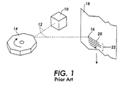
- FIG. 1 shows the basic configuration of a scanning system used, for example, in an electrophotographic printer or facsimile machine.
- a laser source 10 which may include a He-Ne laser, or laser diode, produces a collimated laser beam, also referred to as a "writing beam," 12 which is reflected by the facets of a rotating polygon 14. Each facet of the polygon 14 in turn deflects the writing beam 12 to create an illuminated spot 16 on the pre-charged surface of photoreceptor 18, which in this case is a moving belt.
- Laser source 10 also includes means for modulating the beam 12 according to image data entered therein.
- writing beam 12 is momentarily interrupted through the action of the modulator within source 10, so that the pixel at that location on the surface of photoreceptor 18 will not be discharged.
- digital data input into laser source 10 is rendered line by line as an electrostatic latent image on the surface of photoreceptor 18.
- the rotational motion of polygon 14 results in a spot 16 moving across the surface of photoreceptor 18 to form a scan line 20 of selectively discharged pixel-sized areas on photoreceptor 18.
- the surface of photoreceptor 18 is slowly translated at a constant velocity so that the periodic scanning of spot 16 across the moving photoreceptor 18 creates an evenly spaced closely spaced array of scan lines 20, called a raster 22, on the surface of photoreceptor 18, forming the desired continuous image to be printed.
- a raster 22 on the surface of photoreceptor 18, forming the desired continuous image to be printed.
- FIG 2 is a simplified elevational view of the basic architecture for an image-on-image (IOI) type electrophotographic printer.
- a laser source 10 reflects a laser beam 12 off the facets of a rotating polygon 14 to create an electrostatic latent image on a photoreceptor 18.
- photoreceptor 18 rotates about a series of rollers so that a particular area of the surface of photoreceptor 18 can be recycled numerous times past the beam 12.
- a charge corotron 30, which places a uniform charge on the main surface of photoreceptor 18 so that it may be imagewise discharged by laser beam 12; a plurality of development units, here indicated as 32 and 34; and a transfer corotron 36.
- the latent image created by the scanning of beam 12 is developed with one or the other development units 32 or 34, and then eventually the toner associated with the developed image is transferred at transfer corotron 36 to a sheet, such as a sheet of paper, which in turn is fused by a fuser generally indicated as 38.
- development units 32 and 34 there are at least two development units 32 and 34 arranged along the length of photoreceptor 18, and one or the other development unit can be selectably activated to place a particular type of toner (or other marking material, such as liquid ink) in the suitably charged or discharged areas created by beam 12.
- toner or other marking material, such as liquid ink
- the area of photoreceptor 18 is cycled numerous times past charge corotron 30, beam 12, and the development units 32, 34.
- the area of photoreceptor 18 is charged by corotron 30 and imagewise discharged by beam 12 in areas corresponding to those intended to have color C1 thereon. After imagewise discharge by beam 12, this area is moved past the activated development unit 32, which places toner of color C1 in the suitably charged or discharged areas.
- the area of photoreceptor 18 is once again charged by charge corotron 30, and then discharged by beam 12 in areas corresponding to those desired to include color C2 therein. After discharging by beam 12, the area moves past development unit 32, which in this cycle is inactivated, and then to development unit 34 which is activated to convey toner of color C2 to the suitably charged or discharged areas on photoreceptor 18.
- the photoreceptor belt 18 Only after all of the desired colors are placed on the area of the photoreceptor desired to have the multicolor or full-color image is the complete set of toner layers (such as including toner of color C1 and color C2) transferred in one step with transfer corotron 36 onto a sheet.
- the photoreceptor belt 18 In a four-color system, the photoreceptor belt 18 must circulate four times, receiving a color each time, before the complete image is transferred in one step.
- the exposure of the laser should be increased where the laser must pass through one or more layers of toner.
- This increase in exposure can occur either by momentarily increasing the laser intensity, increasing the time duration of laser exposure for a particular pixel-sized area, or a combination of both techniques.
- Figures 3 and 4 are, respectively, elevational views of a basic architecture for an apparatus for exposure control of a laser beam 12 from source 10 which is used to discharge a series of small areas on the surface of photoreceptor 18. In both cases, the surface of photoreceptor 18 has placed thereon, at unpredictable locations, areas of previously-placed toner indicated as T. The discharging behavior of the beam 12 will vary whether or not the beam 12 must pass through one or more toner layers T or not.
- the present invention provides what is here called a "light collector” 40, which sends a signal representative of the light received thereon to a control system generally indicated as 50.
- Light collector 40 is an optical element of a design known in the art which conducts light received thereon to a desired location, in this case a photodetector which will be described in detail below.
- the control system 50 in turn controls the behavior of laser source 10 to control the real-time exposure of beam 12 on a small area of photoreceptor 18. Once again, this control may involve controlling either the power associated with beam 12, the pulse duration of beam 12, or both.
- light collector 40 is placed in a position whereby a portion of beam 12 reflected against the surface of photoreceptor 18, indicated as 12a, is accepted by light collector 40.
- photoreceptor 18 moves a small distance causing beam 12 to reflect not off the bare photoreceptor 18 but rather a toner layer T, that the amount of light being reflected to light collector 40 will be significantly changed, because the toner will have a different reflectivity than the bare surface of the photoreceptor.
- the signal output associated with light collector 40 will affect the control system 50, which will in turn alter the exposure (typically, the power level and/or the pulse duration) associated with light source 10 while the beam 12 is still generally directed to the pixel area in question.
- Figure 4 shows an alternate arrangement of elements according to the present invention, wherein the light collector 40 is effectively disposed behind photoreceptor 18 but within the path of beam 12, so that a certain amount of light from beam 12, here indicated as 12b, will be transmitted through the translucent photoreceptor 18 and hit light collector 40.
- the light collector 40 will ultimately affect control system 50 to cause light source 10 to compensate for the light blockage caused by toner layer T.
- FIG 5 is a perspective view showing, in isolation, a light collector 40 associated with a photodetector generally indicated as 42.
- the light collector 40 which is a small-diameter, elongated optical element, is meant to extend across the width of photoreceptor 18 in a position which is parallel to the direction of, for example, a scanline 20 as shown in Figure 1 above. In this way, regardless of the specific position of the laser beam 12 at a particular time, a quantity of light either reflected from photoreceptor 18 or passing through photoreceptor 18 will hit the side of light collector 40 and be transferred to the relatively small photodetector 42 disposed at the end thereof.
- control system 50 can be any system which allows for compensation of the measured intensity of beam 12, either by increasing the power thereof or increasing the pulse duration while the beam 12 is exposing a particular pixel area.
- One disclosure which discloses a practical system for effecting such exposure control is US patent 5,497,181 assigned to the assignee hereof.
- the '181 disclosure discloses a photodetector disposed in the path of beam 12 between the source and the photoreceptor, the principle can be applied to the arrangement of a photodetector such as light collector 40 in the present invention.
- the disclosed embodiment of the invention is directed to an apparatus which uses a laser and rotating polygonal mirror to expose a series of pixel-sized image areas on the photoreceptor, it is conceivable that the claimed invention could be applied to an apparatus having a different type of light source, such as an LED bar.
Landscapes
- Physics & Mathematics (AREA)
- General Physics & Mathematics (AREA)
- Engineering & Computer Science (AREA)
- Multimedia (AREA)
- Signal Processing (AREA)
- Exposure Or Original Feeding In Electrophotography (AREA)
- Laser Beam Printer (AREA)
- Color Electrophotography (AREA)
Applications Claiming Priority (2)
| Application Number | Priority Date | Filing Date | Title |
|---|---|---|---|
| US4537 | 1998-01-08 | ||
| US09/004,537 US6011576A (en) | 1998-01-08 | 1998-01-08 | Exposure control for a raster output scanner in a multicolor electrophotographic printer |
Publications (2)
| Publication Number | Publication Date |
|---|---|
| EP0933687A1 true EP0933687A1 (de) | 1999-08-04 |
| EP0933687B1 EP0933687B1 (de) | 2001-09-26 |
Family
ID=21711273
Family Applications (1)
| Application Number | Title | Priority Date | Filing Date |
|---|---|---|---|
| EP99100212A Expired - Lifetime EP0933687B1 (de) | 1998-01-08 | 1999-01-07 | Belichtungssteuerung für einen Rasterausgabeabtaster in einem elektrophotographischen Mehrfarbendrucker |
Country Status (4)
| Country | Link |
|---|---|
| US (1) | US6011576A (de) |
| EP (1) | EP0933687B1 (de) |
| JP (1) | JPH11277803A (de) |
| DE (1) | DE69900304T2 (de) |
Citations (3)
| Publication number | Priority date | Publication date | Assignee | Title |
|---|---|---|---|---|
| US5497181A (en) * | 1992-06-29 | 1996-03-05 | Xerox Corporation | Dynamic control of individual spot exposure in an optical output device |
| US5654951A (en) * | 1996-05-20 | 1997-08-05 | Xerox Corporation | Dynamic switching speed control |
| US5751437A (en) * | 1997-01-21 | 1998-05-12 | Xerox Corporation | Development combination exposure and recharge scheme to eliminate development defects in two pass process color xerocolography |
Family Cites Families (16)
| Publication number | Priority date | Publication date | Assignee | Title |
|---|---|---|---|---|
| US4265532A (en) * | 1979-06-21 | 1981-05-05 | Logetronics Inc. | Photo printing by intensity and velocity modulation |
| US4321630A (en) * | 1980-09-02 | 1982-03-23 | Xerox Corporation | Linear integrating cavity light collector |
| US4314283A (en) * | 1980-09-02 | 1982-02-02 | Xerox Corporation | Diffraction based light collector |
| US4355882A (en) * | 1981-02-26 | 1982-10-26 | Xerox Corporation | Multiple function reproduction apparatus |
| US4685097A (en) * | 1985-07-25 | 1987-08-04 | Laser Magnetic Storage International Company | Power control system for a semiconductor laser |
| NL8701986A (nl) * | 1987-08-25 | 1989-03-16 | Oce Nederland Bv | Besturingsschakeling voor een laserprinter. |
| JP2675827B2 (ja) * | 1988-08-26 | 1997-11-12 | 富士通株式会社 | レーザ走査装置 |
| EP0649247B1 (de) * | 1988-09-06 | 2002-12-11 | Canon Kabushiki Kaisha | Belichtungsstärkesteuergerät |
| JP2771822B2 (ja) * | 1988-10-21 | 1998-07-02 | 株式会社リコー | 光照射画像形成装置 |
| US4998118A (en) * | 1989-07-03 | 1991-03-05 | Eastman Kodak Company | LED printhead with post lens optical feedback and method of controlling same |
| US5341165A (en) * | 1991-01-16 | 1994-08-23 | Canon Kabushiki Kaisha | Scanning controller for color electrophotographic apparatus |
| JP3445809B2 (ja) * | 1992-09-25 | 2003-09-08 | 株式会社東芝 | 画像形成装置及びその制御方法 |
| US5325383A (en) * | 1993-05-17 | 1994-06-28 | Eastman Kodak Company | Laser diode operated in hybrid modulation modes |
| US5552863A (en) * | 1995-02-21 | 1996-09-03 | Xerox Corporation | Xerographic printer wherein exposure and development are performed on opposite sides of the photoreceptor |
| US5600126A (en) * | 1995-06-20 | 1997-02-04 | Xerox Corporation | Method and apparatus for controlling the power output of multiple laser diodes |
| US5574527A (en) * | 1995-09-25 | 1996-11-12 | Xerox Corporation | Multiple use of a sensor in a printing machine |
-
1998
- 1998-01-08 US US09/004,537 patent/US6011576A/en not_active Expired - Lifetime
-
1999
- 1999-01-05 JP JP11000474A patent/JPH11277803A/ja not_active Withdrawn
- 1999-01-07 EP EP99100212A patent/EP0933687B1/de not_active Expired - Lifetime
- 1999-01-07 DE DE69900304T patent/DE69900304T2/de not_active Expired - Fee Related
Patent Citations (3)
| Publication number | Priority date | Publication date | Assignee | Title |
|---|---|---|---|---|
| US5497181A (en) * | 1992-06-29 | 1996-03-05 | Xerox Corporation | Dynamic control of individual spot exposure in an optical output device |
| US5654951A (en) * | 1996-05-20 | 1997-08-05 | Xerox Corporation | Dynamic switching speed control |
| US5751437A (en) * | 1997-01-21 | 1998-05-12 | Xerox Corporation | Development combination exposure and recharge scheme to eliminate development defects in two pass process color xerocolography |
Also Published As
| Publication number | Publication date |
|---|---|
| JPH11277803A (ja) | 1999-10-12 |
| DE69900304T2 (de) | 2002-04-25 |
| US6011576A (en) | 2000-01-04 |
| EP0933687B1 (de) | 2001-09-26 |
| DE69900304D1 (de) | 2001-10-31 |
Similar Documents
| Publication | Publication Date | Title |
|---|---|---|
| JP3295281B2 (ja) | レーザー走査光学装置 | |
| US6259879B1 (en) | Image forming apparatus which forms an inconspicuous dot pattern prior to image transfer | |
| US6108501A (en) | Color image forming apparatus and method | |
| GB2272867A (en) | Color image forming apparatus | |
| US5438354A (en) | Start-of-scan and end-of-scan optical element for a raster output scanner in an electrophotographic printer | |
| US20020085081A1 (en) | Image forming apparatus for maintaining a constant beam scanning state | |
| US6336019B2 (en) | Surface position and velocity measurement for photoreceptor belt | |
| US5300962A (en) | Compound optics for a raster output scanner in an electrophotographic printer | |
| US5774156A (en) | Image self-registration for color printers | |
| AU643304B2 (en) | Electronic single pass, two color printing system | |
| US6014154A (en) | Image self-registration for color printer | |
| EP0933923B1 (de) | Abbildungsvorrichtung und -verfahren | |
| US5285221A (en) | Color image electrophotographic apparatus having photosensitive body and intermediate transfer body | |
| US5257048A (en) | Optical element and photoreceptor registration system for a raster output scanner in an electrophotographic printer | |
| EP0933687B1 (de) | Belichtungssteuerung für einen Rasterausgabeabtaster in einem elektrophotographischen Mehrfarbendrucker | |
| US5716744A (en) | Dual beam color electrophotographic apparatus | |
| JP2000318211A (ja) | 画像形成装置 | |
| JP3057181B2 (ja) | 画像形成装置 | |
| JP3182619B2 (ja) | カラー画像形成装置 | |
| JPH10181091A (ja) | 画像形成装置 | |
| JPH05119571A (ja) | カラー画像形成装置 | |
| JP2596395B2 (ja) | カラー電子写真装置 | |
| US20250224689A1 (en) | Image forming apparatus | |
| JPH05119572A (ja) | カラー画像形成装置 | |
| JP3023722B2 (ja) | カラー画像形成装置 |
Legal Events
| Date | Code | Title | Description |
|---|---|---|---|
| PUAI | Public reference made under article 153(3) epc to a published international application that has entered the european phase |
Free format text: ORIGINAL CODE: 0009012 |
|
| AK | Designated contracting states |
Kind code of ref document: A1 Designated state(s): DE FR GB |
|
| AX | Request for extension of the european patent |
Free format text: AL;LT;LV;MK;RO;SI |
|
| 17P | Request for examination filed |
Effective date: 20000204 |
|
| AKX | Designation fees paid |
Free format text: DE FR GB |
|
| 17Q | First examination report despatched |
Effective date: 20000620 |
|
| GRAG | Despatch of communication of intention to grant |
Free format text: ORIGINAL CODE: EPIDOS AGRA |
|
| GRAG | Despatch of communication of intention to grant |
Free format text: ORIGINAL CODE: EPIDOS AGRA |
|
| GRAH | Despatch of communication of intention to grant a patent |
Free format text: ORIGINAL CODE: EPIDOS IGRA |
|
| GRAH | Despatch of communication of intention to grant a patent |
Free format text: ORIGINAL CODE: EPIDOS IGRA |
|
| GRAA | (expected) grant |
Free format text: ORIGINAL CODE: 0009210 |
|
| AK | Designated contracting states |
Kind code of ref document: B1 Designated state(s): DE FR GB |
|
| REF | Corresponds to: |
Ref document number: 69900304 Country of ref document: DE Date of ref document: 20011031 |
|
| REG | Reference to a national code |
Ref country code: GB Ref legal event code: IF02 |
|
| ET | Fr: translation filed | ||
| PLBE | No opposition filed within time limit |
Free format text: ORIGINAL CODE: 0009261 |
|
| STAA | Information on the status of an ep patent application or granted ep patent |
Free format text: STATUS: NO OPPOSITION FILED WITHIN TIME LIMIT |
|
| 26N | No opposition filed | ||
| REG | Reference to a national code |
Ref country code: GB Ref legal event code: 746 Effective date: 20041130 |
|
| REG | Reference to a national code |
Ref country code: FR Ref legal event code: D6 |
|
| PGFP | Annual fee paid to national office [announced via postgrant information from national office to epo] |
Ref country code: GB Payment date: 20070103 Year of fee payment: 9 |
|
| PGFP | Annual fee paid to national office [announced via postgrant information from national office to epo] |
Ref country code: DE Payment date: 20070104 Year of fee payment: 9 |
|
| PGFP | Annual fee paid to national office [announced via postgrant information from national office to epo] |
Ref country code: FR Payment date: 20070109 Year of fee payment: 9 |
|
| GBPC | Gb: european patent ceased through non-payment of renewal fee |
Effective date: 20080107 |
|
| PG25 | Lapsed in a contracting state [announced via postgrant information from national office to epo] |
Ref country code: DE Free format text: LAPSE BECAUSE OF NON-PAYMENT OF DUE FEES Effective date: 20080801 |
|
| REG | Reference to a national code |
Ref country code: FR Ref legal event code: ST Effective date: 20081029 |
|
| PG25 | Lapsed in a contracting state [announced via postgrant information from national office to epo] |
Ref country code: GB Free format text: LAPSE BECAUSE OF NON-PAYMENT OF DUE FEES Effective date: 20080107 |
|
| PG25 | Lapsed in a contracting state [announced via postgrant information from national office to epo] |
Ref country code: FR Free format text: LAPSE BECAUSE OF NON-PAYMENT OF DUE FEES Effective date: 20080131 |