EP0933778A2 - Mémoire à semiconducteur non volatile - Google Patents
Mémoire à semiconducteur non volatile Download PDFInfo
- Publication number
- EP0933778A2 EP0933778A2 EP98121760A EP98121760A EP0933778A2 EP 0933778 A2 EP0933778 A2 EP 0933778A2 EP 98121760 A EP98121760 A EP 98121760A EP 98121760 A EP98121760 A EP 98121760A EP 0933778 A2 EP0933778 A2 EP 0933778A2
- Authority
- EP
- European Patent Office
- Prior art keywords
- address
- group
- read
- semiconductor memory
- reading
- Prior art date
- Legal status (The legal status is an assumption and is not a legal conclusion. Google has not performed a legal analysis and makes no representation as to the accuracy of the status listed.)
- Granted
Links
Images







Classifications
-
- G—PHYSICS
- G11—INFORMATION STORAGE
- G11C—STATIC STORES
- G11C16/00—Erasable programmable read-only memories
- G11C16/02—Erasable programmable read-only memories electrically programmable
- G11C16/06—Auxiliary circuits, e.g. for writing into memory
- G11C16/26—Sensing or reading circuits; Data output circuits
-
- G—PHYSICS
- G11—INFORMATION STORAGE
- G11C—STATIC STORES
- G11C16/00—Erasable programmable read-only memories
- G11C16/02—Erasable programmable read-only memories electrically programmable
- G11C16/06—Auxiliary circuits, e.g. for writing into memory
- G11C16/30—Power supply circuits
-
- G—PHYSICS
- G11—INFORMATION STORAGE
- G11C—STATIC STORES
- G11C29/00—Checking stores for correct operation ; Subsequent repair; Testing stores during standby or offline operation
- G11C29/04—Detection or location of defective memory elements, e.g. cell constructio details, timing of test signals
-
- G—PHYSICS
- G11—INFORMATION STORAGE
- G11C—STATIC STORES
- G11C29/00—Checking stores for correct operation ; Subsequent repair; Testing stores during standby or offline operation
- G11C29/52—Protection of memory contents; Detection of errors in memory contents
-
- G—PHYSICS
- G06—COMPUTING OR CALCULATING; COUNTING
- G06F—ELECTRIC DIGITAL DATA PROCESSING
- G06F2201/00—Indexing scheme relating to error detection, to error correction, and to monitoring
- G06F2201/81—Threshold
Definitions
- This invention relates to a nonvolatile semiconductor memory, particularly to an EPROM and an EEPROM including a nonvolatile memory circuit and, more particularly to a circuit construction of a nonvolatile semiconductor memory of the batch erasure type (hereinafter referred to as a flash memory).
- the invention further relates particularly to a high speed reading operation in a nonvolatile semiconductor memory.
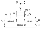
- Fig. 2 of the accompanying drawings shows diagrammatically a structure of a cell used in a flash memory.
- V G is a gate terminal, at V D a drain terminal, at V S a source terminal, at 27 a control gate CG connected to the gate terminal V G , and at 25 a floating gate FG which is controlled by the potential of the control gate CG.
- a semiconductor substrate e.g. a semiconductor substrate having P-type conductivity.
- well portions 23, 24 made of semiconductor having N-type conductivity.
- the well portion 23 forms a drain while the well portion 24 forms a source.
- Indicated at 26, 28 are insulating films.
- the write verification and erase verification are carried out so as to confirm whether the degree of writing and the degree of erasing have a sufficient margin for the read voltage, i.e., a variation range of the normal supply voltage V CC (5V ⁇ 0.5V). Generally, these verifications are carried out to confirm that an operation margin of about 0.5V to 1.0V is available for a voltage range of V CC . In this case, the verify voltage including the operation margin is 6V to 6.5V in the write verification, and 3.5V to 4V in the erase verification.
- the write verification and the erase verification can be accomplished easily if the verify voltage including the operation margin to be secured is applied to word lines (for example, word lines WL 1 to WL m of the flash memory shown in Fig. 1), so that the sensitivity of the S/A circuit is the same regardless of whether the voltage V CC or the verify voltage is applied as the supply voltage of the S/A circuit.
- word lines for example, word lines WL 1 to WL m of the flash memory shown in Fig. 1
- Fig. 3 of the accompanying drawings shows a construction of a general S/A circuit used in the non-volatile semiconductor memory such as an EPROM.
- V CC is a line of a supply voltage 5v
- V SS a line of a supply voltage 0V.
- a gate of the transistor 11 is connected to power supply line V SS
- a gate of the transistor 12 is connected to a data line (i.e., a bit line).
- a data line i.e., a bit line.
- an n-channel transistor 13 whose gate is connected to drains of the respective transistors 11, 12.
- a p-channel transistor 14 and an n-channel transistor 15 in series.
- a gate of the transistor 14 is connected to the power supply line V SS
- a gate of the transistor 15 is connected to the drains of the respective transistors 11, 12.
- An output (data output) of the S/A circuit is taken from drains of the respective transistors 14, 15.
- the transistor 15 is provided with a function of transmitting the level of the bit line to the data output line (bit line level adjustment), and the transistor 14 is provided with a function of discriminating the data of the memory cell according to the state (on/off) of the transistor 15.
- nonvolatile semiconductor memory of the prior art in the case where a number of continuous addresses (greater than the number of built-in sense amplifiers per bit) are accessed, there exists halfway a waiting time for an operation of the sense amplifier. Thus, it is impossible to read an output of a corresponding data at regular time intervals and at a high speed. It is desirable to overcome the defects residing in the prior art and to provide a nonvolatile semiconductor memory capable of reading a plurality of data stored in memory cell means at high speed and, particularly a nonvolatile semiconductor memory capable of reading continuous addresses at high speed and at regular time intervals.
- a semiconductor memory comprising first address generating means which is connected at least to address buffer means, memory cell means, word line selecting means, bit line selecting means, and an output buffer, and is adapted to designate one address to a group including a plurality of information; second address generating means for designating one address to each individual piece of information; first reading means selectively reading the plurality of information included in the group through either one of the word line selecting means and the bit line selecting means using one address value in the first address generating means; second reading means for selectively reading the individual information included in the group selectively read by the one address value in the first address generating means to the output buffer through either one of the bit line selecting means and the word line selecting means using address values in the second address generating means; and anticipatory reading means, i.e.
- pre-read means for reading a plurality of information included in another group corresponding to another address in a first address group using another address value in the first address generating means until the plurality of information read by the one address from the first address generating means is selectively read to the output buffer by the respective addresses in the second address generating means after the plurality of information is read by the one address in the first address generating means.
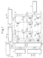
- Fig. 1 is a block diagram showing parts of a flash type memory.
- indicated at 1 is a cell array formed by arranging erasable nonvolatile memory cells M ij at intersections of a plurality of word lines WL 1 , to WL m and a plurality of bit lines BL 11 to BL 1k , ..., BL n1 to BL nk .
- the cell array is divided into n blocks, in each of which (k ⁇ m) memory cells are arranged.
- Indicated at 2 is a row address buffer for buffering a row address RAD of an address signal fed externally thereto, at 3 a row decoder for decoding the row address and selecting any one of the word lines WL 1 to WL m , at 4 a column address buffer for buffering a column address CAD of the address signal, and at 5 a column decoder for decoding the column address and selecting any one of column lines CL 1 to CL k corresponding to the bit lines BLi 1 to BLi k for each of the aforementioned blocks.
- Indicated at 6 is a column gate circuit including transfer gate transistors Q 1 to Q k corresponding to the bit lines BL i1 to BL ik for each of the aforementioned blocks. The respective transistors Q 1 to Q k are turned on when the corresponding column lines CL 1 to CL k are selected, to thereby connect the selected bit line BL ij to a data line D i .
- Indicated at 7 1 to 7 n are respectively writing circuits and S/A circuits for applying amplification to a write data and sense amplification to a read data between corresponding internal data lines D 1 to D n and external input/output data lines I/O 1 to I/O n .
- Indicated at 8 is a verify source voltage generating circuit for generating a verify voltage V VER in accordance with a control signal C fed externally thereto. The generated verify source voltage V VER is supplied to the selected word lines WL 1 to WL m through the row decoder 3 as described later, and to the S/A circuit corresponding to the selected word line.
- Indicated at 9 is a source voltage supply circuit for supplying a source voltage in common to the respective sources of the nonvolatile memory cells M ij .
- the device may employ a method which includes a plurality of sense amplifiers per bit and selects the output of the sense amplifiers by the address so that the data of a plurality of addresses can be read out in parallel with one another.
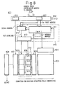
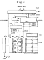
- Fig. 4 shows parts of a semiconductor memory device 801 according to the prior art.
- This device has an address buffer 802 for receiving an address input ADD inputted from a suitable external memory circuit, bit selection means 805, a sense amplifier 806, sense amplifier selection means 807 and an output buffer 808.
- the address buffer means 802 is provided with first address generation means for simultaneously making access to a predetermined number of data groups and reading them, and with second address generation means for individually selecting a plurality of data selected by the first address generation means.
- the first address generation means selects, for example, a predetermined word line from a plurality of word lines WL, and makes it possible to read out all of a plurality of data stored along the selected word line.
- the addressing information generated by the first address generation means is generally referred to as a "high order address".
- the second address generation means generates addresses for suitably and individually selecting the bit lines BL in order to select a plurality of data selected by the host address. These addresses are generally referred to as a "lower order address”.
- the read-out operation of the data by the first address generation means that is, by the higher order address
- the read-out operation of the selected data for each bit line BL by the second address generation means that is, by the lower order address
- selection of data by the higher order address is time-consuming, while selection of data by the lower order address under the state where the higher order address is fixed, that is, under the state where the higher order address does not change, can be carried out at random and at high speed.
- the access time becomes longer.
- the conventional semiconductor memory device 801 since a sense wait time exists in the conventional semiconductor memory device 801, the data read-out time is time-consuming. Therefore, the conventional semiconductor memory device is not suitable for high speed operation.
- an embodiment of the present invention seeks to provide a non-volatile semiconductor memory device which can eliminate the drawbacks of the prior art described above, and which can read out a plurality of data stored in memory cell means at a high speed.
- an embodiment of the present invention employs the following technical construction.
- the semiconductor memory device includes at least address buffer means, memory cell means, word line selection means, bit line selection means, output buffer, first address generation means for imparting one address to each group using a plurality of data as one group, and second address generation means for imparting one address to each of the individual data
- a non-volatile semiconductor memory device embodying the present invention employs the basic technical construction described above.
- the prior art employs a construction wherein, when the access is made to the memory cell means by the use of the higher order address to once output predetermined data to the output buffer and then makes once again the access to the memory cell means by the use of the next or other higher order address, the prior art makes the access to the memory cell means by the use of the higher order address to read out the predetermined data, and while the data is once written and stored in the sense amplifier, the prior art sets the sense wait time described above so that no operation is carried out in that period.
- an embodiment of the present invention utilizes this sense wait time for making access to the memory cell means in advance by the use of the next or other higher order address so as to read out the data corresponding to the address and to prepare for the next operation.
- the readout operation by the higher order address which will otherwise need a long time can be executed in advance, so as to improve the read-out speed of the data.
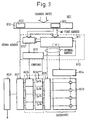
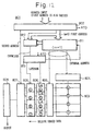
- FIG. 6 is a block diagram showing the semiconductor memory 801 according to the embodiment.
- the semiconductor memory 801 comprises address buffer means 802, memory cell means 803, word line selection means 804, bit line selection means 805, and an output buffer 808.
- the address buffer means 802 includes a first address generator 821 for generating an address to specify a group of data pieces, and a second address generator 822 for generating addresses to specify the data pieces within a specified group.
- the semiconductor memory 801 further comprises first read means 814 for selecting and reading a group of data pieces through the word line selection means 804 or the bit line selection means 805 according to an address provided by the first address generator 821; second read means 807 for selecting the data pieces, which have been selected and read according to the address provided by the first address generator 821 through the word line selection means 804 or the bit line selection means 805, according to addresses provided by the second address generator 822 and providing the output buffer 808 with the data pieces as selected (the second read means 807 may be sense amplifier selection means 807); and pre-read means 810 for reading another group of data pieces according to another address provided by the first address generator 821 while the preceding data pieces, which have been read according to the address provided by the first address generator 821, are being selected and provided to the output buffer 808 according to the addresses provided by the second address generator 822.
- first read means 814 for selecting and reading a group of data pieces through the word line selection means 804 or the bit line selection means 805 according to an address provided by the first address generator 8
- the semiconductor memory 801 of this embodiment basically resembles the conventional semiconductor memory 801 of Fig. 4.
- the semiconductor memory 801 of this embodiment is characterized by the pre-read means 810, which reads, during a sense wait time, a group of data pieces from the memory cell means 803 according to the next or another upper address and has the read data pieces on standby.
- the first address generator 821 in the embodiment generates an address for specifying, for example, a word line WL and bit lines BL corresponding to a group of different data pieces. Namely, the address provided by the first address generator 821 corresponds to a conventional upper address.
- the second address generator 822 in this embodiment generates addresses for selecting a data piece from amongst the group of data pieces selected by the first address generator 821.
- Each sense amplifier of the first read means outputs a data piece of the group and the output data output from the sense amplifier is selected by the sense amplifier selecting means 807.
- the address provided by the second address generator 822 correspond to conventional lower addresses.
- the first read means 814 may comprise sense amplifiers 806, or the sense amplifiers 806 and latch circuits 809.
- the pre-read means 810 in this embodiment includes an internal address generator 811 and a comparator 812.
- the internal address generator 811 has an input portion for receiving an address from the first address generator 821 of the address buffer means 802, and means such as a counter for changing an address held in the internal address generator 811 according to a given control signal.
- the comparator 812 compares an address provided by the internal address generator 811 with an address provided by the first address generator 821.
- the comparator 812 When the two addresses agree with each other, the comparator 812 provides a signal according to which the first read means 814 pre-reads a group of data pieces corresponding to the agreed address out of the memory cell means 803. At the same time, the comparator 812 provides the internal address generator 811 with a control signal. In response to the control signal, the internal address generator 811 changes a count of the counter (the address changing means), to provide a different address.
- This different address may be an increment or decrement of the preceding address, or a random address.
- the pre-read means 810 in this embodiment has a timing controller 813 for controlling the internal address generator 811 and comparator 812 in relation to one another.
- the timing controller 813 also controls the timing of the sense amplifiers 806 and latch circuits 809 of the first read means 814 as well as the timing of the sense amplifier selection means (the second read means) 807.
- the timing controller 813 is controlled by an address transition detector (not shown) that determines whether or not an address from the first address generator 821 has been changed and,when it has been changed, provides a signal ATD.
- Reading a group of data pieces according to an address provided by the internal address generator 811 from the memory cell means 803 into the sense amplifiers 806 of the first read means 814 involves a predetermined delay time.
- the pre-read means 810 uses this delay time, to access, in advance, an address that is different from the address now provided by the internal address generator 811.
- the timing controller 813 After the delay time, the timing controller 813 provides a latch signal. In response to the latch signal, the latch circuits 809 latch the data pieces from the sense amplifiers 806. At the same time, the timing controller 813 provides a signal for changing a count in the internal address generator 811.
- this embodiment accesses the next upper address while the present data are being read and delivered to the outside, to thereby solve the problems of the prior art.
- the embodiment employs the detector for detecting a change in an address provided by the first address generator 821, the counter (or an adder) 817 for incrementing an address according to an addition signal generated when the address change is detected, the comparator 812 for comparing the incremented address with an externally provided address, the latch circuits 809 for latching data pieces from the sense amplifiers 806, and the timing controller 813 for generating control signals for controlling the above-mentioned circuits according to predetermined timing.
- the comparator 812 compares this address with an incremented address provided by the internal address generator 811. If the addresses agree with each other, the latches 809 latch data from the sense amplifiers 806, and the latched data are delivered to the outside.
- the address in the internal address generator 811 is incremented to start the next access operation. This process is repeated to access continuous or random addresses at high speed.
- this embodiment can read data from consecutive addresses at high speed.
- the embodiment requires a small number of sense amplifiers in a chip, to thereby reduce the chip area and cost per bit.
- Figure 8 shows an initial state of the semiconductor memory 801.
- the first address generator 821 provides the comparator 812 and internal address generator 811 with an address m.
- the comparator 812 receives no internal address from the internal address generator 811, and therefore provides a disagreement signal.
- the first address generator 821 provides the address m at time T1.
- an address change detected signal ATD is provided to drive the comparator 812.
- a signal LOAD is provided at time t1 as there is no coincidence. Accordingly, at time t2, the external address m from the first address generator 821 is provided to and held by the internal address generator 811, as indicated with numeral 41.
- a word line m is selected according to the address m, and data pieces 0 to 3 corresponding to the word line m are read.
- a sense wait time S1 starts at time t3. During the sense wait time S1, the processing of the data pieces 0 to 3 of the address m is suspended.
- An access period 850 is of the preceding step. In this example, nothing is done during the access period 850 because the process has just started.
- a period 851 starts at time t4.
- the sense amplifiers 806 read the data pieces 0 to 3 from the address m.
- a latch signal R1 is provided at time t6, so that the latches 809 latch the data pieces 0 to 3 from the sense amplifiers 806 during a period 861.
- the signals LOAD and ATD, signals for the sense wait time S, and latch signal are provided through the timing controller 813.
- an addition signal A1 is provided at time t7.
- the address m in the internal address generator 811 is incremented, for example, by one to m+1, which is held therein during a period 42 starting at time t8.
- a word line m+1 is selected according to the address m+1, and data pieces 4 to 7 corresponding to the word line m+1 are read.
- the data pieces 0 to 3 latched by the latch circuits 809 are provided to the output buffer 808 through the sense amplifier selection means 807 sequentially or at random according to addresses provided by the second address generator 822.
- the sense amplifiers 806 read the data pieces 4 to 7 from the address m+1.
- the sense wait time S2 ends at time t12.
- the external address provided by the first address generator 821 becomes m+1.
- the address change detector accordingly provides the address change signal ATD at time t13.
- the comparator 812 carries out comparison.
- the comparator 812 determines that the address m+1 provided by the internal address generator 811 agrees with the external address m+1 provided by the first address generator 821, and provides an agreement signal IC.
- a latch signal R2 is provided at time t14, so that the latch circuits 809 latch the data pieces 4 to 7 from the sense amplifiers 806 during a period 862.
- an addition signal A2 is provided at time t15. Accordingly, the internal address generator 811 increments the currently-held address m+1 by one to m+2 and holds it during a period 43 starting from time t16.
- a word line m+2 is selected according to the address m+2, and data pieces 8 to 11 corresponding to the word line m+2 are read.
- the internal address generator 811 starts a pre-read access to the word line m+2.
- the data pieces 3 to 7 latched by the latch circuits 809 are provided to the output buffer 808 through the sense amplifier selection means 807 sequentially or at random according to addresses provided by the second address generator 822.
- the sense amplifiers 806 read the data pieces 8 to 11 from the address m+2.
- the sense wait time S3 ends at time t20.
- the external address provided by the first address generator 821 becomes m+2 at time T3. Accordingly, the address change detector provides an address change signal ATD at time t21. In response to the signal ATD, the comparator carries out comparison.
- the comparator 812 determines that the address m+2 provided by the internal address generator 811 agrees with the external address m+2 provided by the first address generator 821, and provides an agreement signal IC.
- a latch signal R3 is provided at time t23, so that the latch circuits 809 latch the data pieces 8 to 11 from the sense amplifiers 806 during a period 863.
- an addition signal A3 is provided at time t24. Accordingly, the internal address generator 811 increments the presently held address m+2 by one to m+3 and holds it during a period 44 starting at time t25. Similar to the previous case, the internal address generator 811 starts a pre-read access with the address m+3, to read data pieces 12 to 15 from a word line m+3.
- the data pieces 8 to 11 latched by the latch circuits 809 are provided to the output buffer 808 through the sense amplifier selection means 807 sequentially or at random according to addresses provided by the second address generator 822.
- this embodiment uses a sense wait time to pre-read memory cell means according to the next or another upper address and has data pieces corresponding to the address on standby.
- the pre-reading operation of the embodiment may be effective to improve a data read speed.
- the embodiment can read consecutive addresses at high speed.
- the embodiment requires a small number of sense amplifiers in a chip, to thereby reduce a chip area and cost per bit.
Landscapes
- Read Only Memory (AREA)
- Dram (AREA)
- Image Input (AREA)
- Techniques For Improving Reliability Of Storages (AREA)
Applications Claiming Priority (5)
| Application Number | Priority Date | Filing Date | Title |
|---|---|---|---|
| JP3346663A JP2732471B2 (ja) | 1991-12-27 | 1991-12-27 | 不揮発性半導体記憶装置 |
| JP34666391 | 1991-12-27 | ||
| JP32430292 | 1992-12-03 | ||
| JP32430292A JP3544678B2 (ja) | 1992-12-03 | 1992-12-03 | 半導体記憶装置 |
| EP92311829A EP0549374B1 (fr) | 1991-12-27 | 1992-12-29 | Mémoire non-volatile à semi-conducteur |
Related Parent Applications (1)
| Application Number | Title | Priority Date | Filing Date |
|---|---|---|---|
| EP92311829A Division EP0549374B1 (fr) | 1991-12-27 | 1992-12-29 | Mémoire non-volatile à semi-conducteur |
Publications (3)
| Publication Number | Publication Date |
|---|---|
| EP0933778A2 true EP0933778A2 (fr) | 1999-08-04 |
| EP0933778A3 EP0933778A3 (fr) | 1999-11-17 |
| EP0933778B1 EP0933778B1 (fr) | 2004-07-21 |
Family
ID=32774151
Family Applications (1)
| Application Number | Title | Priority Date | Filing Date |
|---|---|---|---|
| EP98121760A Expired - Lifetime EP0933778B1 (fr) | 1991-12-27 | 1992-12-29 | Mémoire à semiconducteur non volatile |
Country Status (2)
| Country | Link |
|---|---|
| EP (1) | EP0933778B1 (fr) |
| DE (1) | DE69233384T2 (fr) |
Family Cites Families (2)
| Publication number | Priority date | Publication date | Assignee | Title |
|---|---|---|---|---|
| US4156905A (en) * | 1974-02-28 | 1979-05-29 | Ncr Corporation | Method and apparatus for improving access speed in a random access memory |
| US4509142A (en) * | 1982-12-15 | 1985-04-02 | Texas Instruments Incorporated | Semiconductor memory device with pipeline access |
-
1992
- 1992-12-29 DE DE1992633384 patent/DE69233384T2/de not_active Expired - Fee Related
- 1992-12-29 EP EP98121760A patent/EP0933778B1/fr not_active Expired - Lifetime
Also Published As
| Publication number | Publication date |
|---|---|
| EP0933778A3 (fr) | 1999-11-17 |
| DE69233384T2 (de) | 2005-08-25 |
| EP0933778B1 (fr) | 2004-07-21 |
| DE69233384D1 (de) | 2004-08-26 |
Similar Documents
| Publication | Publication Date | Title |
|---|---|---|
| US7542339B2 (en) | Clock synchronized non-volatile memory device | |
| KR100609669B1 (ko) | 감지 시간 제어 장치 및 방법 | |
| JP3942342B2 (ja) | 多値データを記録する不揮発性メモリ | |
| US5491809A (en) | Smart erase algorithm with secure scheme for flash EPROMs | |
| US20040109352A1 (en) | Flash memory device having uniform threshold voltage distribution and method for verifying same | |
| US5579262A (en) | Program verify and erase verify control circuit for EPROM/flash | |
| JPH0917191A (ja) | 不揮発性半導体記憶装置 | |
| US5214605A (en) | Automatic erasing optimization circuit for an electrically erasable and programmable semiconductor memory and method thereof | |
| US6614683B1 (en) | Ascending staircase read technique for a multilevel cell NAND flash memory device | |
| US5801991A (en) | Deselected word line that floats during MLC programming of a flash memory | |
| US5400287A (en) | Method for erasing and verifying nonvolatile semiconductor memory device | |
| JP3662725B2 (ja) | 単一ビットセル及び多量ビットセル動作の同時的な遂行が可能な不揮発性半導体メモリ装置 | |
| US6937522B2 (en) | Nonvolatile semiconductor memory device | |
| US7031192B1 (en) | Non-volatile semiconductor memory and driving method | |
| JP3708912B2 (ja) | 半導体集積回路装置 | |
| KR100642911B1 (ko) | 페이지 버퍼 및 이를 이용한 플래쉬 메모리 소자의 검증방법 | |
| US8743621B2 (en) | Operating method in a non-volatile memory device | |
| US5617350A (en) | Flash memory system having reduced disturb and method | |
| JP4672673B2 (ja) | 半導体装置および半導体装置の制御方法 | |
| CN100557714C (zh) | 读取闪存装置的方法 | |
| JP2000137992A (ja) | フラッシュメモリ装置及びその検証方法 | |
| JP5085058B2 (ja) | プログラムの検証読み取り中に列スキャンを通じてプログラム時間を短縮させうるフラッシュメモリ装置のプログラム方法 | |
| US20050213388A1 (en) | Semiconductor device and method for writing data into the semiconductor device | |
| EP0933778B1 (fr) | Mémoire à semiconducteur non volatile | |
| JP2508888B2 (ja) | 不揮発性半導体記憶装置 |
Legal Events
| Date | Code | Title | Description |
|---|---|---|---|
| PUAI | Public reference made under article 153(3) epc to a published international application that has entered the european phase |
Free format text: ORIGINAL CODE: 0009012 |
|
| AC | Divisional application: reference to earlier application |
Ref document number: 549374 Country of ref document: EP |
|
| AK | Designated contracting states |
Kind code of ref document: A2 Designated state(s): DE FR GB IT |
|
| PUAL | Search report despatched |
Free format text: ORIGINAL CODE: 0009013 |
|
| AK | Designated contracting states |
Kind code of ref document: A3 Designated state(s): DE FR GB IT |
|
| RIC1 | Information provided on ipc code assigned before grant |
Free format text: 6G 11C 7/00 A |
|
| 17P | Request for examination filed |
Effective date: 20000105 |
|
| 17Q | First examination report despatched |
Effective date: 20010205 |
|
| GRAP | Despatch of communication of intention to grant a patent |
Free format text: ORIGINAL CODE: EPIDOSNIGR1 |
|
| GRAS | Grant fee paid |
Free format text: ORIGINAL CODE: EPIDOSNIGR3 |
|
| GRAA | (expected) grant |
Free format text: ORIGINAL CODE: 0009210 |
|
| AC | Divisional application: reference to earlier application |
Ref document number: 0549374 Country of ref document: EP Kind code of ref document: P |
|
| AK | Designated contracting states |
Kind code of ref document: B1 Designated state(s): DE FR GB IT |
|
| REG | Reference to a national code |
Ref country code: GB Ref legal event code: FG4D |
|
| REF | Corresponds to: |
Ref document number: 69233384 Country of ref document: DE Date of ref document: 20040826 Kind code of ref document: P |
|
| ET | Fr: translation filed | ||
| PLBE | No opposition filed within time limit |
Free format text: ORIGINAL CODE: 0009261 |
|
| STAA | Information on the status of an ep patent application or granted ep patent |
Free format text: STATUS: NO OPPOSITION FILED WITHIN TIME LIMIT |
|
| 26N | No opposition filed |
Effective date: 20050422 |
|
| PGFP | Annual fee paid to national office [announced via postgrant information from national office to epo] |
Ref country code: GB Payment date: 20071227 Year of fee payment: 16 Ref country code: FR Payment date: 20071210 Year of fee payment: 16 |
|
| PGFP | Annual fee paid to national office [announced via postgrant information from national office to epo] |
Ref country code: IT Payment date: 20071228 Year of fee payment: 16 Ref country code: DE Payment date: 20071231 Year of fee payment: 16 |
|
| GBPC | Gb: european patent ceased through non-payment of renewal fee |
Effective date: 20081229 |
|
| REG | Reference to a national code |
Ref country code: FR Ref legal event code: ST Effective date: 20090831 |
|
| PG25 | Lapsed in a contracting state [announced via postgrant information from national office to epo] |
Ref country code: DE Free format text: LAPSE BECAUSE OF NON-PAYMENT OF DUE FEES Effective date: 20090701 |
|
| PG25 | Lapsed in a contracting state [announced via postgrant information from national office to epo] |
Ref country code: GB Free format text: LAPSE BECAUSE OF NON-PAYMENT OF DUE FEES Effective date: 20081229 |
|
| PG25 | Lapsed in a contracting state [announced via postgrant information from national office to epo] |
Ref country code: FR Free format text: LAPSE BECAUSE OF NON-PAYMENT OF DUE FEES Effective date: 20081231 |
|
| PG25 | Lapsed in a contracting state [announced via postgrant information from national office to epo] |
Ref country code: IT Free format text: LAPSE BECAUSE OF NON-PAYMENT OF DUE FEES Effective date: 20081229 |