EP0933800A2 - Système d'affichage cyclotron - Google Patents
Système d'affichage cyclotron Download PDFInfo
- Publication number
- EP0933800A2 EP0933800A2 EP99102142A EP99102142A EP0933800A2 EP 0933800 A2 EP0933800 A2 EP 0933800A2 EP 99102142 A EP99102142 A EP 99102142A EP 99102142 A EP99102142 A EP 99102142A EP 0933800 A2 EP0933800 A2 EP 0933800A2
- Authority
- EP
- European Patent Office
- Prior art keywords
- cyclotron
- electron
- screen
- cyclotrons
- electron beams
- Prior art date
- Legal status (The legal status is an assumption and is not a legal conclusion. Google has not performed a legal analysis and makes no representation as to the accuracy of the status listed.)
- Withdrawn
Links
Images




Classifications
-
- H—ELECTRICITY
- H01—ELECTRIC ELEMENTS
- H01J—ELECTRIC DISCHARGE TUBES OR DISCHARGE LAMPS
- H01J31/00—Cathode ray tubes; Electron beam tubes
-
- H—ELECTRICITY
- H01—ELECTRIC ELEMENTS
- H01J—ELECTRIC DISCHARGE TUBES OR DISCHARGE LAMPS
- H01J29/00—Details of cathode-ray tubes or of electron-beam tubes of the types covered by group H01J31/00
- H01J29/46—Arrangements of electrodes and associated parts for generating or controlling the ray or beam, e.g. electron-optical arrangement
- H01J29/48—Electron guns
-
- H—ELECTRICITY
- H01—ELECTRIC ELEMENTS
- H01J—ELECTRIC DISCHARGE TUBES OR DISCHARGE LAMPS
- H01J29/00—Details of cathode-ray tubes or of electron-beam tubes of the types covered by group H01J31/00
- H01J29/02—Electrodes; Screens; Mounting, supporting, spacing or insulating thereof
- H01J29/04—Cathodes
-
- H—ELECTRICITY
- H01—ELECTRIC ELEMENTS
- H01J—ELECTRIC DISCHARGE TUBES OR DISCHARGE LAMPS
- H01J29/00—Details of cathode-ray tubes or of electron-beam tubes of the types covered by group H01J31/00
- H01J29/46—Arrangements of electrodes and associated parts for generating or controlling the ray or beam, e.g. electron-optical arrangement
- H01J29/58—Arrangements for focusing or reflecting ray or beam
- H01J29/62—Electrostatic lenses
-
- H—ELECTRICITY
- H01—ELECTRIC ELEMENTS
- H01J—ELECTRIC DISCHARGE TUBES OR DISCHARGE LAMPS
- H01J3/00—Details of electron-optical or ion-optical arrangements common to two or more basic types of discharge tubes or lamps
- H01J3/02—Electron guns
Definitions
- the described invention is an apparatus for display of images on a Screen.
- the cyclotron display comprises one or more cyclotrons used to produce and accelerate beams of electrons. Deflection mechanisms then direct the electrons toward a phosphor-coated screen which lights up with images.
- the invention is meant to be a substitute for the cathode ray tube (CRT) and can be used in the same array of machines that the CRT is used for, including, for example, oscilloscopes, computer monitors and television screens.
- CTR cathode ray tube
- the conventional CRT is a ubiquitous device that is used to display images in a variety of instruments.
- the CRT includes a cathode as an electron source.
- the cathode is heated, which causes it to emit a cloud of low-energy electrons. Focusing electrodes narrow this cloud into a beam, control electrodes ensure that the beam flows through the device at an appropriate rate, and accelerating electrodes accelerate the electrons to the requisite energy level (about ,500eV to 1500eV for low-voltage phosphor screens).
- the cathode and the accompanying electrodes described above are together commonly referred to as an "electron gun.”
- the beam of electrons then strikes a phosphor-coated screen, which causes the phosphor to emit light. This light produces coherent images because the electrons are appropriately deflected by deflecting electrodes before they strike the screen.
- Deflection of the electron beam is effected by two sets of orthogonal deflectors; one that deflects the beam horizontally, and one that deflects the beam vertically.
- the angle of deflection that can be achieved is proportional to the voltage applied to the deflecting electrodes and inversely proportional to the energy of the beam.
- the CRT has significant limitations in terms of power consumption, cost and size.
- the electron-producing cathode is a high-voltage, high-power device that nonetheless emits electrons in a diffuse cloud with low energy.
- the electron cloud must be focused and accelerated into a fast, tight beam to be useful. This requires the use of focusing electrodes as well as accelerating electrodes, both of which, but especially the latter, contribute to the high-energy consumption of the CRT.
- a long CRT tube is necessary to take advantage of the deflection angle imparted by deflection electrodes (a longer tube means that the electrons will be deflected a greater absolute distance). This problem can be off-set by an increase in the voltage of the deflecting electrodes, but this of course is not an ideal alternative.
- the described invention overcomes the above-mentioned and other limitations of conventional CRT technology by replacing the electron gun assembly of the CRT with one or more cyclotrons, which can produce electrons using lower voltages and less energy than the cathode of the electron gun.
- the electrons initially emerge from the cyclotron with adequate velocity they do not need to be further accelerated with accelerating electrodes. And because they emerge as electron beams, very little or even no focusing by focusing electrodes is required.
- an array of cyclotrons rather than just a single one, can be used to provide the needed electron beams for a screen.
- each individual cyclotron will be mapped to a fractional portion of the screen, the necessary deflection distance will be lessened, which in turn reduces the length of the device. It is worth noting that an array of electron beam sources could be used in a conventional CRT as well, in order to reduce the length of that device.
- the disclosed invention thus provides for economical, low-energy, flat panel displays with large screen dimensions.
- the cyclotron display like the conventional CRT, is evacuated to facilitate delivery of the electron beams with minimal disruption and loss of energy.
- Every embodiment of the cyclotron display includes at least one cyclotron.
- the cyclotron is a common device used to accelerate subatomic and atomic particles.
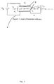
- the cyclotron 1 resembles a flat metal disk (see Figure 1).
- the metal disk comprises two metal halves called dees 2, because of their resemblance to the shape of that letter.
- the dees 2 are separated by a small empty space or gap. An electric field is generated in the vicinity of this empty space, resulting in a voltage drop across the gap.
- a uniform magnetic field perpendicular to the plane of the cyclotron and its dees 2 is generated by a pair of magnets 3 (either permanent magnets or Helmholtz coils) that are placed on either side of the dees (see Figure 1).
- a small electron source 4 comprising a thermionic metal-oxide covered cathode or point-discharge cathode, is placed in the center of the cyclotron.
- the electrons that are emitted from the electron source circulate in the direction of the circumference of the dees because the perpendicular magnetic field keeps them flowing in this direction.
- As an electron emerges into the gap between the dees it will experience the voltage drop across the gap, and so accelerate into the other dee, thus picking up velocity and energy.
- the electron will then be shielded from the electric field by the metal walls of the dee until it emerges into the gap again.
- the potential difference between the dees is purposefully reversed, so that the electron will accelerate into the other dee. This process is repeated until the electron is moving fast enough to emerge from the cyclotron aperture 5, when it has reached the "terminal radius" (see Figure 1).
- the electron will continue to accelerate in ever widening circles through the cyclotron until it has reached the terminal radius ( r term ) and terminal velocity ( ⁇ term ), where the radius of the orbit matches the radius of the cyclotron aperture.
- r term m ⁇ ⁇ term q ⁇ B
- the electron energy, T req can be determined by :
- the electron sources can be placed within one cyclotron.
- the electron sources may comprise several thermionic or point-discharge cathodes, or a single long cathode with multiple pointed protrusions.
- the electron sources 4 are strung out along one dimension, perpendicular to the plane of the dees 2 (see Figure 2).
- This type of cyclotron 1 has a cylindrical shape and produces multiple electron beams.
- This type of cyclotron 1 can replace multiple cyclotrons with single electron sources, and so replace all or part of an array of cyclotrons (see Examples 7-10 below).
- the electron beam After emerging from the cyclotron aperture, the electron beam is deflected by either magnetic or electrostatic deflectors, just as it would be if it were emerging from a conventional electron gun.
- a magnetic deflector is simply a magnetic coil.
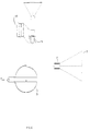
- An electrostatic deflector 6 is a pair of electrostatic plates 7 with a voltage between them (see Figure 3).
- E V def / d ⁇
- V def the voltage
- d ⁇ the distance between the plates.
- the distance between the deflector and the screen, d will need to be only 12cm to achieve this velocity.
- the entire cyclotron display unit can be made under 15cm.
- a 20V deflector will reduce the distance to 6cm, which means the display unit can be reduced to 10cm in length.
- the potential for flat-screen cyclotron display devices is made clear by these sample calculations. These and other sample calculations are tabulated in Figure 4.
- Monochrome Display Unit Comprising a Single Cyclotron and Producing a Single Electron Beam
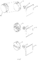
- This embodiment of the invention comprises a single cyclotron (see Figures 5 and 6).
- the cyclotron 1 produces a single beam which is appropriately deflected by a deflection unit 8.
- the electron beam sweeps across phosphor screen 9, in this example a monochrome screen, and strikes the appropriate pixels on that screen to create images, just as it would in a conventional CRT.
- Methods for controlling deflection of the electron beam to create images on a monochrome display screen are the same as those used in conventional CRT displays, and are well known in the art.
- a general description of this art is contained in, e.g., Robert A. Meyers, ed., Encyclopedia of Physical Science and Technology, Second Edition, Vol, 5 , pp. 695-701, Academic Press (San Diego, 1992) and Jerry C. Whitaker, ed., The Electronics Handbook , pp. 367-386, CRC Press, Inc. (Beaverton, 1996).
- This embodiment of the invention comprises a single cyclotron (see Figure 7).
- the cyclotron 1 produces a bundle of three electron beams (by one electron source 4 generating three pulses very close in time, or by three separate electron sources 4) which is deflected by a single deflection unit 8 and then strikes the phosphor screen 9, in this example a color screen.
- the phosphor screen 9 is of the same type used in a conventional CRT.
- Each pixel 10 on the phosphor screen 9 will contain a red, green and blue phosphor dot, either in delta arrangement, or in parallel arrangement (such as with the Sony TrinitronTM display).
- This embodiment of the invention comprises a set of three cyclotrons 11 (see Figures 5 and 6).
- the set of three cyclotrons 11 together produce a bundle of three electron beams (one beam from each cyclotron) which is deflected by a single deflection unit 8, or by three separate deflection units (not shown), and then strikes the color phosphor screen 9.
- Methods for controlling deflection of the electron beam to create images on a color display screen are the same as those used in conventional CRT display, and are well known in the art, as described in Example 2.
- Monochrome Display Unit Comprising an Array of Cyclotrons Each Producing a Single Electron Beam
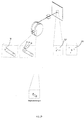
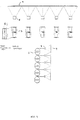
- This embodiment of the invention comprises an array of cyclotrons (see Figures 8 and 9).
- Each cyclotron 1 produces a single beam which is deflected by a separate deflection unit 8 and then strikes the monochrome phosphor screen 9.
- Each cyclotron 1 and each beam maps to a fractional portion 12 of the screen.
- Methods for controlling deflection of the electron beam to create images on a monochrome display screen are the same as those used in conventional CRT display, and are well known in the art, as described in Example 1.
- the incoming video signal must at some point be processed so that it can be appropriately distributed among the cyclotrons in the array.
- This process which is essentially a form of demultiplexion, can be done in combination with a memory chip that temporarily stores the signal (after digitization, if it is an analog signal).
- Signal demultiplexing is well known in the art. A general description of demultiplexing is contained in, e.g., Paul Horowitz and Winfred Hill, eds., The Art of Electronics. Second Edition , pp. 490-504, Cambridge University Press (Cambridge, England, 1989), especially pp.
- Video wall displays contain processors that divide an image intended for a single monitor among several monitors stacked together into an array or wall. This type of signal processing is well-known in the art, as taught in, e.g., U.S. Patent 5,130,794, U.S. Patent 4,635,105 and U.S. Patent 4,563,703.
- This embodiment of the invention comprises an array of cyclotrons (see Figures 8 and 9).
- Each cyclotron 1 produces a bundle of three electron beams (by one electron source 4 generating three pulses very close in time, or by three separate electron sources 4) which is deflected by a single deflection unit 8 and then strikes the color phosphor screen 9, just as in Example 2, except that each cyclotron 1 and each bundle maps to a fractional portion 12 of the screen, just as in Example 4.
- the incoming video signal must at some point be processed so that it can be appropriately distributed among the cyclotrons in the array. This process is described in Example 4.
- This embodiment of the invention comprises an array of sets of three cyclotrons 11 (see Figures 8 and 9).
- Each cyclotron set 11 produces a bundle of three electron beams that strikes the color screen 9 just as in Example 5, where each three cyclotron set 11 and each bundle maps to a fractional portion 12 of the screen.
- Each bundle is deflected by a single deflection unit 8 or by three separate deflection units (not shown).
- the incoming video signal must at some point be processed so that it can be appropriately distributed among the cyclotrons in the array. This process is described in Example 4.
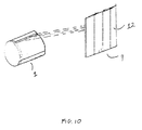
- This embodiment of the invention comprises a cyclotron comprising multiple electron sources along one dimension (see Figure 10).
- the cyclotron 1 emits multiple electron beams through the cyclotron aperture 5.
- the electron beams then strike the monochrome screen 9, and each electron source 4 and each electron beam maps to a fractional portion 12 of the screen, just as in Example 4.
- the incoming video signal must at some point be processed so that it can be appropriately distributed among the electron sources in the cyclotron. This process is described in Example 4.
- This embodiment of the invention comprises a cyclotron comprising multiple electron sources along one dimension (see Figure 10).
- the cyclotron 1 emits multiple bundles of electron beams through the cyclotron aperture 5, each bundle being produced by a single electron source or by three electron sources.
- the bundles of electron beams then strike the color screen 9, and each bundle of electron beams maps to a fractional portion 12 of the screen, just as in Example 5.
- the incoming video signal must at some point be processed so that it can be appropriately distributed among the electron sources in the cyclotron. This process is described in Example 4.
- Monochrome Display Unit Comprising an Array of Cylindrical Cyclotrons
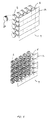
- This embodiment of the invention comprises an array of cyclotrons comprising multiple electron sources along one dimension (see Figure 11).
- the embodiment comprises one or more cyclotrons along one dimension and multiple cyclotrons along another.
- the cyclotrons 1 emit multiple electron beams through their cyclotron apertures 5.
- the electron beams then strike the monochrome screen 9, and each electron source and each electron beam maps to a fractional portion 12 of the screen, just as in Example 4.
- the incoming video signal must at some point be processed so that it can be appropriately distributed among all the electron sources in all the cyclotrons. This process is described in Example 4.
- This embodiment of the invention comprises an array of cyclotrons comprising multiple electron sources along one dimension (see Figure 11).
- the embodiment comprises one or more cyclotrons along one dimension and multiple cyclotrons along another.
- the cyclotrons 1 emit multiple bundles of three electron beams through their cyclotron apertures 5, each bundle being produced by a single electron source or by three electron sources.
- the electron beams then strike the color screen 9, and each bundle of electron beams maps to a fractional portion 12 of the screen, just as in Example 5.
- the incoming video signal must at some point be processed so that it can be appropriately distributed among all the electron sources in all the cyclotrons. This process is described in Example 4.
Landscapes
- Cathode-Ray Tubes And Fluorescent Screens For Display (AREA)
- Particle Accelerators (AREA)
Applications Claiming Priority (2)
| Application Number | Priority Date | Filing Date | Title |
|---|---|---|---|
| US18219 | 1998-02-03 | ||
| US09/018,219 US6144143A (en) | 1998-02-03 | 1998-02-03 | Cyclotron displays |
Publications (2)
| Publication Number | Publication Date |
|---|---|
| EP0933800A2 true EP0933800A2 (fr) | 1999-08-04 |
| EP0933800A3 EP0933800A3 (fr) | 2001-05-16 |
Family
ID=21786851
Family Applications (1)
| Application Number | Title | Priority Date | Filing Date |
|---|---|---|---|
| EP99102142A Withdrawn EP0933800A3 (fr) | 1998-02-03 | 1999-02-03 | Système d'affichage cyclotron |
Country Status (6)
| Country | Link |
|---|---|
| US (1) | US6144143A (fr) |
| EP (1) | EP0933800A3 (fr) |
| JP (1) | JPH11273595A (fr) |
| KR (1) | KR19990072401A (fr) |
| CN (1) | CN1237872A (fr) |
| TW (1) | TW439079B (fr) |
Families Citing this family (2)
| Publication number | Priority date | Publication date | Assignee | Title |
|---|---|---|---|---|
| NL1036912C2 (en) * | 2009-04-29 | 2010-11-01 | Mapper Lithography Ip Bv | Charged particle optical system comprising an electrostatic deflector. |
| JP5606793B2 (ja) * | 2010-05-26 | 2014-10-15 | 住友重機械工業株式会社 | 加速器及びサイクロトロン |
Family Cites Families (10)
| Publication number | Priority date | Publication date | Assignee | Title |
|---|---|---|---|---|
| US2242888A (en) * | 1938-02-16 | 1941-05-20 | Telefunken Gmbh | Ultra short wave oscillation generator |
| US2243041A (en) * | 1938-05-07 | 1941-05-20 | Hygrade Sylvania Corp | Television tube |
| FR1444190A (fr) * | 1965-05-20 | 1966-07-01 | Cft Comp Fse Television | Perfectionnements aux tubes récepteurs de télévision en couleurs |
| US3411029A (en) * | 1966-04-04 | 1968-11-12 | Richard D. Karr | Color television picture tube |
| GB8306339D0 (en) * | 1982-03-19 | 1983-04-13 | Quantel Ltd | Video processing systems |
| FR2549671B1 (fr) * | 1983-07-22 | 1987-05-22 | Thomson Csf | Dispositif d'affichage d'une image de television de grandes dimensions et recepteur de television comportant un tel dispositif |
| KR900000351B1 (ko) * | 1984-05-10 | 1990-01-25 | 가부시끼가이샤 도시바 | 컬러 수상관장치 |
| US4792720A (en) * | 1985-12-09 | 1988-12-20 | Kabushiki Kaisha Toshiba | Color cathode ray tube |
| US5130794A (en) * | 1990-03-29 | 1992-07-14 | Ritchey Kurtis J | Panoramic display system |
| US5712525A (en) * | 1993-05-19 | 1998-01-27 | Hull; Otis E. | Shadow mask for a mutltiple element cathode ray tube |
-
1998
- 1998-02-03 US US09/018,219 patent/US6144143A/en not_active Expired - Fee Related
- 1998-03-20 TW TW087104138A patent/TW439079B/zh not_active IP Right Cessation
-
1999
- 1999-02-03 JP JP11026762A patent/JPH11273595A/ja not_active Withdrawn
- 1999-02-03 CN CN99103040A patent/CN1237872A/zh active Pending
- 1999-02-03 KR KR1019990003643A patent/KR19990072401A/ko not_active Withdrawn
- 1999-02-03 EP EP99102142A patent/EP0933800A3/fr not_active Withdrawn
Also Published As
| Publication number | Publication date |
|---|---|
| TW439079B (en) | 2001-06-07 |
| US6144143A (en) | 2000-11-07 |
| CN1237872A (zh) | 1999-12-08 |
| JPH11273595A (ja) | 1999-10-08 |
| KR19990072401A (ko) | 1999-09-27 |
| EP0933800A3 (fr) | 2001-05-16 |
Similar Documents
| Publication | Publication Date | Title |
|---|---|---|
| KR950010036B1 (ko) | 평면 영상 디스플레이장치 | |
| AU647738B2 (en) | Thin-type picture display device | |
| US4069439A (en) | Flat panel display with beam injection cleanup | |
| US5347199A (en) | Thin-type picture display device with means for effecting electron transport by secondard emission | |
| WO1985005491A1 (fr) | Affichage a panneau plat utilisant un reseau lineaire de cathodes d'emission de champ | |
| US5130614A (en) | Ribbon beam cathode ray tube | |
| US6144143A (en) | Cyclotron displays | |
| JPH04163833A (ja) | 画像表示装置 | |
| US5189335A (en) | Method of controlling electron beams in an image display apparatus | |
| JPS61234183A (ja) | フラツトスクリ−ンcrtの走査方式 | |
| JPS6049540A (ja) | 陰極線管装置 | |
| US6515639B1 (en) | Cathode ray tube with addressable nanotubes | |
| US5990609A (en) | Display device with resistive anodes | |
| US5877597A (en) | Display device | |
| US4215293A (en) | Cadence scanned flat image display device | |
| KR100290250B1 (ko) | 표시장치 | |
| KR100545713B1 (ko) | 플랫 브라운관 구조체 | |
| HK1024137A (en) | Cyclotron displays | |
| KR930007368B1 (ko) | 화상표시장치에 있어서의 전자비임의 제어방법 | |
| JP3125598B2 (ja) | 平板型画像表示装置 | |
| US4137485A (en) | Image display block scanning method | |
| US4705985A (en) | Cathode-ray tube and electron gun structure therefor | |
| JPH08186843A (ja) | 立体画像表示装置 | |
| JPH01241742A (ja) | 画像表示装置 | |
| JPS58197642A (ja) | 画像表示装置 |
Legal Events
| Date | Code | Title | Description |
|---|---|---|---|
| PUAI | Public reference made under article 153(3) epc to a published international application that has entered the european phase |
Free format text: ORIGINAL CODE: 0009012 |
|
| AK | Designated contracting states |
Kind code of ref document: A2 Designated state(s): AT BE CH CY DE DK ES FI FR GB GR IE IT LI LU MC NL PT SE |
|
| AX | Request for extension of the european patent |
Free format text: AL;LT;LV;MK;RO;SI |
|
| PUAL | Search report despatched |
Free format text: ORIGINAL CODE: 0009013 |
|
| AK | Designated contracting states |
Kind code of ref document: A3 Designated state(s): AT BE CH CY DE DK ES FI FR GB GR IE IT LI LU MC NL PT SE |
|
| AX | Request for extension of the european patent |
Free format text: AL;LT;LV;MK;RO;SI |
|
| 17P | Request for examination filed |
Effective date: 20011114 |
|
| AKX | Designation fees paid |
Free format text: AT BE CH CY DE DK ES FI FR GB GR IE IT LI LU MC NL PT SE |
|
| STAA | Information on the status of an ep patent application or granted ep patent |
Free format text: STATUS: THE APPLICATION HAS BEEN WITHDRAWN |
|
| 18W | Application withdrawn |
Withdrawal date: 20020923 |