EP0933814A1 - Metallisierungsstruktur auf einem fluorhaltigen Dielektrikum und Herstellungsverfahren dafür - Google Patents
Metallisierungsstruktur auf einem fluorhaltigen Dielektrikum und Herstellungsverfahren dafür Download PDFInfo
- Publication number
- EP0933814A1 EP0933814A1 EP98870163A EP98870163A EP0933814A1 EP 0933814 A1 EP0933814 A1 EP 0933814A1 EP 98870163 A EP98870163 A EP 98870163A EP 98870163 A EP98870163 A EP 98870163A EP 0933814 A1 EP0933814 A1 EP 0933814A1
- Authority
- EP
- European Patent Office
- Prior art keywords
- layer
- fluorine
- barrier layer
- recited
- conductive pattern
- Prior art date
- Legal status (The legal status is an assumption and is not a legal conclusion. Google has not performed a legal analysis and makes no representation as to the accuracy of the status listed.)
- Withdrawn
Links
Images
Classifications
-
- H—ELECTRICITY
- H10—SEMICONDUCTOR DEVICES; ELECTRIC SOLID-STATE DEVICES NOT OTHERWISE PROVIDED FOR
- H10W—GENERIC PACKAGES, INTERCONNECTIONS, CONNECTORS OR OTHER CONSTRUCTIONAL DETAILS OF DEVICES COVERED BY CLASS H10
- H10W20/00—Interconnections in chips, wafers or substrates
- H10W20/40—Interconnections external to wafers or substrates, e.g. back-end-of-line [BEOL] metallisations or vias connecting to gate electrodes
- H10W20/41—Interconnections external to wafers or substrates, e.g. back-end-of-line [BEOL] metallisations or vias connecting to gate electrodes characterised by their conductive parts
- H10W20/425—Barrier, adhesion or liner layers
-
- H—ELECTRICITY
- H10—SEMICONDUCTOR DEVICES; ELECTRIC SOLID-STATE DEVICES NOT OTHERWISE PROVIDED FOR
- H10W—GENERIC PACKAGES, INTERCONNECTIONS, CONNECTORS OR OTHER CONSTRUCTIONAL DETAILS OF DEVICES COVERED BY CLASS H10
- H10W20/00—Interconnections in chips, wafers or substrates
- H10W20/40—Interconnections external to wafers or substrates, e.g. back-end-of-line [BEOL] metallisations or vias connecting to gate electrodes
- H10W20/41—Interconnections external to wafers or substrates, e.g. back-end-of-line [BEOL] metallisations or vias connecting to gate electrodes characterised by their conductive parts
- H10W20/42—Vias, e.g. via plugs
-
- H—ELECTRICITY
- H10—SEMICONDUCTOR DEVICES; ELECTRIC SOLID-STATE DEVICES NOT OTHERWISE PROVIDED FOR
- H10W—GENERIC PACKAGES, INTERCONNECTIONS, CONNECTORS OR OTHER CONSTRUCTIONAL DETAILS OF DEVICES COVERED BY CLASS H10
- H10W20/00—Interconnections in chips, wafers or substrates
- H10W20/40—Interconnections external to wafers or substrates, e.g. back-end-of-line [BEOL] metallisations or vias connecting to gate electrodes
- H10W20/41—Interconnections external to wafers or substrates, e.g. back-end-of-line [BEOL] metallisations or vias connecting to gate electrodes characterised by their conductive parts
- H10W20/44—Conductive materials thereof
- H10W20/4403—Conductive materials thereof based on metals, e.g. alloys, metal silicides
- H10W20/4421—Conductive materials thereof based on metals, e.g. alloys, metal silicides the principal metal being copper
- H10W20/4424—Copper alloys
-
- H—ELECTRICITY
- H10—SEMICONDUCTOR DEVICES; ELECTRIC SOLID-STATE DEVICES NOT OTHERWISE PROVIDED FOR
- H10W—GENERIC PACKAGES, INTERCONNECTIONS, CONNECTORS OR OTHER CONSTRUCTIONAL DETAILS OF DEVICES COVERED BY CLASS H10
- H10W20/00—Interconnections in chips, wafers or substrates
- H10W20/40—Interconnections external to wafers or substrates, e.g. back-end-of-line [BEOL] metallisations or vias connecting to gate electrodes
- H10W20/45—Interconnections external to wafers or substrates, e.g. back-end-of-line [BEOL] metallisations or vias connecting to gate electrodes characterised by their insulating parts
- H10W20/48—Insulating materials thereof
Definitions
- the present invention is related to a new metallization structure being part of a structure used to interconnect electronic components or devices. Such components or devices can be part of an integrated circuit. Particularly, a multi-level Cu-containing metallization structure is disclosed based on fluorine-containing dielectrics.
- a low material, a low K material and a material with a low permittivity are all alternative expressions for a material with a low dielectric constant, at least for the purposes of this disclosure.
- the most desirable material should have a low K value, low mechanical stress, high thermal stability and low moisture absorption.
- the desired material should be selected based on the compatibility with state-of-the-art semiconductor processing steps and tools.
- PECVD Plasma Enhanced Chemical Vapour Deposition
- the organic spin-on materials having a K value in the range from 2.5 to 3
- the inorganic low-K materials as e.g. xerogels having a K value typically lower than 1.5.
- Many of these new low-K materials comprise fluorine.
- the organic materials are of particular interest because they feature simplified processing, excellent gap-fill and planarization.
- the K-value of organic materials, which comprise Phenyl groups can be additionally lowered by plasma fluorination as e.g. in H. Kudo et al., Mat. Res. Symp. Proc., Vol. 381, pp. 105-110, 1985. By doing so the K-values can be lowered yielding a range from 2 to 2.5 instead of from 2.5 to 3.
- fluorinated dielectrics have in general a lower K-value than their unfluorinated counterparts. This holds both for polymer like and ceramic like dielectrics. Therefore fluorinated dielectrics are of particular interest in order to avoid that the larger portion of the total circuit delay is caused by the capacitance of the interconnect system. Despite all these advantages fluorinated dielectrics are not compatible with current metallization structures using metallization materials such as Ti, or Ta, or W, or the nitrides of each of the aforementioned materials, or Cu, or Al. This is due to the fact that the incorporation of fluorine has been shown to be detrimental for the aforementioned metallization materials.
- a contact barrier layer has to be provided which is at least conductive and impermeable for fluorine. Furthermore, preferably this layer is impermeable for Cu and forms a silicide when contacting a silicon substrate.
- a metallization structure comprising a barrier layer, said barrier layer being formed on the exposed parts, i.e. the uncovered parts, of a fluorinated dielectric.
- This barrier layer should adhere well on said fluorinated dielectric.
- This barrier layer should also neither corrode nor reveal a deterioration of its characteristics by the exposure to a fluorine.
- this barrier layer should also form a diffusion barrier for fluorine, by forming stable non-volatile fluorides, in order to inhibit the corrosion of other parts of the metallization structure.
- a conductive contact layer has to be provided. This contact layer contacts both the exposed parts of a substrate and the fluorinated dielectric.
- a conductive contact layer has to provide a low-ohmic contact to the exposed parts, i.e. the uncovered parts, of the substrate.
- a layer combining the requirements of both a barrier layer and a conductive contact layer is mentioned as a contact barrier layer hereafter.
- a metallization structure comprising:
- a metallization structure comprising a contact barrier layer, said layer containing a near noble metal as a material.
- a near noble metal is used.
- Co is much less reactive than the refractory metals.
- Co adheres well on silicon oxide based materials and polymers.
- a silicide-cobalt is defined as CoxSiy, x and y being positive numbers.
- the fluorides of Co are stable and non-volatile, i.e. contrary to e.g. Ti.
- Co reacts readily with fluorine thereby forming an in-situ cobalt-fluoride layer, i.e. a first sub-layer.
- the growth of this cobalt-fluoride layer is self-limiting resulting in a maximum thickness of the layer of about 5 nm. Consequently, contrary to e.g. Ti which is permeable for fluorine, by the reaction of Co or another near noble metal, such as Ni, Pd or Pt, with a fluorinated dielectric a layer of a fluoride of this near noble metal is formed.
- This layer inhibits the out-diffusion of fluorine from said fluorinated dielectric and thereby avoids the exposure of other parts of the metallization structure to fluorine.
- a metallization structure where the conductive pattern is composed of at least one metal selected from a group comprising Al, Cu, an Al-alloy and a Cu-alloy. Particularly, a Cu-containing metals is selected.
- This metallization structure can further comprise a barrier layer, impermeable for copper, being positioned between said conductive pattern and said contact barrier layer.
- this barrier layer is a Ta layer or a compound thereof.
- a metallization structure is disclosed, further comprising a second part of said contact barrier layer, being positioned between the substrate and said conductive pattern, said second part containing at least one sub-layer; and wherein said second part is in contact with said substrate.
- the substrate can be at least a part of a silicon wafer.
- the second part of said contact barrier layer comprises a first sub-layer containing said material, e.g. Co or another near noble material, and a second sub-layer of a silicide of said material, e.g. a silicide-cobalt, said second sub-layer contacting said substrate.
- a method for fabricating a metallization structure on a substrate comprising the steps of:
- a method is disclosed to fabricate a metallization structure, wherein prior to the formation of the conductive pattern, preferably composed of Cu or a Cu-alloy, a first barrier layer is deposited on the contact barrier layer to prevent the out-diffusion of Cu.
- this first barrier layer is a layer comprising Ta or a compound thereof.
- a method is disclosed to fabricate a metallization structure, wherein after the formation of the conductive pattern a second barrier layer is deposited at least on said conductive pattern.
- said second barrier layer can contain an element selected from a group comprising Co, Ni, Pt, Pd, Ti, Ta or a compound of one of the previous elements.
- a metallization structure which is compatible with said fluorinated dielectrics. Therefore, a metallization structure has to be configured comprising a barrier layer, said barrier layer being formed on the exposed parts, i.e. the uncovered parts, of a fluorinated dielectric. This barrier layer should adhere well on said fluorinated dielectric. This barrier layer should also neither corrode nor reveal a deterioration of its characteristics by the exposure to a fluorine. Furthermore, this barrier layer also has to form a diffusion barrier for fluorine, by forming stable non-volatile fluorides, in order to inhibit the corrosion of other parts of the metallization structure.
- this metallization structure has to comprise a conductive contact layer, said contact layer being in contact with the exposed parts of a substrate, e.g. a silicon wafer, and with the fluorinated dielectric.
- a conductive contact layer should provide a low-ohmic contact to the exposed parts, i.e. the uncovered parts, of the substrate.
- this conductive contact layer should also have the characteristics of a barrier layer besides providing a low-ohmic contact to the substrate.
- said contact layer because it is also exposed to fluorine, should also neither corrode nor reveal a deterioration of its characteristics by the exposure to a fluorine. Furthermore, this contact layer should also form a diffusion barrier for fluorine, by forming stable non-volatile fluorides, in order to inhibit the corrosion of other parts of the metallization structure.
- a layer combining the requirements of both a barrier layer and a conductive contact layer is mentioned as a contact barrier layer hereafter.
- Such a layer can be used as a barrier layer between a fluorinated dielectric and a highly conductive layer, as e.g. a metal, as well as a conductive contact layer to form a low-ohmic contact to the substrate.
- a metallization structure comprising a contact barrier layer, said layer comprising a near noble metal.
- the near noble metal Co is used.
- Co is much less reactive than the refractory metals.
- Co adheres well on silicon oxide based materials and polymers.
- Co can form a silicide-cobalt having a low resistivity and a low contact resistance to a silicon substrate.
- a silicide-cobalt is defined as Co x Si y , x and y being positive numbers.
- the fluorides of Co are stable and non-volatile, i.e. contrary to e.g. Ti.
- Co reacts readily with fluorine thereby forming an in-situ cobalt-fluoride layer.
- the growth of this cobalt-fluoride layer is self-limiting yielding a maximum thickness of about 5 nm. Consequently, contrary to e.g. Ti which is permeable for fluorine, by the reaction of Co with a fluorinated dielectric a diffusion barrier is formed inhibiting the out-diffusion of fluorine from said fluorinated dielectric and thereby avoiding exposure of other parts of the metallization structure to fluorine.
- said metallization structure can further comprise a conductive pattern, for instance a conductive line or a set of conductive lines.
- said conductive pattern is composed of Cu or a Cu alloy.
- Cu is an interesting material due to its low resistivity.
- Co does not form intermetallic compounds with Cu.
- Using Cu can also have some disadvantages.
- a first possible disadvantage is that Cu easily corrodes when being exposed to fluorine. However, this corrosion is inhibited by the in-situ formed barrier layer of cobalt-fluoride which inhibits the out-diffusion of fluorine.
- a second possible disadvantage can be the migration of Cu in the surrounding materials resulting in a deterioration of the electrical and mechanical characteristics of these materials.
- the in-situ formed barrier layer of cobalt-fluoride is also a diffusion barrier for Cu. Therefore said barrier layer can be used to encapsulate the Cu.
- a metallization structure and a method for fabricating this particular metallization structure i.e. a dual damascene structure
- a metallization structure and a method for fabricating this particular metallization structure i.e. a dual damascene structure
- the invention is not limited to this particular structure but the present invention can be applied for any metallization structure comprising a fluorinated dielectric.
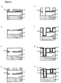
- a first fluorinated dielectric layer (2) is formed on a flattened substrate, i.e. a silicon wafer (1).
- This fluorinated dielectric can be a polymer like or ceramic like dielectric, e.g. a fluorinated silicon oxide.
- this fluorinated dielectric can also be a dielectric where the fluorine is introduced only after the deposition, for instance by plasma fluorination.
- organic polymers comprising Phenyl groups. Examples of such polymers are the benzocyclobutarenes, i.e. benzocyclobutene (BCB) commercially available as Cyclotene 5021TM, poly arylene ether, i.e FLARETM II, aromatic hydrocarbon, i.e. SILKTM, polyimides.
- BCB benzocyclobutarenes
- Cyclotene 5021TM poly arylene ether
- aromatic hydrocarbon i.e. SILKTM
- polyimides polyimides.
- a hard mask layer (3) e.g. a silicon nitride layer, is formed on the first fluorinated dielectric layer.
- a hard mask layer is defined as a layer which can be etched selective to the underlying dielectric layer.
- a lithographic resist layer (4) is deposited and patterned (step a)). The hard mask layer is patterned (step b)) with a RIE (reactive ion etch) step using the patterned lithographic developed resist (4) as a mask thereby creating at least one hole where the surface of the first fluorinated dielectric layer is exposed. After the RIE step the resist leftover is removed.
- a second fluorinated dielectric layer (5) is formed (step c)) over the patterned hard mask layer and a resist layer (6) is formed on this second fluorinated dielectric layer.
- the resist layer is patterned (step d)) and the second fluorinated dielectric layer is etched using the patterned resist layer as a mask which can result in the formation of a trench.
- the hard mask layer functions as an etch stop layer thereby preventing the extension from the trench in the first fluorinated dielectric layer (step e)) .
- the first dielectric layer is then etched using the patterned hard mask layer as a mask to form a contact to the substrate, i.e. exposing the surface of the substrate (step e)).
- the etching of the first and second dielectric layer can be performed using a single etch step or two etch steps.
- the patterned resist layer is removed.
- a near noble metal preferably Co
- a cobalt-fluoride layer at the interface between said dielectric layer and said Co layer to thereby form a barrier for said fluorine.
- This reaction can be stimulated by a heating step.
- the growth of the cobalt-fluoride layer is a self-limiting process yielding a maximum thickness of 5 nm.
- a fluorinated cobaltsilicide is formed with a low contact resistance. So as explained before, in fact a contact barrier layer is formed.
- a conductive layer (8) preferably a Cu layer, is deposited.
- the Cu layer fills the contact in the first and second dielectric layer and the trench in the second dielectric layer.
- the conductive layer is planarized (step g)) to electrically isolate the trenches or contacts one from another.
- This planarization can be performed using chemical mechanical polishing (CMP).
- CMP chemical mechanical polishing
- a second layer of Co (9) can be deposited selectively (step h)) on the Cu. Subsequent deposition of a third fluorinated dielectric (or exposure to fluorine) will lead to a similar formation of a cobalt-fluoride layer on said second Co layer and completely encapsulate the Cu.
- Co is typically a metal that allows deposition by electroless plating. If an adequate activation is performed, each metal, i.e. Cu as well as Co, deposition step can be carried out using plating deposition. Consequently the complete metallization sequence as described in the example can be carried out using plating deposition without the need for physical vapour deposition (PVD).
- PVD physical vapour deposition
- a method for fabricating a metallization structure comprising the steps of:
Landscapes
- Internal Circuitry In Semiconductor Integrated Circuit Devices (AREA)
Priority Applications (3)
| Application Number | Priority Date | Filing Date | Title |
|---|---|---|---|
| DE69928146T DE69928146T2 (de) | 1998-01-28 | 1999-01-27 | Metallisierungsstruktur auf einem fluorhaltigen Dielektrikum und Herstellungsverfahren dafür |
| EP99870014A EP0933815B1 (de) | 1998-01-28 | 1999-01-27 | Metallisierungsstruktur auf einem fluorhaltigen Dielektrikum und Herstellungsverfahren dafür |
| JP01993399A JP4375585B2 (ja) | 1998-01-28 | 1999-01-28 | 含フッ素誘電体を用いた金属配線構造及びその製造方法 |
Applications Claiming Priority (2)
| Application Number | Priority Date | Filing Date | Title |
|---|---|---|---|
| US7289598P | 1998-01-28 | 1998-01-28 | |
| US72895P | 1998-01-28 |
Publications (1)
| Publication Number | Publication Date |
|---|---|
| EP0933814A1 true EP0933814A1 (de) | 1999-08-04 |
Family
ID=22110397
Family Applications (1)
| Application Number | Title | Priority Date | Filing Date |
|---|---|---|---|
| EP98870163A Withdrawn EP0933814A1 (de) | 1998-01-28 | 1998-07-23 | Metallisierungsstruktur auf einem fluorhaltigen Dielektrikum und Herstellungsverfahren dafür |
Country Status (2)
| Country | Link |
|---|---|
| US (2) | US6323555B1 (de) |
| EP (1) | EP0933814A1 (de) |
Cited By (2)
| Publication number | Priority date | Publication date | Assignee | Title |
|---|---|---|---|---|
| WO2001047044A3 (en) * | 1999-12-21 | 2001-12-06 | Plastic Logic Ltd | Forming interconnects |
| CN101567422B (zh) * | 2001-12-21 | 2013-10-02 | 造型逻辑有限公司 | 形成电子器件的方法、电子器件和电子开关器件 |
Families Citing this family (30)
| Publication number | Priority date | Publication date | Assignee | Title |
|---|---|---|---|---|
| US6776792B1 (en) | 1997-04-24 | 2004-08-17 | Advanced Cardiovascular Systems Inc. | Coated endovascular stent |
| JP3132557B2 (ja) * | 1998-04-03 | 2001-02-05 | 日本電気株式会社 | 半導体装置の製造方法 |
| US6245662B1 (en) * | 1998-07-23 | 2001-06-12 | Applied Materials, Inc. | Method of producing an interconnect structure for an integrated circuit |
| US6342733B1 (en) * | 1999-07-27 | 2002-01-29 | International Business Machines Corporation | Reduced electromigration and stressed induced migration of Cu wires by surface coating |
| JP2001135631A (ja) * | 1999-11-10 | 2001-05-18 | Matsushita Electronics Industry Corp | 半導体装置及びその製造方法 |
| US6818990B2 (en) * | 2000-04-03 | 2004-11-16 | Rensselaer Polytechnic Institute | Fluorine diffusion barriers for fluorinated dielectrics in integrated circuits |
| US6531777B1 (en) * | 2000-06-22 | 2003-03-11 | Advanced Micro Devices, Inc. | Barrier metal integrity testing using a dual level line to line leakage testing pattern and partial CMP |
| US6783793B1 (en) | 2000-10-26 | 2004-08-31 | Advanced Cardiovascular Systems, Inc. | Selective coating of medical devices |
| US6565659B1 (en) | 2001-06-28 | 2003-05-20 | Advanced Cardiovascular Systems, Inc. | Stent mounting assembly and a method of using the same to coat a stent |
| US6869818B2 (en) * | 2002-11-18 | 2005-03-22 | Redwood Microsystems, Inc. | Method for producing and testing a corrosion-resistant channel in a silicon device |
| US20040229453A1 (en) * | 2003-05-15 | 2004-11-18 | Jsr Micro, Inc. | Methods of pore sealing and metal encapsulation in porous low k interconnect |
| TW200503163A (en) * | 2003-07-11 | 2005-01-16 | Nanya Technology Corp | Bit line contact structure and manufacturing method thereof |
| JP4413556B2 (ja) * | 2003-08-15 | 2010-02-10 | 東京エレクトロン株式会社 | 成膜方法、半導体装置の製造方法 |
| US7198675B2 (en) | 2003-09-30 | 2007-04-03 | Advanced Cardiovascular Systems | Stent mandrel fixture and method for selectively coating surfaces of a stent |
| US7563324B1 (en) | 2003-12-29 | 2009-07-21 | Advanced Cardiovascular Systems Inc. | System and method for coating an implantable medical device |
| JP2005244031A (ja) * | 2004-02-27 | 2005-09-08 | Nec Electronics Corp | 半導体装置およびその製造方法 |
| US7553377B1 (en) | 2004-04-27 | 2009-06-30 | Advanced Cardiovascular Systems, Inc. | Apparatus and method for electrostatic coating of an abluminal stent surface |
| US7233071B2 (en) * | 2004-10-04 | 2007-06-19 | International Business Machines Corporation | Low-k dielectric layer based upon carbon nanostructures |
| US7632307B2 (en) | 2004-12-16 | 2009-12-15 | Advanced Cardiovascular Systems, Inc. | Abluminal, multilayer coating constructs for drug-delivery stents |
| US8193642B2 (en) * | 2005-06-20 | 2012-06-05 | Tohoku University | Interlayer insulating film, interconnection structure, and methods of manufacturing the same |
| US7867547B2 (en) | 2005-12-19 | 2011-01-11 | Advanced Cardiovascular Systems, Inc. | Selectively coating luminal surfaces of stents |
| US8003156B2 (en) | 2006-05-04 | 2011-08-23 | Advanced Cardiovascular Systems, Inc. | Rotatable support elements for stents |
| US8603530B2 (en) | 2006-06-14 | 2013-12-10 | Abbott Cardiovascular Systems Inc. | Nanoshell therapy |
| US8048448B2 (en) | 2006-06-15 | 2011-11-01 | Abbott Cardiovascular Systems Inc. | Nanoshells for drug delivery |
| US8017237B2 (en) | 2006-06-23 | 2011-09-13 | Abbott Cardiovascular Systems, Inc. | Nanoshells on polymers |
| WO2008039845A2 (en) | 2006-09-26 | 2008-04-03 | Applied Materials, Inc. | Fluorine plasma treatment of high-k gate stack for defect passivation |
| US8048441B2 (en) | 2007-06-25 | 2011-11-01 | Abbott Cardiovascular Systems, Inc. | Nanobead releasing medical devices |
| KR101398634B1 (ko) * | 2008-07-11 | 2014-05-22 | 삼성전자주식회사 | 배선 구조체 및 이를 채택하는 전자 소자 |
| US20100244252A1 (en) * | 2009-03-31 | 2010-09-30 | Jezewski Christopher J | Self Forming Metal Fluoride Barriers for Fluorinated Low-K Dielectrics |
| US20110081500A1 (en) * | 2009-10-06 | 2011-04-07 | Tokyo Electron Limited | Method of providing stable and adhesive interface between fluorine-based low-k material and metal barrier layer |
Citations (4)
| Publication number | Priority date | Publication date | Assignee | Title |
|---|---|---|---|---|
| US5661334A (en) * | 1996-01-16 | 1997-08-26 | Micron Technology, Inc. | Inter-metal dielectric structure which combines fluorine-doped glass and barrier layers |
| JPH09275138A (ja) * | 1996-04-03 | 1997-10-21 | Toshiba Corp | 半導体装置およびその製造方法 |
| EP0849796A2 (de) * | 1996-12-17 | 1998-06-24 | Texas Instruments Incorporated | Verbesserungen in oder in Beziehung zu integrierten Schaltungen |
| GB2323968A (en) * | 1997-04-02 | 1998-10-07 | Nec Corp | Semiconductor device |
Family Cites Families (5)
| Publication number | Priority date | Publication date | Assignee | Title |
|---|---|---|---|---|
| US5753975A (en) * | 1994-09-01 | 1998-05-19 | Kabushiki Kaisha Toshiba | Semiconductor device with improved adhesion between titanium-based metal wiring layer and insulation film |
| US6100184A (en) * | 1997-08-20 | 2000-08-08 | Sematech, Inc. | Method of making a dual damascene interconnect structure using low dielectric constant material for an inter-level dielectric layer |
| JP3287392B2 (ja) * | 1997-08-22 | 2002-06-04 | 日本電気株式会社 | 半導体装置およびその製造方法 |
| US6265779B1 (en) * | 1998-08-11 | 2001-07-24 | International Business Machines Corporation | Method and material for integration of fuorine-containing low-k dielectrics |
| US6144099A (en) * | 1999-03-30 | 2000-11-07 | Advanced Micro Devices, Inc. | Semiconductor metalization barrier |
-
1998
- 1998-07-23 EP EP98870163A patent/EP0933814A1/de not_active Withdrawn
-
1999
- 1999-01-27 US US09/237,876 patent/US6323555B1/en not_active Expired - Fee Related
-
2001
- 2001-08-13 US US09/928,912 patent/US6635964B2/en not_active Expired - Lifetime
Patent Citations (5)
| Publication number | Priority date | Publication date | Assignee | Title |
|---|---|---|---|---|
| US5661334A (en) * | 1996-01-16 | 1997-08-26 | Micron Technology, Inc. | Inter-metal dielectric structure which combines fluorine-doped glass and barrier layers |
| JPH09275138A (ja) * | 1996-04-03 | 1997-10-21 | Toshiba Corp | 半導体装置およびその製造方法 |
| US5850102A (en) * | 1996-04-03 | 1998-12-15 | Kabushiki Kaisha Toshiba | Semiconductor device having a second insulating layer which includes carbon or fluorine at a density lower than a first insulating layer |
| EP0849796A2 (de) * | 1996-12-17 | 1998-06-24 | Texas Instruments Incorporated | Verbesserungen in oder in Beziehung zu integrierten Schaltungen |
| GB2323968A (en) * | 1997-04-02 | 1998-10-07 | Nec Corp | Semiconductor device |
Non-Patent Citations (2)
| Title |
|---|
| LI WEIDAN ET AL: "Thermal stability study of the interconnect system with fluorinated silicate glass as IMD layers", 1997, PROCEEDINGS OF THE 1997 MRS SPRING MEETING;SAN FRANCISCO, CA, USA APR 1-4 1997, MATER RES SOC SYMP PROC;MATERIALS RESEARCH SOCIETY SYMPOSIUM PROCEEDINGS; LOW-DIELECTRIC CONSTANT MATERIALS III 1997 MRS, WARRENDALE, PA, USA, PAGE(S) 261 - 266, XP002102302 * |
| PATENT ABSTRACTS OF JAPAN vol. 098, no. 002 30 January 1998 (1998-01-30) * |
Cited By (4)
| Publication number | Priority date | Publication date | Assignee | Title |
|---|---|---|---|---|
| WO2001047044A3 (en) * | 1999-12-21 | 2001-12-06 | Plastic Logic Ltd | Forming interconnects |
| US7098061B2 (en) | 1999-12-21 | 2006-08-29 | Plastic Logic Limited | Forming interconnects using locally deposited solvents |
| US7763501B2 (en) | 1999-12-21 | 2010-07-27 | Plastic Logic Limited | Forming interconnects |
| CN101567422B (zh) * | 2001-12-21 | 2013-10-02 | 造型逻辑有限公司 | 形成电子器件的方法、电子器件和电子开关器件 |
Also Published As
| Publication number | Publication date |
|---|---|
| US20020066957A1 (en) | 2002-06-06 |
| US6323555B1 (en) | 2001-11-27 |
| US6635964B2 (en) | 2003-10-21 |
Similar Documents
| Publication | Publication Date | Title |
|---|---|---|
| EP0933814A1 (de) | Metallisierungsstruktur auf einem fluorhaltigen Dielektrikum und Herstellungsverfahren dafür | |
| US6509258B2 (en) | Etch stop in damascene interconnect structure and method of making | |
| KR101606178B1 (ko) | 반도체 구조물 형성 방법 | |
| US20020089063A1 (en) | Copper dual damascene interconnect technology | |
| US20040219783A1 (en) | Copper dual damascene interconnect technology | |
| US6573572B2 (en) | Damascene structure and method of making | |
| US20020167089A1 (en) | Copper dual damascene interconnect technology | |
| US8119519B2 (en) | Semiconductor device manufacturing method | |
| US6130157A (en) | Method to form an encapsulation layer over copper interconnects | |
| WO2002061823A1 (en) | Integration of organic fill for dual damascene process | |
| US7285853B2 (en) | Multilayer anti-reflective coating for semiconductor lithography and the method for forming the same | |
| US6713382B1 (en) | Vapor treatment for repairing damage of low-k dielectric | |
| US6503835B1 (en) | Method of making an organic copper diffusion barrier layer | |
| US6576545B1 (en) | Semiconductor devices with dual nature capping/ARC layers on fluorine doped silica glass inter-layer dielectrics and method of forming capping/ARC layers | |
| KR100614782B1 (ko) | 이중 다마신 구조를 포함하는 집적회로 제조방법 및 집적회로 | |
| US7247565B2 (en) | Methods for fabricating a copper interconnect | |
| US6713874B1 (en) | Semiconductor devices with dual nature capping/arc layers on organic-doped silica glass inter-layer dielectrics | |
| US20060118955A1 (en) | Robust copper interconnection structure and fabrication method thereof | |
| US20030219968A1 (en) | Sacrificial inlay process for improved integration of porous interlevel dielectrics | |
| US6448654B1 (en) | Ultra thin etch stop layer for damascene process | |
| US20020127849A1 (en) | Method of manufacturing dual damascene structure | |
| US6495447B1 (en) | Use of hydrogen doping for protection of low-k dielectric layers | |
| US6927160B1 (en) | Fabrication of copper-containing region such as electrical interconnect | |
| US7132306B1 (en) | Method of forming an interlevel dielectric layer employing dielectric etch-back process without extra mask set | |
| EP0933815B1 (de) | Metallisierungsstruktur auf einem fluorhaltigen Dielektrikum und Herstellungsverfahren dafür |
Legal Events
| Date | Code | Title | Description |
|---|---|---|---|
| PUAI | Public reference made under article 153(3) epc to a published international application that has entered the european phase |
Free format text: ORIGINAL CODE: 0009012 |
|
| AK | Designated contracting states |
Kind code of ref document: A1 Designated state(s): AT BE CH CY DE DK ES FI FR GB GR IE IT LI LU MC NL PT SE |
|
| AX | Request for extension of the european patent |
Free format text: AL;LT;LV;MK;RO;SI |
|
| AKX | Designation fees paid | ||
| REG | Reference to a national code |
Ref country code: DE Ref legal event code: 8566 |
|
| STAA | Information on the status of an ep patent application or granted ep patent |
Free format text: STATUS: THE APPLICATION IS DEEMED TO BE WITHDRAWN |
|
| 18D | Application deemed to be withdrawn |
Effective date: 20000208 |