EP0933866A2 - Dispositif d'alimentation de puissance à découpage - Google Patents
Dispositif d'alimentation de puissance à découpage Download PDFInfo
- Publication number
- EP0933866A2 EP0933866A2 EP99101859A EP99101859A EP0933866A2 EP 0933866 A2 EP0933866 A2 EP 0933866A2 EP 99101859 A EP99101859 A EP 99101859A EP 99101859 A EP99101859 A EP 99101859A EP 0933866 A2 EP0933866 A2 EP 0933866A2
- Authority
- EP
- European Patent Office
- Prior art keywords
- voltage
- switching
- winding
- switching element
- circuit
- Prior art date
- Legal status (The legal status is an assumption and is not a legal conclusion. Google has not performed a legal analysis and makes no representation as to the accuracy of the status listed.)
- Granted
Links
- 238000004804 winding Methods 0.000 claims abstract description 120
- 230000000670 limiting effect Effects 0.000 claims abstract description 17
- 230000002441 reversible effect Effects 0.000 claims abstract description 17
- 239000003990 capacitor Substances 0.000 claims description 40
- 238000000034 method Methods 0.000 claims 4
- 238000007599 discharging Methods 0.000 claims 2
- 230000002829 reductive effect Effects 0.000 description 10
- 238000010586 diagram Methods 0.000 description 2
- 238000009499 grossing Methods 0.000 description 2
- 230000036962 time dependent Effects 0.000 description 2
- 230000003247 decreasing effect Effects 0.000 description 1
- 230000003111 delayed effect Effects 0.000 description 1
- 230000010355 oscillation Effects 0.000 description 1
- 230000002035 prolonged effect Effects 0.000 description 1
- 230000000630 rising effect Effects 0.000 description 1
- 230000006641 stabilisation Effects 0.000 description 1
- 238000011105 stabilization Methods 0.000 description 1
Images



Classifications
-
- H—ELECTRICITY
- H02—GENERATION; CONVERSION OR DISTRIBUTION OF ELECTRIC POWER
- H02M—APPARATUS FOR CONVERSION BETWEEN AC AND AC, BETWEEN AC AND DC, OR BETWEEN DC AND DC, AND FOR USE WITH MAINS OR SIMILAR POWER SUPPLY SYSTEMS; CONVERSION OF DC OR AC INPUT POWER INTO SURGE OUTPUT POWER; CONTROL OR REGULATION THEREOF
- H02M3/00—Conversion of DC power input into DC power output
- H02M3/22—Conversion of DC power input into DC power output with intermediate conversion into AC
- H02M3/24—Conversion of DC power input into DC power output with intermediate conversion into AC by static converters
- H02M3/28—Conversion of DC power input into DC power output with intermediate conversion into AC by static converters using discharge tubes with control electrode or semiconductor devices with control electrode to produce the intermediate AC
- H02M3/325—Conversion of DC power input into DC power output with intermediate conversion into AC by static converters using discharge tubes with control electrode or semiconductor devices with control electrode to produce the intermediate AC using devices of a triode or a transistor type requiring continuous application of a control signal
- H02M3/335—Conversion of DC power input into DC power output with intermediate conversion into AC by static converters using discharge tubes with control electrode or semiconductor devices with control electrode to produce the intermediate AC using devices of a triode or a transistor type requiring continuous application of a control signal using semiconductor devices only
- H02M3/338—Conversion of DC power input into DC power output with intermediate conversion into AC by static converters using discharge tubes with control electrode or semiconductor devices with control electrode to produce the intermediate AC using devices of a triode or a transistor type requiring continuous application of a control signal using semiconductor devices only in a self-oscillating arrangement
- H02M3/3385—Conversion of DC power input into DC power output with intermediate conversion into AC by static converters using discharge tubes with control electrode or semiconductor devices with control electrode to produce the intermediate AC using devices of a triode or a transistor type requiring continuous application of a control signal using semiconductor devices only in a self-oscillating arrangement with automatic control of output voltage or current
-
- H—ELECTRICITY
- H02—GENERATION; CONVERSION OR DISTRIBUTION OF ELECTRIC POWER
- H02M—APPARATUS FOR CONVERSION BETWEEN AC AND AC, BETWEEN AC AND DC, OR BETWEEN DC AND DC, AND FOR USE WITH MAINS OR SIMILAR POWER SUPPLY SYSTEMS; CONVERSION OF DC OR AC INPUT POWER INTO SURGE OUTPUT POWER; CONTROL OR REGULATION THEREOF
- H02M1/00—Details of apparatus for conversion
- H02M1/0003—Details of control, feedback or regulation circuits
- H02M1/0032—Control circuits allowing low power mode operation, e.g. in standby mode
-
- Y—GENERAL TAGGING OF NEW TECHNOLOGICAL DEVELOPMENTS; GENERAL TAGGING OF CROSS-SECTIONAL TECHNOLOGIES SPANNING OVER SEVERAL SECTIONS OF THE IPC; TECHNICAL SUBJECTS COVERED BY FORMER USPC CROSS-REFERENCE ART COLLECTIONS [XRACs] AND DIGESTS
- Y02—TECHNOLOGIES OR APPLICATIONS FOR MITIGATION OR ADAPTATION AGAINST CLIMATE CHANGE
- Y02B—CLIMATE CHANGE MITIGATION TECHNOLOGIES RELATED TO BUILDINGS, e.g. HOUSING, HOUSE APPLIANCES OR RELATED END-USER APPLICATIONS
- Y02B70/00—Technologies for an efficient end-user side electric power management and consumption
- Y02B70/10—Technologies improving the efficiency by using switched-mode power supplies [SMPS], i.e. efficient power electronics conversion e.g. power factor correction or reduction of losses in power supplies or efficient standby modes
Definitions
- a voltage detecting circuit 4 provided on the output side of the DC-DC converter circuit 3 is made up of a resistor R2, a light emitting diode PD1 on the light emitting side of a photocoupler PC1, a shunt regulator Sr and resistors R3, R4.
- the resistor R2, the shunt regulator Sr, and the resistors R3, R4 are connected in series with one another, and provided in parallel to the capacitor C2 of the DC-DC converter circuit 3.
- the resistors R3, R4 are connected in series with each other, and provided in parallel to the capacitor C2.
- a connection of the resistors R3, R4 is connected to the shunt regulator Sr.
- the capacitor C4 since a voltage reverse in polarity is applied to the capacitor C4, the capacitor C4, after it is discharged, is charged in the reverse direction, and the base emitter voltage Vbe of the transistor Q2 is negatively biased, resulting in the turn-off of the transistor Q2.
- the transistor Q2 turns on only at the instant that it triggers the turn off of FET Q1.
- a current flowing in the phototransistor PT1 of the photocoupler PC1 is increased.
- the current flowing in the phototransistor PT1 together with the current flowing in the resistor R6 when the voltage Vb generated in the feedback winding Nb is positive in polarity as described above, acts to charge the capacitor C4. Accordingly, when the current flowing in the phototransistor PT1 is increased, the time taken to charge the capacitor C4 is shortened. As a result, the time taken until the transistor Q2 is turned on is shortened, and also the time until FET Q1 is turned off, that is, the time while the FET Q1 is on, is shortened.
- a switching power supply device comprises a transformer having a primary winding, a secondary winding, and a feedback winding, a switching element connected in series with the primary winding, a controlling element connected to a control terminal of the switching element, a controlling circuit provided between the controlling element and the feedback winding, and a rectifying circuit connected to the secondary winding, and further comprising a frequency limiting circuit including a charging circuit adapted to be charged at a voltage reverse in polarity, produced in said feedback winding, and a kick voltage absorbing circuit for absorbing a current developed at a kick voltage in said feedback winding, by discharge of said charging circuit, whereby the switching frequency is reduced by prolongation of the off-state time-period of said switching element in correspondence to a light load signal when the load is light.
- the frequency limiting circuit is made to operate in correspondence to a light load signal from an equipment when the load is light.
- the switching element is prevented from being turned on, which will be caused by the kick voltage produced in the feedback winding, and the switching frequency is reduced, so that the switching loss can be reduced.
- the efficiency of the switching power supply device is improved.
- FIG. 1 is a circuit diagram showing a switching power supply device according to an embodiment of the present invention.
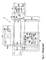
- FIG. 4 is a circuit diagram showing a conventional switching power supply device.
- the voltage Nb produced in the feedback winding Nb is changed to a voltage oscillating from the reverse polarity, on the base line of 0V.
- the voltage is in the opposite direction to the diode D4 so that the current ceases to flow.
- the electric charge stored in the capacitor C6 is discharged through the phototransistor PT2, the resistor R12, and the resistor R11 of the kick voltage absorbing circuit (state B).
- the base emitter voltage of the transistor Q3 exceeds a threshold so that the transistor Q3 is turned on.
- FET Q1 which is prevented from being turned on by the kick voltage generated in the feedback winding Nb, is turned on in the same manner as in the starting-up. Since the resistance of the starting-up resistors R1 is set to a high value, the timing of the turn-on of the FET Q1 is delayed. Accordingly, the switching frequency can be reduced.
Landscapes
- Engineering & Computer Science (AREA)
- Power Engineering (AREA)
- Dc-Dc Converters (AREA)
Applications Claiming Priority (2)
| Application Number | Priority Date | Filing Date | Title |
|---|---|---|---|
| JP01613998A JP3273598B2 (ja) | 1998-01-28 | 1998-01-28 | スイッチング電源装置 |
| JP1613998 | 1998-01-28 |
Publications (3)
| Publication Number | Publication Date |
|---|---|
| EP0933866A2 true EP0933866A2 (fr) | 1999-08-04 |
| EP0933866A3 EP0933866A3 (fr) | 2000-02-23 |
| EP0933866B1 EP0933866B1 (fr) | 2009-12-09 |
Family
ID=11908178
Family Applications (1)
| Application Number | Title | Priority Date | Filing Date |
|---|---|---|---|
| EP99101859A Expired - Lifetime EP0933866B1 (fr) | 1998-01-28 | 1999-01-28 | Dispositif d'alimentation électrique à découpage |
Country Status (4)
| Country | Link |
|---|---|
| US (1) | US6185112B1 (fr) |
| EP (1) | EP0933866B1 (fr) |
| JP (1) | JP3273598B2 (fr) |
| DE (1) | DE69941748D1 (fr) |
Cited By (4)
| Publication number | Priority date | Publication date | Assignee | Title |
|---|---|---|---|---|
| GB2370887A (en) * | 2000-09-06 | 2002-07-10 | Murata Manufacturing Co | Ringing choke converter switching power supply unit |
| GB2374214A (en) * | 2000-12-28 | 2002-10-09 | Murata Manufacturing Co | Switching power supply unit |
| US6829816B2 (en) | 2001-01-25 | 2004-12-14 | Murata Manufacturing Co., Ltd. | Method of manufacturing nonreciprocal circuit device |
| CN110620514A (zh) * | 2018-06-20 | 2019-12-27 | 虹冠电子工业股份有限公司 | 在开关功率转换器中的同步整流的系统和方法 |
Families Citing this family (6)
| Publication number | Priority date | Publication date | Assignee | Title |
|---|---|---|---|---|
| DE69911671T2 (de) | 1998-02-24 | 2004-09-30 | Sharp K.K. | Schaltnetzteil |
| JP3470693B2 (ja) | 2000-10-25 | 2003-11-25 | 株式会社村田製作所 | 自励発振型スイッチング電源装置 |
| TW587362B (en) * | 2000-11-10 | 2004-05-11 | Delta Electronics Inc | Light-load detection method and detection circuit of switching type power source system |
| DE50301019D1 (de) * | 2003-07-15 | 2005-09-22 | Friwo Mobile Power Gmbh | Freischwingender Sperrwandler mit Strom- und Spannungsbegrenzung |
| JP5683241B2 (ja) * | 2010-12-06 | 2015-03-11 | キヤノン株式会社 | スイッチング電源装置及び画像形成装置 |
| US12294307B2 (en) * | 2021-08-27 | 2025-05-06 | Na Vitas Semiconductor Limited | System and methods for reducing auxiliary transformer winding turns |
Family Cites Families (12)
| Publication number | Priority date | Publication date | Assignee | Title |
|---|---|---|---|---|
| US4283759A (en) * | 1977-08-01 | 1981-08-11 | Toko, Inc. | Switching regulator |
| JPS62166777A (ja) * | 1986-01-16 | 1987-07-23 | Sanken Electric Co Ltd | 直流−直流変換器 |
| US4758937A (en) * | 1986-01-16 | 1988-07-19 | Sanken Electric Company, Ltd. | DC-DC converter |
| JPS62166776A (ja) | 1986-01-16 | 1987-07-23 | Sanken Electric Co Ltd | 直流−直流変換器 |
| JPS63138881U (fr) * | 1987-02-27 | 1988-09-13 | ||
| JP2773195B2 (ja) * | 1988-04-05 | 1998-07-09 | 松下電器産業株式会社 | スイッチング電源装置 |
| JP3087618B2 (ja) * | 1995-07-27 | 2000-09-11 | 株式会社村田製作所 | スイッチング電源 |
| JP3367300B2 (ja) * | 1995-09-18 | 2003-01-14 | ヤマハ株式会社 | スイッチング電源回路 |
| JP2845188B2 (ja) * | 1995-12-11 | 1999-01-13 | サンケン電気株式会社 | Dc−dcコンバ−タ |
| JPH1155949A (ja) * | 1997-06-06 | 1999-02-26 | Canon Inc | 電源装置 |
| US5812383A (en) * | 1997-07-31 | 1998-09-22 | Philips Electronics North North America Corporation | Low power stand-by for switched-mode power supply circuit with burst mode operation |
| US5852550A (en) * | 1997-08-04 | 1998-12-22 | Philips Electronics North America Corporation | Switched-mode power supply circuit having a very low power stand-by mode |
-
1998
- 1998-01-28 JP JP01613998A patent/JP3273598B2/ja not_active Expired - Fee Related
-
1999
- 1999-01-19 US US09/232,786 patent/US6185112B1/en not_active Expired - Fee Related
- 1999-01-28 DE DE69941748T patent/DE69941748D1/de not_active Expired - Fee Related
- 1999-01-28 EP EP99101859A patent/EP0933866B1/fr not_active Expired - Lifetime
Cited By (7)
| Publication number | Priority date | Publication date | Assignee | Title |
|---|---|---|---|---|
| GB2370887A (en) * | 2000-09-06 | 2002-07-10 | Murata Manufacturing Co | Ringing choke converter switching power supply unit |
| US6529392B2 (en) | 2000-09-06 | 2003-03-04 | Murata Manufacturing Co., Ltd. | Switching power supply unit |
| GB2370887B (en) * | 2000-09-06 | 2003-04-16 | Murata Manufacturing Co | Switching power supply unit |
| GB2374214A (en) * | 2000-12-28 | 2002-10-09 | Murata Manufacturing Co | Switching power supply unit |
| GB2374214B (en) * | 2000-12-28 | 2004-10-20 | Murata Manufacturing Co | Switching power supply unit |
| US6829816B2 (en) | 2001-01-25 | 2004-12-14 | Murata Manufacturing Co., Ltd. | Method of manufacturing nonreciprocal circuit device |
| CN110620514A (zh) * | 2018-06-20 | 2019-12-27 | 虹冠电子工业股份有限公司 | 在开关功率转换器中的同步整流的系统和方法 |
Also Published As
| Publication number | Publication date |
|---|---|
| US6185112B1 (en) | 2001-02-06 |
| JP3273598B2 (ja) | 2002-04-08 |
| JPH11215827A (ja) | 1999-08-06 |
| DE69941748D1 (de) | 2010-01-21 |
| EP0933866B1 (fr) | 2009-12-09 |
| EP0933866A3 (fr) | 2000-02-23 |
Similar Documents
| Publication | Publication Date | Title |
|---|---|---|
| US6788556B2 (en) | Switching power source device | |
| CN100392972C (zh) | 具有过流保护的开关模式电源 | |
| KR100422764B1 (ko) | 스위칭 전원 장치 | |
| US6038143A (en) | Self-oscillation type switching power supply having time constant circuit electronic switch an external voltage and having charging time variable in response to output voltage | |
| EP0935332A2 (fr) | Dispositif d'alimentation de puissance à découpage auto-oscillant | |
| US6198637B1 (en) | Switching power supply circuit | |
| US6525948B2 (en) | Apparatus and method for the detection of circuit irregularities and for circuit protection of a power supply | |
| EP0933866B1 (fr) | Dispositif d'alimentation électrique à découpage | |
| US6532159B2 (en) | Switching power supply unit | |
| US20080007976A1 (en) | Power supply device and electric appliance provided therewith | |
| US6072702A (en) | Ringing choke converter | |
| US5841642A (en) | Tuned switch-mode power supply with current mode control | |
| JP3527636B2 (ja) | 自励型dc−dcコンバータ | |
| US6081433A (en) | Switching power supply apparatus | |
| US6483725B2 (en) | DC/DC conversion circuit having a switching frequency proportional to power output | |
| JP3613731B2 (ja) | 無負荷時省電力電源装置 | |
| JP4329113B2 (ja) | スイッチング電源装置 | |
| KR20020070144A (ko) | 스위칭 모드 파워 서플라이 | |
| JP2737391B2 (ja) | リンギングチョークコンバータ | |
| JP3641351B2 (ja) | リンギングチョークコンバータ | |
| JPH05344721A (ja) | スイッチングレギュレ−タ | |
| JPS61177163A (ja) | ソフト・スタ−ト方式 | |
| JPH07106064B2 (ja) | Dc−dcコンバータ | |
| KR920003089Y1 (ko) | 링잉 초크 콘버터 방식의 스위칭 전원 장치 | |
| JPH06189545A (ja) | スイッチング電源装置 |
Legal Events
| Date | Code | Title | Description |
|---|---|---|---|
| PUAI | Public reference made under article 153(3) epc to a published international application that has entered the european phase |
Free format text: ORIGINAL CODE: 0009012 |
|
| 17P | Request for examination filed |
Effective date: 19990128 |
|
| AK | Designated contracting states |
Kind code of ref document: A2 Designated state(s): CH DE FR GB LI |
|
| AX | Request for extension of the european patent |
Free format text: AL;LT;LV;MK;RO;SI |
|
| PUAL | Search report despatched |
Free format text: ORIGINAL CODE: 0009013 |
|
| AK | Designated contracting states |
Kind code of ref document: A3 Designated state(s): AT BE CH CY DE DK ES FI FR GB GR IE IT LI LU MC NL PT SE |
|
| AX | Request for extension of the european patent |
Free format text: AL;LT;LV;MK;RO;SI |
|
| AKX | Designation fees paid |
Free format text: CH DE FR GB LI |
|
| RAP1 | Party data changed (applicant data changed or rights of an application transferred) |
Owner name: MURATA MANUFACTURING CO., LTD. |
|
| 17Q | First examination report despatched |
Effective date: 20071115 |
|
| GRAP | Despatch of communication of intention to grant a patent |
Free format text: ORIGINAL CODE: EPIDOSNIGR1 |
|
| GRAS | Grant fee paid |
Free format text: ORIGINAL CODE: EPIDOSNIGR3 |
|
| GRAA | (expected) grant |
Free format text: ORIGINAL CODE: 0009210 |
|
| AK | Designated contracting states |
Kind code of ref document: B1 Designated state(s): CH DE FR GB LI |
|
| REG | Reference to a national code |
Ref country code: GB Ref legal event code: FG4D |
|
| REG | Reference to a national code |
Ref country code: CH Ref legal event code: EP |
|
| REF | Corresponds to: |
Ref document number: 69941748 Country of ref document: DE Date of ref document: 20100121 Kind code of ref document: P |
|
| PGFP | Annual fee paid to national office [announced via postgrant information from national office to epo] |
Ref country code: GB Payment date: 20100121 Year of fee payment: 12 |
|
| REG | Reference to a national code |
Ref country code: CH Ref legal event code: PL |
|
| PLBE | No opposition filed within time limit |
Free format text: ORIGINAL CODE: 0009261 |
|
| STAA | Information on the status of an ep patent application or granted ep patent |
Free format text: STATUS: NO OPPOSITION FILED WITHIN TIME LIMIT |
|
| REG | Reference to a national code |
Ref country code: FR Ref legal event code: ST Effective date: 20100930 |
|
| PG25 | Lapsed in a contracting state [announced via postgrant information from national office to epo] |
Ref country code: LI Free format text: LAPSE BECAUSE OF NON-PAYMENT OF DUE FEES Effective date: 20100131 Ref country code: FR Free format text: LAPSE BECAUSE OF NON-PAYMENT OF DUE FEES Effective date: 20100209 Ref country code: CH Free format text: LAPSE BECAUSE OF NON-PAYMENT OF DUE FEES Effective date: 20100131 |
|
| 26N | No opposition filed |
Effective date: 20100910 |
|
| PG25 | Lapsed in a contracting state [announced via postgrant information from national office to epo] |
Ref country code: DE Free format text: LAPSE BECAUSE OF NON-PAYMENT OF DUE FEES Effective date: 20100803 |
|
| GBPC | Gb: european patent ceased through non-payment of renewal fee |
Effective date: 20110128 |
|
| PG25 | Lapsed in a contracting state [announced via postgrant information from national office to epo] |
Ref country code: GB Free format text: LAPSE BECAUSE OF NON-PAYMENT OF DUE FEES Effective date: 20110128 |