EP0935131A2 - Oberflächenplasmonenresonanz-Sensor mit wellenlängenstabilisierter Laserlichtquelle - Google Patents
Oberflächenplasmonenresonanz-Sensor mit wellenlängenstabilisierter Laserlichtquelle Download PDFInfo
- Publication number
- EP0935131A2 EP0935131A2 EP99102150A EP99102150A EP0935131A2 EP 0935131 A2 EP0935131 A2 EP 0935131A2 EP 99102150 A EP99102150 A EP 99102150A EP 99102150 A EP99102150 A EP 99102150A EP 0935131 A2 EP0935131 A2 EP 0935131A2
- Authority
- EP
- European Patent Office
- Prior art keywords
- laser
- semiconductor laser
- surface plasmon
- dielectric block
- laser beam
- Prior art date
- Legal status (The legal status is an assumption and is not a legal conclusion. Google has not performed a legal analysis and makes no representation as to the accuracy of the status listed.)
- Ceased
Links
- 238000002198 surface plasmon resonance spectroscopy Methods 0.000 title 1
- 230000003287 optical effect Effects 0.000 claims abstract description 54
- 230000010355 oscillation Effects 0.000 claims abstract description 50
- 230000000087 stabilizing effect Effects 0.000 claims abstract description 33
- 239000002184 metal Substances 0.000 claims abstract description 28
- 229910052751 metal Inorganic materials 0.000 claims abstract description 28
- 239000004065 semiconductor Substances 0.000 claims description 86
- 239000000835 fiber Substances 0.000 claims description 39
- 239000013307 optical fiber Substances 0.000 claims description 2
- 239000000463 material Substances 0.000 description 11
- 238000005259 measurement Methods 0.000 description 7
- 230000003595 spectral effect Effects 0.000 description 4
- 230000006835 compression Effects 0.000 description 2
- 238000007906 compression Methods 0.000 description 2
- 239000012530 fluid Substances 0.000 description 2
- 230000001902 propagating effect Effects 0.000 description 2
- 238000011088 calibration curve Methods 0.000 description 1
- 230000005684 electric field Effects 0.000 description 1
- 239000003574 free electron Substances 0.000 description 1
- YBMRDBCBODYGJE-UHFFFAOYSA-N germanium oxide Inorganic materials O=[Ge]=O YBMRDBCBODYGJE-UHFFFAOYSA-N 0.000 description 1
- 239000011521 glass Substances 0.000 description 1
- PCHJSUWPFVWCPO-UHFFFAOYSA-N gold Chemical compound [Au] PCHJSUWPFVWCPO-UHFFFAOYSA-N 0.000 description 1
- 229910052737 gold Inorganic materials 0.000 description 1
- 239000010931 gold Substances 0.000 description 1
- PVADDRMAFCOOPC-UHFFFAOYSA-N oxogermanium Chemical compound [Ge]=O PVADDRMAFCOOPC-UHFFFAOYSA-N 0.000 description 1
- 230000000704 physical effect Effects 0.000 description 1
- 230000010287 polarization Effects 0.000 description 1
- 229910052709 silver Inorganic materials 0.000 description 1
- 239000004332 silver Substances 0.000 description 1
- 239000000126 substance Substances 0.000 description 1
Images






Classifications
-
- G—PHYSICS
- G01—MEASURING; TESTING
- G01N—INVESTIGATING OR ANALYSING MATERIALS BY DETERMINING THEIR CHEMICAL OR PHYSICAL PROPERTIES
- G01N21/00—Investigating or analysing materials by the use of optical means, i.e. using sub-millimetre waves, infrared, visible or ultraviolet light
- G01N21/17—Systems in which incident light is modified in accordance with the properties of the material investigated
- G01N21/55—Specular reflectivity
- G01N21/552—Attenuated total reflection
- G01N21/553—Attenuated total reflection and using surface plasmons
Definitions
- This invention relates to a surface plasmon sensor for quantitatively analyzing a material in a sample utilizing generation of surface plasmon, and more particularly to a surface plasmon sensor in which the light source is improved to improve accuracy in analysis.
- the plasmon sensor using the Kretschmann configuration basically comprises a dielectric block shaped, for instance, like a prism, a metal film which is formed on one face of the dielectric block and is brought into contact with a sample, a light source emitting a light beam, an optical system which causes the light beam to enter the dielectric block so that the light beam is reflected in total reflection at the interface of the dielectric block and the metal film and various angles of incidence of the light beam to the interface of the dielectric block and the metal film including an angle of incidence at which surface plasmon is generated can be obtained, and a photodetector means which is able to detect the intensity of the light beam reflected in total reflection from the interface for the various angles of incidence.
- a relatively thin incident light beam may be caused to impinge upon the interface while deflecting the incident light beam or a relatively thick incident light beam may be caused to converge on the interface so that components of the incident light beam impinge upon the interface at various angles.
- the light beam which is reflected from the interface at an angle which varies as the incident light beam is deflected may be detected by a photodetector which is moved in synchronization with deflection of the incident light beam or by an area sensor extending in the direction in which reflected light beam is moved as a result of deflection.
- an area sensor which extends in directions so that all the components of light reflected from the interface at various angles can be detected by the area sensor may be used.
- a plasmon sensor when a light beam impinges upon the metal film at a particular angle of incidence ⁇ sp not smaller than the angle of total internal reflection, evanescent waves having an electric field distribution are generated in the sample in contact with the metal film and surface plasmon is excited in the interface between the metal film and the sample.
- the wave vector of the evanescent waves is equal to the wave number of the surface plasmon and wave number matching is established, the evanescent waves and the surface plasmon resonate and light energy is transferred to the surface plasmon, whereby the intensity of light reflected in total reflection from the interface of the dielectric block and the metal film sharply drops.
- Ksp ( ⁇ ) ⁇ c ⁇ m ( ⁇ ) ⁇ s ⁇ m ( ⁇ ) + ⁇ s
- Ksp represents the wave number of the surface plasmon
- ⁇ represents the angular frequency of the surface plasmon
- c represents the speed of light in a vacuum
- ⁇ m and ⁇ s respectively represent the dielectric constants of the metal and the sample.
- the concentration of a specific material in the sample can be determined on the basis of a predetermined calibration curve or the like. Accordingly, a specific component in the sample can be quantitatively analyzed by detecting the angle of incidence ⁇ sp at which the intensity of light reflected in total reflection from the interface of the prism and the metal film sharply drops.
- the primary object of the present invention is to provide a surface plasmon sensor in which a sufficiently high accuracy of measurement can be realized.
- the surface plasmon sensor of the present invention comprises a dielectric block, a metal film, a light source emitting a light beam, an optical system, and a photodetector means which are described above and is characterized in that a laser provided with an oscillation wavelength stabilizing means for stabilizing the wavelength at which the laser oscillates is used as the light source.
- the oscillation wavelength stabilizing means may comprise, for instance, a beam feedback optical system which feeds a part of a laser beam emitted from the semiconductor laser back to the semiconductor laser and a wavelength selector such as a grating or a band pass filter which selects the wavelength of the laser beam to be fed back to the semiconductor laser.
- the beam feedback optical system may comprise a beam splitter means which is disposed on the optical path of the laser beam traveling from the semiconductor laser to the dielectric block and splits a part of the laser beam and a reflective grating which reflects the laser beam split by the beam splitter means to retrace its path, and the reflective grating may double as the wavelength selector.
- the beam feedback optical system and the wavelength selector by a partial reflection type grating which is disposed on the optical path of the laser beam traveling from the semiconductor laser to the dielectric block and reflects a part of the laser beam toward the semiconductor laser.
- the beam feedback optical system and the wavelength selector by a reflective grating which reflects toward the semiconductor laser a rearward laser beam emitted from the semiconductor laser in the direction opposite to the laser beam traveling from the semiconductor laser to the dielectric block.
- the oscillation wavelength stabilizing means may comprise a combination of a beam feedback optical system comprising a beam splitter means which is disposed on the optical path of the laser beam traveling from the semiconductor laser to the dielectric block and splits a part of the laser beam and a mirror which reflects the laser beam split by the beam splitter means to retrace its path and a narrow-band pass filter disposed on the optical path of the laser beam between the mirror and the semiconductor laser.
- a beam feedback optical system comprising a beam splitter means which is disposed on the optical path of the laser beam traveling from the semiconductor laser to the dielectric block and splits a part of the laser beam and a mirror which reflects the laser beam split by the beam splitter means to retrace its path and a narrow-band pass filter disposed on the optical path of the laser beam between the mirror and the semiconductor laser.
- the oscillation wavelength stabilizing means may comprise a combination of a beam feedback optical system comprising a half-silvered mirror which is disposed on the optical path of the laser beam traveling from the semiconductor laser to the dielectric block and reflects a part of the laser beam toward the semiconductor laser and a narrow-band pass filter disposed on the optical path of the laser beam between the half-silvered mirror and the semiconductor laser.
- the oscillation wavelength stabilizing means may comprise a combination of a beam feedback optical system comprising a mirror which reflects toward the semiconductor laser a rearward laser beam emitted from the semiconductor laser in the direction opposite to the laser beam traveling from the semiconductor laser to the dielectric block and a narrow-band pass filter disposed on the optical path of the rearward laser beam between the mirror and the semiconductor laser.
- the wavelength selector may be used a fiber grating comprising an optical fiber which has a plurality of refractive index varying portions formed in the core at regular intervals and reflects and diffracts a laser beam.
- the beam feedback optical system may comprise a beam splitter means which is disposed on the optical path of the laser beam traveling from the semiconductor laser to the dielectric block and splits a part of the laser beam and a fiber grating which reflects the laser beam split by the beam splitter means to retrace its path, and the fiber grating may double as the wavelength selector.
- the beam feedback optical system and the wavelength selector by a partial reflection type fiber grating which is disposed on the optical path of the laser beam traveling from the semiconductor laser to the dielectric block and reflects a part of the laser beam toward the semiconductor laser.
- the beam feedback optical system and the wavelength selector by a fiber grating which reflects toward the semiconductor laser a rearward laser beam emitted from the semiconductor laser in the direction opposite to the laser beam traveling from the semiconductor laser to the dielectric block.
- the oscillation wavelength of the laser can be stabilized by use of a DFB (distributed feedback) laser or a DBR (distributed Bragg reflector) laser as the light source.
- a DFB distributed feedback
- a DBR distributed Bragg reflector
- oscillation wavelength stabilizing means need not be limited to those described above and, for instance, a means for electrically controlling the laser drive current and/or the temperature of the laser may be used as the oscillation wavelength stabilizing means.
- a surface plasmon sensor in accordance with a first embodiment of the present invention comprises a triangular prism 10 having a major axis extending in the vertical direction (as seen in Figure 1), a metal film 12 such as of gold, silver or the like which is formed on one face (the upper face as seen in Figure 1) of the prism 10 and brought into contact with a sample 11, a semiconductor laser 14 emitting a single light beam (laser beam) 13, an optical system 15 which causes the light beam 13 to enter the prism 10 so that various angles of incidence of the light beam 13 to the interface 10a of the prism 10 and the metal film 12 can be obtained, first and second photodetectors 16 and 17 which detects the amount of light of the light beam 13 reflected in total reflection from the interface 10a and a comparator 18 connected to the first and second photodetectors 16 and 17.
- a triangular prism 10 having a major axis extending in the vertical direction (as seen in Figure 1)
- a metal film 12 such as of gold, silver or the like
- the optical system 15 comprises a collimator lens 20 which collimates the diverging light beam 13 emitted from the semiconductor laser 14, a beam expander 21 which expands the diameter of the collimated light beam 13 and a condenser lens 22 which converges the expanded light beam 13 on the interface 10a.
- An oscillation wavelength stabilizing means 30 is disposed between the collimator lens 20 and the beam expander 21 as will be described later.
- the light beam 13 impinging upon the interface 10a contains components which impinge upon the interface 10a at various angles ⁇ .
- ⁇ 1 denotes a minimum angle of incidence
- ⁇ 2 denotes a maximum angle of incidence.
- the angle of incidence ⁇ is made not smaller than an angle of total internal reflection.
- the light beam 13 is reflected in total reflection at the interface 10a and accordingly the reflected light beam 13 contains components which are reflected at the interface 10a at various angles.
- the first and second photodetectors 16 and 17 may comprise, for instance, a two-segment photodiode.
- the first photodetector 16 detects the amount of light of the components of the light beam 13 reflected from the interface 10a at angles in a first reflecting angle range (relatively small angle range) and the second photodetector 17 detects the amount of light of the components of the light beam 13 reflected from the interface 10a at angles in a second reflecting angle range (relatively large angle range).
- the sample 11 is placed in contact with the metal film 12.
- a light beam 13 converged in the manner described above is caused to impinge upon the metal film 12.
- the light beam 13 reflected in total reflection from the interface 10a of the metal film 12 and the prism 10 is detected by the first and second photodetectors 16 and 17.
- Light amount signals S1 and S2 respectively output from the first and second photodetectors 16 and 17 are input into the comparator 18 and the comparator 18 outputs a differential signal S representing the difference between the light amount signals S1 and S2.
- a light beam impinging upon the interface 10a at a particular angle of incidence ⁇ sp excites surface plasmon in the interface 10a, and the intensity I of the light reflected from the interface 10a at an angle corresponding to the angle ⁇ sp greatly drops. That is, the relation between the angle of incidence ⁇ of the light beam to the interface 10a and the intensity I of the reflected light is substantially as shown by curve a in Figure 3A or curve b in Figure 3B.
- a specific material in the sample 11 can be quantitatively analyzed. This will be described in detail hereinbelow.
- the first photodetector 16 detects the amount of light of the components of the light beam 13 impinges upon the interface 10a at angles smaller than ⁇ M and the second photodetector 17 detects the amount of light of the components of the light beam 13 impinges upon the interface 10a at angles larger than ⁇ M. That is, the first photodetector 16 detects light in the range shown by the hatched portion in each of Figures 3A and 3B. The amount of light detected by the first photodetector 16 is larger in the case shown in Figure 3B than the case shown in Figure 3A.
- the amount of light detected by the second photodetector 17 is smaller in the case shown in Figure 3B than the case shown in Figure 3A.
- the difference between the amount of light detected by the first photodetector 16 and that detected by the second photodetector 17 is specific according to the relation between the angle of incidence ⁇ and the intensity I of the reflected light.
- the value of the particular angle of incidence ⁇ sp and the relation between the angle of incidence ⁇ of the light beam to the interface 10a and the intensity I of the reflected light for the sample 11 to be analyzed can be estimated on the basis of the differential signal S representing the difference between the light amount signals S1 and S2 respectively output from the first and second photodetectors 16 and 17, whereby a specific material in the sample 11 can be quantitatively analyzed.
- the difference between the amount of light detected by the first photodetector 16 and that detected by the second photodetector 17 is specific according to the relation between the angle of incidence ⁇ and the intensity I of the reflected light and accordingly a specific material in the sample 11 can be quantitatively analyzed in the same manner.
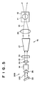
- the oscillation wavelength stabilizing means 30 comprises a ⁇ /2 plate 31 which controls the polarization of the light beam 13, a beam splitter 32 which reflects a part of the light beam 13 passing through the ⁇ /2 plate 31 and transmits the other part of the light beam 13 and a reflective grating 33 which disposed to receive the light beam 13R reflected by the beam splitter 32.
- the light beam 13R impinging upon the reflective grating 33 is selected by wavelength into a beam having a very narrow spectral bandwidth by the grating 33 and the light beam thus obtained is reflected to retrace the path of the light beam 13R.
- the light beam 13R is fed back to the semiconductor laser 14 through the beam splitter 32 and the ⁇ /2 plate 31.
- an external resonator is formed by the rear end face (the left end face as shown in Figure 1) of the semiconductor laser 14 and the reflective grating 33 and the oscillation wavelength of the semiconductor laser 14 is locked to the wavelength selected by the reflective grating 33.
- the oscillation wavelength stabilizing means 30A in the second embodiment is formed by a partial reflection type grating 34 which doubles the beam feedback optical system and the wavelength selector.
- the partial reflection type grating 34 is disposed on the optical path of the light beam 13 traveling from the semiconductor laser 14 to the prism 10 and reflects a part of the light beam 13 toward the semiconductor laser 14.
- the reflected light beam 13 is fed back to the semiconductor laser 14 and the oscillation wavelength of the semiconductor laser 14 is locked to the wavelength selected by the partial reflection type grating 34.
- the oscillation wavelength stabilizing means 30B in the third embodiment is formed by a reflective grating 33 and a collimator lens 35.
- the reflective grating 33 forms a beam feedback optical system together with the collimator lens 35 and doubles as a wavelength selector. That is, a rearward light beam 13Q emitted from the semiconductor laser 14 in the direction opposite to the light beam traveling from the semiconductor laser 14 to the prism 10 is collimated by the collimator lens 35 and impinges upon the reflective grating 33.
- the reflected light beam 13Q reflected by the reflective grating 33 is fed back to the semiconductor laser 14 and the oscillation wavelength of the semiconductor laser 14 is locked to the wavelength selected by the reflective grating 33.
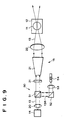
- the oscillation wavelength stabilizing means 40 in the fourth embodiment comprises a combination of a beam feedback optical system comprising a beam splitter 32 which is disposed on the optical path of the light beam 13 traveling from the semiconductor laser 14 to the prism 10 and splits a part of the laser beam 13, a narrow-band pass filter 41 which is disposed in a position where the light beam 13 split by the beam splitter 32 passes therethrough, a condenser lens 42 which converges the light beam 13R passing through the filter 41 and a mirror 43 on which the light beam 13R is converged by the condenser lens 42.
- a beam feedback optical system comprising a beam splitter 32 which is disposed on the optical path of the light beam 13 traveling from the semiconductor laser 14 to the prism 10 and splits a part of the laser beam 13, a narrow-band pass filter 41 which is disposed in a position where the light beam 13 split by the beam splitter 32 passes therethrough, a condenser lens 42 which converges the light beam 13R passing through the filter 41 and a mirror
- the light beam 13R is selected by wavelength into a beam having a very narrow spectral bandwidth by the filter 41 and the light beam thus obtained is reflected by the mirror 43 to retrace the path of the light beam 13R.
- the light beam is fed back to the semiconductor laser 14 through the beam splitter 32 and the ⁇ /2 plate 31.
- the oscillation wavelength of the semiconductor laser 14 is locked to the wavelength selected by the narrow-band pass filter 41.
- a half-silvered mirror can be employed in place of the beam splitter 32.
- the oscillation wavelength stabilizing means 40A in the fifth embodiment comprises a narrow-band pass filter 41, a condenser lens 44, a half-silvered mirror 45 and a collimator lens 46 which are disposed in this order on the optical path of the light beam 13 traveling from the semiconductor laser 14 to the prism 10.
- the condenser lens 44 and the half-silvered mirror 45 forms a beam feedback optical system. That is, a part of the light beam 13 is reflected by the half-silvered mirror 45 which is disposed so that the light beam 13 is converged thereon by the condenser lens 44 and is fed back to the semiconductor laser 14.
- the light beam 13 is selected by wavelength into a beam having a very narrow spectral bandwidth by the filter 41 and the light beam thus obtained is fed back to the semiconductor laser 14.
- the oscillation wavelength of the semiconductor laser 14 is locked to the wavelength selected by the narrow-band pass filter 41.
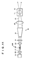
- the oscillation wavelength stabilizing means 40B in the sixth embodiment comprises a collimator lens 47 which collimates a rearward light beam 13Q from the semiconductor laser 14, a narrow-band pass filter 41 through which the collimated rearward light beam 13Q passes, a condenser lens 42 which converges the light beam 13Q passing through the filter 41 and a mirror 43 on which the light beam 13Q is converged by the condenser lens 42.
- the condenser lens 42 and the mirror 43 form a beam feedback optical system and the narrow-band filter 41 forms a wavelength selector. That is, the light beam 13Q is selected by wavelength into a beam having a very narrow spectral bandwidth by the filter 41 and the light beam thus obtained is fed back to the semiconductor laser 14. Thus the oscillation wavelength of the semiconductor laser 14 is locked to the wavelength selected by the narrow-band pass filter 41.
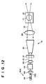
- the oscillation wavelength stabilizing means 50 in the seventh embodiment comprises a beam splitter 51 which is disposed on the optical path of the light beam 13 traveling from the semiconductor laser 14 to the prism 10 and splits a part of the laser beam 13, a mirror 52 which reflects the light beam 13R split by the beam splitter 51, a condenser lens 53 which converges the light beam 13R reflected by the mirror 52 and a reflective fiber grating 54 on one end face of which the light beam 13R is converged by the condenser lens 53.
- the reflective fiber grating 54 comprises a clad and a core which has a refractive index higher than that of the clad and is embedded in the clad.
- a plurality of refractive index varying portions are formed in the core at regular intervals.
- the reflective fiber grating 54 is formed by forming interference fringes in the core of an optical communication fiber (125 ⁇ m in the outer diameter of the clad and about 10 ⁇ m in the diameter of the core) by two-beam interference with excimer laser beams in ultraviolet region, thereby changing (increasing) the refractive indices of the parts of the core exposed to the leaser beams. It is supposed that the change in the refractive index is caused by chemical chance of germanium oxide, with which the core is doped, upon exposure to ultraviolet rays.
- the light beam 13R condensed by the condenser lens 53 enters the core through the end face of the reflective fiber grating 54 and propagates through the core.
- the aforesaid refractive index varying portions forms a grating along the direction in which the light beam 13R propagates.
- the grating reflects and diffracts only light of a specific wavelength corresponding to the period of the refractive index varying portions out of the light beam 13R propagating through the grating and feeds back the light of the specific wavelength back to the semiconductor laser 14, whereby the oscillation wavelength of the semiconductor laser 14 is locked to the wavelength selected by the reflective fiber grating 54.
- the oscillation wavelength stabilizing means 50A in the eighth embodiment comprises a condenser lens 55 which condenses the light beam 13 emitted from the semiconductor laser 14 and first and second fibers 56 and 57 which form a fiber coupler.
- the first fiber 56 has refractive index varying portions such as those described above and the second fiber 57 is jointed to the first fiber 56.
- a part of the light beam 13 which enters the second fiber 57 through an end face of the second fiber 57 and propagates along the second fiber 57 is transferred to the first fiber 56.
- the part of the light beam 13 which propagates through the second fiber 57 and emitted through the other end face of the second fiber 57 is used for analysis of the sample.
- the part of the light beam 13 transferred to the first fiber 56 propagates along the first fiber 56 and is reflected and refracted by the refractive index varying portions.
- the part of the light beam 13 reflected and refracted by the refractive index varying portions is fed back to the semiconductor laser 14 through the condenser lens 55, whereby the oscillation wavelength of the semiconductor laser 14 is locked to the wavelength selected by the first fiber 56.
- the oscillation wavelength stabilizing means 50B in the ninth embodiment comprises a condenser lens 55 which condenses the light beam 13 emitted from the semiconductor laser 14 and a partial reflection type fiber grating 58 which is positioned so that the light beam 13 condensed by the condenser lens 55 is converged on an end face thereof.
- the partial reflection type fiber grating 58 is basically of the same structure as the reflective fiber grating 54 and reflects and diffracts only light of a specific wavelength corresponding to the period of the refractive index varying portions out of the light beam 13 propagating through the core and feeds back the light of the specific wavelength back to the semiconductor laser 14, whereby the oscillation wavelength of the semiconductor laser 14 is locked to the wavelength selected by the partial reflection type fiber grating 58.
- the part of the light beam 13 which passes through the partial reflection type fiber grating 58 is used for analysis of the sample.
- the oscillation wavelength stabilizing means 50C in the tenth embodiment comprises a condenser len5947 which converges a rearward light beam 13Q emitted from the semiconductor laser 14 and a reflective fiber grating 54 positioned so that the light beam 13Q is converged on one end face thereof by the condenser lens 59.
- the part of the rearward light beam 13Q reflected by the reflective fiber grating 54 is fed back to the semiconductor laser 14, whereby the oscillation wavelength of the semiconductor laser 14 is locked to the wavelength selected by the reflective fiber grating 54.
- the surface plasmon sensor in accordance with the eleventh embodiment of the present invention shown in Figure 13 basically differs from that shown in Figure 2 in that the metal film 12 is formed on a dielectric block 62 of a glass which is substantially rectangular in shape and is connected to the upper face of a prism 60 by way of refractive index matching fluid 61.
- the light beam 13 is caused to impinge upon the interface 62a of the dielectric block 62 and the metal film 12 through the prism 60 so that the light beam 13 is reflected in total reflection by the interface 62a.
- the dielectric block 62 and the prism 60 are formed of the same material and are connected by the refractive index matching fluid 61 which is equal to the material of the dielectric block 62 and the prism 60 in refractive index. Accordingly the system of the dielectric block 62 and the prism 60 is optically equivalent to the single prism 10.
- the oscillation wavelength of the laser is stabilized by feedback of the laser beam, it is possible to stabilize the oscillation wavelength of the laser without feeding back the laser beam.
- a laser such as a DFB (distributed feedback) laser or a DBR (distributed Bragg reflector) laser or the like which has an oscillation wavelength stabilizing means per se may be used as the light source.
- oscillation wavelength stabilizing means may be a means for electrically controlling the laser drive current and/or the temperature of the laser.
- the present invention can be applied also to a plasmon sensor in which a layer of a material which is specifically coupled to a material to be measured is formed on a metal film and only a specific material is detected (e.g., a plasmon sensor for detecting antigen-antibody reaction), a plasmon sensor which measures the two-dimensional distribution of physical properties of a sample placed on a metal film, and the like.
- a plasmon sensor in which a layer of a material which is specifically coupled to a material to be measured is formed on a metal film and only a specific material is detected
- a plasmon sensor for detecting antigen-antibody reaction e.g., a plasmon sensor for detecting antigen-antibody reaction
- a plasmon sensor which measures the two-dimensional distribution of physical properties of a sample placed on a metal film, and the like.
Landscapes
- Physics & Mathematics (AREA)
- Health & Medical Sciences (AREA)
- Life Sciences & Earth Sciences (AREA)
- Chemical & Material Sciences (AREA)
- Analytical Chemistry (AREA)
- Biochemistry (AREA)
- General Health & Medical Sciences (AREA)
- General Physics & Mathematics (AREA)
- Immunology (AREA)
- Pathology (AREA)
- Investigating Or Analysing Materials By Optical Means (AREA)
Applications Claiming Priority (4)
| Application Number | Priority Date | Filing Date | Title |
|---|---|---|---|
| JP2414798 | 1998-02-05 | ||
| JP2414798 | 1998-02-05 | ||
| JP25957798 | 1998-09-14 | ||
| JP25957798 | 1998-09-14 |
Publications (2)
| Publication Number | Publication Date |
|---|---|
| EP0935131A2 true EP0935131A2 (de) | 1999-08-11 |
| EP0935131A3 EP0935131A3 (de) | 2000-03-15 |
Family
ID=26361632
Family Applications (1)
| Application Number | Title | Priority Date | Filing Date |
|---|---|---|---|
| EP99102150A Ceased EP0935131A3 (de) | 1998-02-05 | 1999-02-03 | Oberflächenplasmonenresonanz-Sensor mit wellenlängenstabilisierter Laserlichtquelle |
Country Status (2)
| Country | Link |
|---|---|
| US (1) | US6340448B1 (de) |
| EP (1) | EP0935131A3 (de) |
Cited By (3)
| Publication number | Priority date | Publication date | Assignee | Title |
|---|---|---|---|---|
| EP1219952A1 (de) * | 2000-12-25 | 2002-07-03 | Fuji Photo Film Co., Ltd. | Sensor unter Verwendung von abgeschwächter Totalreflektion |
| CN101802592B (zh) * | 2007-08-20 | 2013-01-09 | 韩国生命工学研究院 | 使用旋转镜的表面等离子共振传感器 |
| GB2517955A (en) * | 2013-09-05 | 2015-03-11 | Nat Univ Chung Cheng | Optical waveguide particle plasmon resonance sensing system |
Families Citing this family (6)
| Publication number | Priority date | Publication date | Assignee | Title |
|---|---|---|---|---|
| US6697158B2 (en) * | 2001-04-03 | 2004-02-24 | Fuji Photo Film Co., Ltd. | Measuring apparatus utilizing attenuated total reflection |
| KR20040012384A (ko) * | 2002-08-03 | 2004-02-11 | 이종협 | 고감도 표면 플라즈몬 공명장치와 이를 이용한 중금속의흡착과 선택도의 측정방법 |
| US7151597B2 (en) * | 2003-12-05 | 2006-12-19 | Agilent Technologie, Inc | Optical wavelength standard and optical wavelength calibration system and method |
| DE102004033869B3 (de) * | 2004-07-13 | 2006-03-30 | Gesellschaft zur Förderung der Spektrochemie und angewandten Spektroskopie e.V. | Verfahren zur Bestimmung von Oberflächenplasmonenresonanzen an zweidimensionalen Messflächen |
| US7406222B2 (en) * | 2006-02-16 | 2008-07-29 | Pavel Kornilovich | Composite evanescent waveguides and associated methods |
| JP5949905B2 (ja) * | 2012-03-26 | 2016-07-13 | コニカミノルタ株式会社 | プリズム及びセンサーチップ |
Citations (4)
| Publication number | Priority date | Publication date | Assignee | Title |
|---|---|---|---|---|
| EP0577285A1 (de) * | 1992-06-17 | 1994-01-05 | Hewlett-Packard Company | Geräte zur Messung der Oberflächen-plasmonenresonanz |
| WO1995022754A1 (en) * | 1994-02-16 | 1995-08-24 | Valtion Teknillinen Tutkimuskeskus | Device for carrying out an analysis |
| US5619523A (en) * | 1995-09-08 | 1997-04-08 | David Sarnoff Research Center, Inc. | Semiconductor distributed feedback laser diode |
| US5629774A (en) * | 1991-09-19 | 1997-05-13 | British Gas Plc | Optical sensor |
Family Cites Families (9)
| Publication number | Priority date | Publication date | Assignee | Title |
|---|---|---|---|---|
| DE2606991A1 (de) * | 1976-02-20 | 1977-08-25 | Nils Dr Med Kaiser | Geraet zur bestimmung des gehaltes von stoffwechselprodukten im blut |
| FI85768C (fi) * | 1990-07-04 | 1992-05-25 | Valtion Teknillinen | Foerfarande foer utfoerning av ytplasmonresonansmaetning samt i foerfarandet anvaendbar givare. |
| JPH06167443A (ja) | 1992-10-23 | 1994-06-14 | Olympus Optical Co Ltd | 表面プラズモン共鳴を利用した測定装置 |
| EP0679250B1 (de) * | 1993-11-15 | 2000-03-15 | CARL ZEISS JENA GmbH | Anordnung zur analyse von substanzen an der oberfläche eines optischen sensors |
| US5917607A (en) * | 1996-04-25 | 1999-06-29 | Fuji Photo Film Co., Ltd. | Surface plasmon sensor for multiple channel analysis |
| EP0805347A3 (de) * | 1996-04-30 | 1998-08-05 | Fuji Photo Film Co., Ltd. | Oberflächen-Plasmon-Sensor |
| DE69830529T2 (de) * | 1997-02-07 | 2006-05-11 | Fuji Photo Film Co., Ltd., Minami-Ashigara | Oberflächen-Plasmonen-Sensor |
| US5926284A (en) * | 1997-04-30 | 1999-07-20 | Fuji Photo Film Co., Ltd. | Surface plasmon sensor |
| JP3343086B2 (ja) * | 1998-04-28 | 2002-11-11 | 富士写真フイルム株式会社 | 表面プラズモンセンサー |
-
1999
- 1999-02-03 EP EP99102150A patent/EP0935131A3/de not_active Ceased
- 1999-02-05 US US09/245,068 patent/US6340448B1/en not_active Expired - Lifetime
Patent Citations (4)
| Publication number | Priority date | Publication date | Assignee | Title |
|---|---|---|---|---|
| US5629774A (en) * | 1991-09-19 | 1997-05-13 | British Gas Plc | Optical sensor |
| EP0577285A1 (de) * | 1992-06-17 | 1994-01-05 | Hewlett-Packard Company | Geräte zur Messung der Oberflächen-plasmonenresonanz |
| WO1995022754A1 (en) * | 1994-02-16 | 1995-08-24 | Valtion Teknillinen Tutkimuskeskus | Device for carrying out an analysis |
| US5619523A (en) * | 1995-09-08 | 1997-04-08 | David Sarnoff Research Center, Inc. | Semiconductor distributed feedback laser diode |
Cited By (5)
| Publication number | Priority date | Publication date | Assignee | Title |
|---|---|---|---|---|
| EP1219952A1 (de) * | 2000-12-25 | 2002-07-03 | Fuji Photo Film Co., Ltd. | Sensor unter Verwendung von abgeschwächter Totalreflektion |
| US6741352B2 (en) | 2000-12-25 | 2004-05-25 | Fuji Photo Film Co., Ltd. | Sensor utilizing attenuated total reflection |
| CN101802592B (zh) * | 2007-08-20 | 2013-01-09 | 韩国生命工学研究院 | 使用旋转镜的表面等离子共振传感器 |
| GB2517955A (en) * | 2013-09-05 | 2015-03-11 | Nat Univ Chung Cheng | Optical waveguide particle plasmon resonance sensing system |
| GB2517955B (en) * | 2013-09-05 | 2016-06-08 | Nat Univ Chung Cheng | Optical waveguide particle plasmon resonance sensing system |
Also Published As
| Publication number | Publication date |
|---|---|
| US6340448B1 (en) | 2002-01-22 |
| EP0935131A3 (de) | 2000-03-15 |
Similar Documents
| Publication | Publication Date | Title |
|---|---|---|
| US6819812B2 (en) | System and method for measuring physical, chemical and biological stimuli using vertical cavity surface emitting lasers with integrated tuner | |
| US6323987B1 (en) | Controlled multi-wavelength etalon | |
| US5442169A (en) | Method and apparatus for determining a measuring variable by means of an integrated optical sensor module | |
| US8857242B2 (en) | Photoacoustic gas sensor and its use | |
| EP1075651B1 (de) | Verfahren zur anregung eines optischen resonators zum nachweis von gasspuren | |
| US6411639B1 (en) | Semiconductor laser module with an external resonator including a band-pass filter and reflective element | |
| EP1060383A2 (de) | Wellenleiterstruktur | |
| US7355162B2 (en) | Optical wavelength measuring device using guiding body and diffractive structure | |
| EP1308714B1 (de) | Messplatte zur Verwendung in einem auf dem Prinzip der abgeschwächten Totalreflexion basierenden Sensor | |
| EP0935131A2 (de) | Oberflächenplasmonenresonanz-Sensor mit wellenlängenstabilisierter Laserlichtquelle | |
| KR20170098518A (ko) | 광센서 | |
| US5875032A (en) | Surface plasmon sensor having an improved optical system | |
| EP1219952B1 (de) | Sensor unter Verwendung von abgeschwächter Totalreflektion | |
| JP4885494B2 (ja) | 波長可変レーザ光源 | |
| JP2003069133A (ja) | 微細多共振器を利用した波長固定集積光源構造 | |
| US6697158B2 (en) | Measuring apparatus utilizing attenuated total reflection | |
| US4644556A (en) | Extended laser sensor | |
| US20030227949A1 (en) | Integrated, temperature insensitive wavelength locker for use in laser packages | |
| JP3390355B2 (ja) | 表面プラズモンセンサー | |
| JP3844688B2 (ja) | 全反射減衰を利用したセンサー | |
| US6829052B2 (en) | Sensor detecting attenuated total reflection angle by using semiconductor laser unit driven with driving current on which high frequency component is superimposed | |
| US20020081065A1 (en) | Fabry-perot etalon, wavelength measuring apparatus, and wavelength tunable light source device with built-in wavelength measuring apparatus | |
| JPH03249502A (ja) | 光センサ | |
| JPH0789147B2 (ja) | 距離測定装置 | |
| JPH1197792A (ja) | 可変波長半導体レーザ光源 |
Legal Events
| Date | Code | Title | Description |
|---|---|---|---|
| PUAI | Public reference made under article 153(3) epc to a published international application that has entered the european phase |
Free format text: ORIGINAL CODE: 0009012 |
|
| AK | Designated contracting states |
Kind code of ref document: A2 Designated state(s): DE FR GB |
|
| AX | Request for extension of the european patent |
Free format text: AL;LT;LV;MK;RO;SI |
|
| PUAL | Search report despatched |
Free format text: ORIGINAL CODE: 0009013 |
|
| AK | Designated contracting states |
Kind code of ref document: A3 Designated state(s): AT BE CH CY DE DK ES FI FR GB GR IE IT LI LU MC NL PT SE |
|
| AX | Request for extension of the european patent |
Free format text: AL;LT;LV;MK;RO;SI |
|
| 17P | Request for examination filed |
Effective date: 20000413 |
|
| AKX | Designation fees paid |
Free format text: DE FR GB |
|
| 17Q | First examination report despatched |
Effective date: 20060913 |
|
| RAP1 | Party data changed (applicant data changed or rights of an application transferred) |
Owner name: FUJIFILM CORPORATION |
|
| STAA | Information on the status of an ep patent application or granted ep patent |
Free format text: STATUS: THE APPLICATION HAS BEEN REFUSED |
|
| 18R | Application refused |
Effective date: 20091115 |