EP0935283A2 - Silikonpolymerisolationsfilm auf einem Halbleitersubstrat und seine Herstellungsmethode - Google Patents
Silikonpolymerisolationsfilm auf einem Halbleitersubstrat und seine Herstellungsmethode Download PDFInfo
- Publication number
- EP0935283A2 EP0935283A2 EP99300841A EP99300841A EP0935283A2 EP 0935283 A2 EP0935283 A2 EP 0935283A2 EP 99300841 A EP99300841 A EP 99300841A EP 99300841 A EP99300841 A EP 99300841A EP 0935283 A2 EP0935283 A2 EP 0935283A2
- Authority
- EP
- European Patent Office
- Prior art keywords
- gas
- dielectric constant
- film
- silicon
- relative dielectric
- Prior art date
- Legal status (The legal status is an assumption and is not a legal conclusion. Google has not performed a legal analysis and makes no representation as to the accuracy of the status listed.)
- Withdrawn
Links
Images

Classifications
-
- H—ELECTRICITY
- H10—SEMICONDUCTOR DEVICES; ELECTRIC SOLID-STATE DEVICES NOT OTHERWISE PROVIDED FOR
- H10P—GENERIC PROCESSES OR APPARATUS FOR THE MANUFACTURE OR TREATMENT OF DEVICES COVERED BY CLASS H10
- H10P14/00—Formation of materials, e.g. in the shape of layers or pillars
- H10P14/60—Formation of materials, e.g. in the shape of layers or pillars of insulating materials
-
- B—PERFORMING OPERATIONS; TRANSPORTING
- B05—SPRAYING OR ATOMISING IN GENERAL; APPLYING FLUENT MATERIALS TO SURFACES, IN GENERAL
- B05D—PROCESSES FOR APPLYING FLUENT MATERIALS TO SURFACES, IN GENERAL
- B05D1/00—Processes for applying liquids or other fluent materials
- B05D1/62—Plasma-deposition of organic layers
-
- C—CHEMISTRY; METALLURGY
- C09—DYES; PAINTS; POLISHES; NATURAL RESINS; ADHESIVES; COMPOSITIONS NOT OTHERWISE PROVIDED FOR; APPLICATIONS OF MATERIALS NOT OTHERWISE PROVIDED FOR
- C09D—COATING COMPOSITIONS, e.g. PAINTS, VARNISHES OR LACQUERS; FILLING PASTES; CHEMICAL PAINT OR INK REMOVERS; INKS; CORRECTING FLUIDS; WOODSTAINS; PASTES OR SOLIDS FOR COLOURING OR PRINTING; USE OF MATERIALS THEREFOR
- C09D4/00—Coating compositions, e.g. paints, varnishes or lacquers, based on organic non-macromolecular compounds having at least one polymerisable carbon-to-carbon unsaturated bond ; Coating compositions, based on monomers of macromolecular compounds of groups C09D183/00 - C09D183/16
-
- C—CHEMISTRY; METALLURGY
- C23—COATING METALLIC MATERIAL; COATING MATERIAL WITH METALLIC MATERIAL; CHEMICAL SURFACE TREATMENT; DIFFUSION TREATMENT OF METALLIC MATERIAL; COATING BY VACUUM EVAPORATION, BY SPUTTERING, BY ION IMPLANTATION OR BY CHEMICAL VAPOUR DEPOSITION, IN GENERAL; INHIBITING CORROSION OF METALLIC MATERIAL OR INCRUSTATION IN GENERAL
- C23C—COATING METALLIC MATERIAL; COATING MATERIAL WITH METALLIC MATERIAL; SURFACE TREATMENT OF METALLIC MATERIAL BY DIFFUSION INTO THE SURFACE, BY CHEMICAL CONVERSION OR SUBSTITUTION; COATING BY VACUUM EVAPORATION, BY SPUTTERING, BY ION IMPLANTATION OR BY CHEMICAL VAPOUR DEPOSITION, IN GENERAL
- C23C16/00—Chemical coating by decomposition of gaseous compounds, without leaving reaction products of surface material in the coating, i.e. chemical vapour deposition [CVD] processes
- C23C16/22—Chemical coating by decomposition of gaseous compounds, without leaving reaction products of surface material in the coating, i.e. chemical vapour deposition [CVD] processes characterised by the deposition of inorganic material, other than metallic material
- C23C16/30—Deposition of compounds, mixtures or solid solutions, e.g. borides, carbides, nitrides
- C23C16/40—Oxides
- C23C16/401—Oxides containing silicon
-
- H—ELECTRICITY
- H10—SEMICONDUCTOR DEVICES; ELECTRIC SOLID-STATE DEVICES NOT OTHERWISE PROVIDED FOR
- H10W—GENERIC PACKAGES, INTERCONNECTIONS, CONNECTORS OR OTHER CONSTRUCTIONAL DETAILS OF DEVICES COVERED BY CLASS H10
- H10W74/00—Encapsulations, e.g. protective coatings
- H10W74/40—Encapsulations, e.g. protective coatings characterised by their materials
- H10W74/47—Encapsulations, e.g. protective coatings characterised by their materials comprising organic materials, e.g. plastics or resins
- H10W74/476—Organic materials comprising silicon
-
- H—ELECTRICITY
- H10—SEMICONDUCTOR DEVICES; ELECTRIC SOLID-STATE DEVICES NOT OTHERWISE PROVIDED FOR
- H10P—GENERIC PROCESSES OR APPARATUS FOR THE MANUFACTURE OR TREATMENT OF DEVICES COVERED BY CLASS H10
- H10P14/00—Formation of materials, e.g. in the shape of layers or pillars
- H10P14/60—Formation of materials, e.g. in the shape of layers or pillars of insulating materials
- H10P14/63—Formation of materials, e.g. in the shape of layers or pillars of insulating materials characterised by the formation processes
- H10P14/6326—Deposition processes
- H10P14/6328—Deposition from the gas or vapour phase
- H10P14/6334—Deposition from the gas or vapour phase using decomposition or reaction of gaseous or vapour phase compounds, i.e. chemical vapour deposition
- H10P14/6336—Deposition from the gas or vapour phase using decomposition or reaction of gaseous or vapour phase compounds, i.e. chemical vapour deposition in the presence of a plasma [PECVD]
-
- H—ELECTRICITY
- H10—SEMICONDUCTOR DEVICES; ELECTRIC SOLID-STATE DEVICES NOT OTHERWISE PROVIDED FOR
- H10P—GENERIC PROCESSES OR APPARATUS FOR THE MANUFACTURE OR TREATMENT OF DEVICES COVERED BY CLASS H10
- H10P14/00—Formation of materials, e.g. in the shape of layers or pillars
- H10P14/60—Formation of materials, e.g. in the shape of layers or pillars of insulating materials
- H10P14/66—Formation of materials, e.g. in the shape of layers or pillars of insulating materials characterised by the type of materials
- H10P14/668—Formation of materials, e.g. in the shape of layers or pillars of insulating materials characterised by the type of materials the materials being characterised by the deposition precursor materials
- H10P14/6681—Formation of materials, e.g. in the shape of layers or pillars of insulating materials characterised by the type of materials the materials being characterised by the deposition precursor materials the precursor containing a compound comprising Si
- H10P14/6684—Formation of materials, e.g. in the shape of layers or pillars of insulating materials characterised by the type of materials the materials being characterised by the deposition precursor materials the precursor containing a compound comprising Si the compound comprising silicon and oxygen
- H10P14/6686—Formation of materials, e.g. in the shape of layers or pillars of insulating materials characterised by the type of materials the materials being characterised by the deposition precursor materials the precursor containing a compound comprising Si the compound comprising silicon and oxygen the compound being a molecule comprising at least one silicon-oxygen bond and the compound having hydrogen or an organic group attached to the silicon or oxygen, e.g. a siloxane
-
- H—ELECTRICITY
- H10—SEMICONDUCTOR DEVICES; ELECTRIC SOLID-STATE DEVICES NOT OTHERWISE PROVIDED FOR
- H10P—GENERIC PROCESSES OR APPARATUS FOR THE MANUFACTURE OR TREATMENT OF DEVICES COVERED BY CLASS H10
- H10P14/00—Formation of materials, e.g. in the shape of layers or pillars
- H10P14/60—Formation of materials, e.g. in the shape of layers or pillars of insulating materials
- H10P14/69—Inorganic materials
- H10P14/692—Inorganic materials composed of oxides, glassy oxides or oxide-based glasses
- H10P14/6921—Inorganic materials composed of oxides, glassy oxides or oxide-based glasses containing silicon
- H10P14/6922—Inorganic materials composed of oxides, glassy oxides or oxide-based glasses containing silicon the material containing Si, O and at least one of H, N, C, F or other non-metal elements, e.g. SiOC, SiOC:H or SiONC
-
- Y—GENERAL TAGGING OF NEW TECHNOLOGICAL DEVELOPMENTS; GENERAL TAGGING OF CROSS-SECTIONAL TECHNOLOGIES SPANNING OVER SEVERAL SECTIONS OF THE IPC; TECHNICAL SUBJECTS COVERED BY FORMER USPC CROSS-REFERENCE ART COLLECTIONS [XRACs] AND DIGESTS
- Y10—TECHNICAL SUBJECTS COVERED BY FORMER USPC
- Y10S—TECHNICAL SUBJECTS COVERED BY FORMER USPC CROSS-REFERENCE ART COLLECTIONS [XRACs] AND DIGESTS
- Y10S257/00—Active solid-state devices, e.g. transistors, solid-state diodes
- Y10S257/914—Polysilicon containing oxygen, nitrogen, or carbon, e.g. sipos
Definitions
- This invention relates generally to a semiconductor technique and more particularly to a silicone polymer insulation film on a semiconductor substrate and a method for forming the film by using a plasma CVD (chemical vapor deposition) apparatus.
- a plasma CVD chemical vapor deposition
- Conventional silicon oxide films SiO x are produced by a method in which oxygen O 2 or nitrogen oxide N 2 O is added as an oxidizing agent to a silicon material gas such as SiH 4 or Si(OC 2 H 5 ) 4 and then processed by heat or plasma energy. Its relative dielectric constant is about 4.0.
- a fluorinated amorphous carbon film has been produced from C x F y H z as a material gas by a plasma CVD method. Its relative dielectric constant ⁇ is as low as 2.0-2.4.
- a silicon-containing organic film is produced from a material gas under low pressure (1 Torr) by the plasma CVD method.
- the material gas is made from P-TMOS (phenyl trimethoxysilane, formula 1), which is a compound of benzene and silicon, vaporized by a babbling method.
- the relative dielectric constant ⁇ of this film is as low as 3.1.
- a further method uses a porous structure made in the film.
- An insulation film- is produced from an inorganic SOG material by a spin-coat method.
- the relative dielectric constant ⁇ of the film is as low as 2.3.
- the fluorinated amorphous carbon film has lower thermal stability (370°C), poor adhesion with silicon-containing materials and also lower mechanical strength.
- the lower thermal stability leads to damage under high temperatures such as over 400°C. Poor adhesion may cause the film to peel off easily. Further, the lower mechanical strength can jeopardize wiring materials.
- Oligomers that are polymerized using P-TMOS molecules do not form a linear structure in the vapor phase, such as a siloxane structure, because the P-TMOS molecule has three O-CH 3 bonds.
- the oligomers having no linear structure cannot form a porous structure on a Si substrate, i.e., the density of the deposited film cannot be reduced. As a result, the relative dielectric constant of the film cannot be reduced to a desired degree.
- the babbling method means a method wherein vapor of a liquid material, which is obtained by having a carrier gas such as argon gas pass through the material, is introduced into a reaction chamber with the carrier gas.
- This method generally requires a large amount of a carrier gas in order to cause the material gas to flow. As a result, the material gas cannot stay in the reaction chamber for a sufficient length of time to cause polymerization in a vapor phase.
- the SOG insulation film of the spin-coat method has a problem in that the material cannot be applied onto the silicon substrate evenly and another problem in which a cure system after the coating process is costly.
- One aspect of this invention involves a method for forming an insulation film on a semiconductor substrate by using a plasma CVD apparatus including a reaction chamber, which method comprises a step of directly vaporizing a silicon-containing hydrocarbon compound expressed by the general formula Si ⁇ O ⁇ C x H y ( ⁇ , ⁇ , x , and y are integers) and then introducing it to the reaction chamber of the plasma CVD apparatus, a step of introducing an additive gas, the flow volume of which is substantially reduced, into the reaction chamber and also a step of forming an insulation film on a semiconductor substrate by plasma polymerization reaction wherein mixed gases made from the vaporized silicon-containing hydrocarbon compound as a material gas and the additive gas are used as a reaction gas. It is a remarkable feature that the reduction of the additive gas flow also results in a substantial reduction of the total flow of the reaction gas. According to the present invention, a silicone polymer film having a micropore porous structure with low relative dielectric constant can be produced.
- the present invention is also drawn to an insulation film formed on a semiconductor substrate, and a material for forming the insulation film, residing in the features described above.
- Figure 1 is a schematic diagram illustrating a plasma CVD apparatus used for forming an insulation film of this invention.
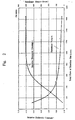
- Figure 2 is a graph showing the relationship between relative dielectric constant and the total flow of a reaction gas as well as the relationship between residence time and the total flow of a reaction gas, both in experiments using PM-DMOS as a material gas.
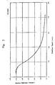
- Figure 3 is a graph showing the relationship between the residence time and relative dielectric constant in experiments using PM-DMOS as a material gas.
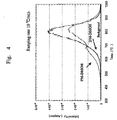
- Figure 4 is a graph showing the thermal desorption spectra of components having a molecular weight of 16 due to desorption of CH 4 from films (PM-DMOS, DM-DMOS) according to the present invention in a thermal desorption test.
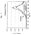
- Figure 5 is a graph showing changes in the degree of vacuum corresponding to the number of total molecules desorpted from the films (PM-DMOS, DM-DMOS), i.e., pressure raises due to gas desorpted from the films in the thermal desorption test.
- the silicon-containing hydrocarbon compound expressed as the general formula Si ⁇ O ⁇ C x H y ( ⁇ , ⁇ , x, and y are integers) is preferably a compound having at least one Si-O bond, two or less O-C n H 2n+1 bonds and at least two hydrocarbon radicals bonded with silicon (Si). More specifically, the silicon-containing hydrocarbon compound includes at least one species of the compound expressed by the chemical formula (2) as follows: wherein R1 and R2 are one of CH 3 , C 2 H 3 , C 2 H 5 , C 3 H 7 and C 6 H 5 , and m and n are any integer.
- the silicon-containing hydrocarbon compound can include at least one species of the compound expressed by the chemical formula (3) as follows: wherein R1, R2 and R3 are one of CH 3 , C 2 H 3 , C 2 H 5 , C 3 H 7 and C 6 H 5 , and n is any integer.
- the silicon-containing hydrocarbon compound can include at least one species of the compound expressed by the chemical formula (4) as follows: wherein R1, R2, R3 and R4 are one of CH 3 , C 2 H 3 , C 2 H 5 , C 3 H 7 and C 6 H 5 , and m and n are any integer.
- the silicon-containing hydrocarbon compound can include at least one species of the compound expressed by the chemical formula (5) as follows: wherein R1, R2, R3, R4, R5 and R6 are one of CH 3 , C 2 H 3 , C 2 H 5 , C 3 H 7 and C 6 H 5 , and the additive gases are argon (Ar), Helium (He) and either nitrogen oxide (N 2 O) or oxygen (O 2 ).
- the silicon-containing hydrocarbon compound can include at least one species of the compound expressed by the chemical formula (6) as follows: wherein R1, R2, R3 and R4 are one of CH 3 , C 2 H 3 , C 2 H 5 , C 3 H 7 and C 6 H 5 , and the additive gases are argon (Ar), Helium (He) and either nitrogen oxide (N 2 O) or oxygen (O 2 ).
- the material gas can include at least one of said silicon-containing hydrocarbon compounds indicated above.
- an insulation film is formed on a substrate and the film is polymerized with plasma energy in a plasma CVD apparatus by using a material gas including a silicon-containing hydrocarbon compound expressed by formula 2.
- the insulation film is formed on a substrate and the film is polymerized with plasma energy in a plasma CVD apparatus by using a material gas including a silicon-containing hydrocarbon compound expressed by formula 3.
- the insulation film is formed on a substrate and the film is polymerized with plasma energy in a plasma CVD apparatus by using a material gas including a silicon-containing hydrocarbon compound expressed by formula 4.
- the insulation film is formed on a substrate and the film is polymerized with plasma energy in a plasma CVD apparatus by using a material gas including a silicon-containing hydrocarbon compound expressed by formula 5.
- the insulation film is formed on a substrate and the film is polymerized with plasma energy in a plasma CVD apparatus by using a material gas including a silicon-containing hydrocarbon compound expressed by formula 6.
- a material for forming an insulation film is supplied in a vapor phase in the vicinity of a substrate and is treated in a plasma CVD apparatus to form the insulation film on the substrate by chemical reaction, and the material is further expressed by formula 2.
- a material for forming an insulation film is supplied in a vapor phase in the vicinity of a substrate and is treated in a plasma CVD apparatus to form the insulation film on the substrate by chemical reaction, and the material is further expressed by formula 3.
- a material for forming an insulation film is supplied in a vapor phase in the vicinity of a substrate and is treated in a plasma CVD apparatus to form the insulation film on the substrate by chemical reaction, and the material is further expressed by formula 4.
- a material for forming an insulation film is supplied in a vapor phase with either nitrogen oxide (N 2 O) or oxygen (O 2 ) as an oxidizing agent in the vicinity of a substrate and is treated in a plasma CVD apparatus to form said insulation film on said substrate by chemical reaction, and this material can be the compound expressed by formula 5.
- a material for forming an insulation film is supplied in a vapor phase with either nitrogen oxide (N 2 O) or oxygen (O 2 ) as the oxidizing agent in the vicinity of a substrate and is treated in a plasma CVD apparatus to form said insulation film on said substrate by chemical reaction, and this material further can be the compound expressed by formula 6.
- the residence time of the reaction gas is determined based on the capacity of the reaction chamber for reaction, the pressure adapted for reaction, and the total flow of the reaction gas.
- the reaction pressure is normally in the range of 1-10 Torr, preferably 3-7 Torr, so as to maintain stable plasma. This reaction pressure is relatively high in order to lengthen the residence time of the reaction gas.
- the total flow of the reaction gas is important to reducing the relative dielectric constant of a resulting film. It is not necessary to control the ratio of the material gas to the additive gas. In general, the longer the residence time, the lower the relative dielectric constant becomes.
- the material gas flow necessary for forming a film depends on the desired deposition rate and the area of a substrate on which a film is formed.
- sccm the material gas
- the total flow can be defined by residence time (Rt).
- Rt residence time
- a preferred range of Rt is 100 msec ⁇ 1Rt, more preferably 200 msec ⁇ Rt ⁇ 5 sec.
- Rt is generally in the range of 10-30 msec.
- Rt[s] 9.42x10 7 (Pr ⁇ Ts/Ps ⁇ Tr)r w 2 d/F wherein:
- the residence time means the average period of time in which gas molecules stay in the reaction chamber.
- the space for reaction in the reaction chamber is defined by the surface of the substrate ( ⁇ r 2 ) and the space between the upper electrode and the lower electrode. Considering the gas flow through the space for reaction, ⁇ can be estimated as 1/2. In the above formula, ⁇ is 1/2.
- the material gas is, in short, a silicon-containing hydrocarbon compound including at least one Si-O bond, at most two O-C n H 2n+1 bonds and at least two hydrocarbon radicals bonded to the silicon (Si). Also, this material gas is vaporized by a direct vaporization method. The method results in an insulation film having a low relative dielectric constant, high thermal stability and high humidity-resistance.
- the material gas vaporized by the direct vaporization method can stay in the plasma for a sufficient length of time.
- a linear polymer can be formed so that a linear polymer having the basic structure (formula 7), wherein the "n" is 2 or a greater value, forms in a vapor phase.
- the polymer is then deposited on the semiconductor substrate and forms an insulation film having a micropore porous structure.
- X1 and X2 are O n C m H p wherein n is 0 or 1, m and p are integers including zero.
- the insulation film of this invention has a relatively high stability because its fundamental structure has the Si-O bond having high bonding energy therebetween. Also, its relative dielectric constant is low because it has a micropore porous structure. Further, the fundamental structure (-Si-O-) n has, on both sides, dangling bonds ending with a hydrocarbon radical possessing hydrophobicity, and this property renders the humidity-resistance. Furthermore, the bond of a hydrocarbon radical and silicon is generally stable. For instance, both the bond with a methyl radical, i.e., Si-CH 3 , and bond with benzene, i.e., Si-C 6 H 5 , have a dissociation temperature of 500°C or higher. Since above semiconductor production requires thermal stability to temperatures above 450°C, that property of the film is advantageous for production of semiconductors.
- FIG. 1 diagrammatically shows a plasma CVD apparatus usable in this invention.
- This apparatus comprises a reaction gas-supplying device 12 and a plasma CVD device 1.
- the reaction gas-supplying device 12 comprises plural lines 13, control valves 8 disposed in the lines 13, and gas inlet ports 14, 15 and 16.
- a flow controller 7 is connected to the individual control valves 8 for controlling a flow of a material gas of a predetermined volume.
- a container accommodating liquid reacting material 18 is connected to a vaporizer 17 that directly vaporizes liquid.
- the plasma CVD device 1 includes a reaction chamber 6, a gas inlet port 5, a susceptor 3 and a heater 2.
- a circular gas diffusing plate 10 is disposed immediately under the gas inlet port.
- the gas diffusing plate 10 has a number of fine openings at its bottom face and can inject reaction gas to the semiconductor substrate 4 therefrom.
- the susceptor 3 is placed in parallel with and facing the gas diffusing plate 10. The susceptor 3 holds a semiconductor substrate 4 thereon and heats it with the heater 2.
- the gas inlet port 5 is insulated from the reaction chamber 6 and connected to an outer high frequency power supply 9. Alternatively, the susceptor 3 can be connected to the power supply 9.
- the gas diffusing plate 10 and the susceptor 3 act as a high frequency electrode and generate a plasma reacting field in proximity to the surface of the semiconductor substrate 4.
- a method for forming an insulation film on a semiconductor substrate by using the plasma CVD apparatus of this invention comprises a step of directly vaporizing silicon-containing hydrocarbon compounds expressed by the general formula Si ⁇ O ⁇ C x H y ( ⁇ , ⁇ , x, and y are integers) and then introducing it to the reaction chamber 6 of the plasma CVD device 1, a step of introducing an additive gas, whose flow is substantially reduced, into the reaction chamber 6 and also a step of forming an insulation film on a semiconductor substrate by plasma polymerization reaction wherein mixed gases, made from the silicon-containing hydrocarbon compound as a material gas and the additive gas, are used as a reaction gas. It is a remarkable feature that the reduction of the additive gas flow also renders a substantial reduction of the total flow of the reaction gas. This feature will be described in more detail later.
- the silicon-containing hydrocarbon compound expressed as the general formula Si ⁇ O ⁇ C x H y ( ⁇ , ⁇ , x, and y are integers) is preferably a compound having at least one Si-O bond, two or less O-C n H 2n+1 bonds and at least two hydrocarbon radicals bonded with silicon (Si). More specifically, it is a compound indicated by
- silicon-containing hydrocarbon compound can be any combinations of these compounds and mixtures.
- the additive gases used in this embodiment are argon gas and helium gas.
- Argon is principally used for stabilizing plasma, while helium is used for improving uniformity of the plasma and also uniformity of thickness of the insulation film.
- the first step of direct vaporization is a method wherein a liquid material, the flow of which is controlled, is instantaneously vaporized at a vaporizer that is preheated.
- This direct vaporization method requires no carrier gas such as argon to obtain a designated amount of the material gas. This differs greatly with the babbling method. Accordingly, a large amount of argon gas or helium gas is no longer necessary and this reduces the total gas flow of the reaction gas and then lengthens the time in which the material gas stays in the plasma. As a result, sufficient polymerizing reactions occur in the vapor so that a linear polymer can be formed and a film having a micropore porous structure can be obtained.
- inert gas supplied through the gas inlet port 14 pushes out the liquid reacting material 18, which is the silicon-containing hydrocarbon compound, to the control valve 8 through the line 13.
- the control valve 8 controls the flow of the liquid reacting material 18 with the flow controller 7 so that it does not exceed a predetermined volume.
- the reduced silicon-containing hydrocarbon compound 18 goes to the vaporizer 17 to be vaporized by the direct vaporization method described above.
- Argon and helium are supplied through the inlet ports 15 and 16, respectively, and the valve 8 controls the flow volume of these gases.
- the mixture of the material gas and the additive gases, which is a reaction gas, is then supplied to the inlet port 5 of the plasma CVD device 1.
- the susceptor 3 continuously heats the semiconductor substrate 4 with the heater 2 and maintains the substrate 4 at a predetermined temperature that is desirably 350-450°C.
- the reaction gas supplied through the fine openings of the gas diffusing plate 10 remains in the plasma field in proximity to the surface of the semiconductor substrate 4 for a predetermined time.
- the residence time is short, a linear polymer cannot be deposited sufficiently so that the film deposited on the substrate does not form a micropore porous structure. Since the residence time is inversely proportional to the flow volume of the reaction gas, a reduction of the flow volume of the reaction gas can lengthen its residence time.
- an inert gas In order to adjust the reaction in the vapor phase, it is effective to add a small amount of an inert gas, an oxidizing agent, or a reducing agent to the reaction chamber.
- Helium (He) and Argon (Ar) are inert gases and have different first ionization energies of 24.56 eV and 15.76 eV, respectively.
- He or Ar singly or both in combination in predetermined amounts
- Molecules of the reaction gas undergo polymerization in the vapor phase, thereby forming oligomers.
- the oligomers are expected to have a O:Si ratio of 1:1.
- the oligomers when the oligomers form a film on the substrate, the oligomers undergo further polymerization, resulting in a higher oxygen ratio.
- the ratio varies depending on the relative dielectric constant or other characteristics of a film formed on the substrate (e.g., in Example 5 described later, the ratio was 3:2).
- the remaining oxygen which is derived from the material gas and is not incorporated into the film, is dissociated from the material compound and floats in plasma.
- the ratio of Si:O in the material gas varies depending upon the compound. For example, in formulae 2-6 above, the ratio of O:Si is 2:1, 1:1, 3:2, 1:2, and 0:1, respectively. If the material gas having a high ratio of O:Si (e.g., 3/2 or higher) is used, the quantity of oxygen floating in plasma increases. When the quantity of oxygen increases, the organic groups, which are directly bound to Si and necessary to form a film, are oxidized, and as a result, deterioration of the film is likely to occur.
- a reducing agent such as H 2 and CH 4
- the oxygen partial pressure in plasma is reduced, thereby preventing the above oxidization of the organic groups.
- an oxidizing agent such as N 2 O and O 2 .
- the appropriate amount of a reducing agent or an oxidizing agent can be evaluated in advance based on preliminary experiment in which the composition of a formed film is analyzed by FT-IR or XRS, and its relative dielectric constant is also analyzed. Accordingly, by selecting the appropriate type of additive gas such as He, Ar, a reducing agent, and an oxidizing agent, and by controlling the quantity of each gas to be added, a film having the desired quality can be produced.
- the silicon-containing hydrocarbon compound to produce a material gas for silicone polymer has preferably two alkoxy groups or less or having no alkoxy group.
- the use of a material gas having three or more alkoxy groups interferes with formation of linear silicone polymer, resulting in relatively high dielectric constant of a film.
- one molecule of the compound preferably contains one, two, or three Si atoms, although the number of Si atoms is not limited (the more the Si atoms, the vaporization becomes more difficult, and the cost of synthesis of the compound becomes higher).
- the alkoxy group may normally contain 1-3 carbon atoms, preferably one or two carbon atoms.
- Hydrocarbons bound to Si have normally 1-12 carbon atoms, preferably 1-6 carbon atoms.
- a preferable silicon-containing hydrocarbon compound has formula: Si ⁇ O ⁇ -1 R 2 ⁇ - ⁇ +2 (OC n H 2n+1 ) ⁇ wherein ⁇ is an integer of 1-3, ⁇ is 0, 1, or 2, n is an integer of 1-3, and R is C 1-6 hydrocarbon attached to Si.
- the use of an oxidizing agent or a reducing agent is determined depending on the target relative dielectric constant (3.30 or less, preferably 3.10 or less, more preferably 2.80 or less) of a silicone polymer film and other characteristics such as stability of dielectric constant and thermal stability.
- the O:Si ratio in the material gas is also considered to select an oxidizing agent or a reducing agent, as described above.
- an oxidizing agent is used, whereas if the ratio is higher than 3:2, a reducing agent is used.
- an inert gas such as Ar and He is for controlling plasma reaction, but is not indispensable to form a silicone polymer film.
- the flow of material gas and the flow of additive gas can also vary depending on the plasma CVD apparatus. The appropriate flow can be determined by correlating the relative dielectric constant of the silicone polymer film with the residence time of the reaction gas (composed of the material gas and the additive gas). The longer the residence time, the lower the dielectric constant becomes.
- a reduction rate of dielectric constant per lengthened residence time is changeable, and after a certain residence time, the reduction rate of dielectric constant significantly increases, i.e., the dielectric constant sharply drops after a certain residence time of the reaction gas. After this dielectric constant dropping range, the reduction of dielectric constant slows down. This is very interesting.
- by lengthening residence time until reaching the dielectric constant dropping range based on a predetermined correlation between the dielectric constant of the film and the residence time of the reaction gas it is possible to reduce the relative dielectric constant of the silicone polymer film significantly.
- Figure 2 is a graph showing the relationship between the relative dielectric constant ⁇ and the total flow volume of the reaction gas as well as the relationship between the residence time Rt and the total flow volume of the reaction gases, in the experiments using PM-DMOS as a material gas.
- Figure 3 is a graph showing the relationship between the residence time Rt and the relative dielectric constant ⁇ in the experiments using PM-DMOS as a material gas.
- Figure 2 shows that the relative dielectric constant ⁇ is almost constantly 3.4 while the flow volume is about 700 sccm. However, the relative dielectric constant ⁇ begins to fall with the decrease of the flow volume, i.e., at approximately 700 sccm or less. Further, as the flow volume falls to under 500 sccm, the residence time Rt rises drastically and the relative dielectric constant ⁇ falls drastically. Meanwhile, Figure 3 shows that the relative dielectric constant ⁇ begins to decrease when the residence time Rt increases from approximately 70 msec. When the residence time Rt is greater than 400 msec, the relative dielectric constant ⁇ falls to 2.45.
- DM-DMOS (formula 8) was then tested.
- Material gas DM-DMOS (100 sccm)
- Total flow volume of reaction gas 120 sccm
- Ar 10 sccm
- He 10 sccm
- the calculated value of the residence time Rt was 412 msec. The conditions in this example reduced the relative dielectric constant ⁇ of the insulation film to 2.58.
- both compounds (PM-DMOS having C 6 H 5 at R1 and CH 3 at R2 and DM-DMOS having CH 3 at R1 and CH 3 at R2) can produce insulation films having a very low relative dielectric constant ( ⁇ ⁇ 3.1).
- the silicon-containing hydrocarbon compounds used as the material gases should have not only the Si-O bonds but also at most two O-C n H 2n+1 bonds and, further, at least two hydrocarbon radicals bonded to the silicon (Si).
- Film stability characteristics of low relative dielectric constant films formed according to the present invention were evaluated by preparing low relative dielectric constant films according to Example 4, wherein PM-DMOS was used, and Example 5, wherein DM-DMOS was used, thereby evaluating their stability of relative dielectric constant and their thermal stability.
- thermal stability of film structures was evaluated. That is, the samples of PM-DMOS formed on the Si wafer and DM-DMOS formed on the Si wafer were placed in a vacuum and subjected to rising temperature at a rate of 10°C per minute, thereby measuring the amount of molecules desorpted from the film.
- Figure 4 is a graph showing the thermal desorption spectra of components having a molecular weight of 16 due to desorption of CH 4 during the temperature rise.
- Figure 5 is a graph showing changes in the degree of vacuum corresponding to the number of total molecules desorpted from the film. In both experiments, no desorption was detected in either film at a temperature of 400°C or lower.
- the method of this invention using the silicon-containing hydrocarbon compounds of this invention as the material gases produces an insulation film that has high thermal stability, high humidity-resistance and a low relative dielectric constant. Additionally, it is found that controlling the residence time of the reaction gas can effectively and easily control the relative dielectric constant of the film. Further, the method of this invention actualizes easy production of insulation films without using expensive devices.
Landscapes
- Chemical & Material Sciences (AREA)
- Engineering & Computer Science (AREA)
- Organic Chemistry (AREA)
- Materials Engineering (AREA)
- Metallurgy (AREA)
- Inorganic Chemistry (AREA)
- General Chemical & Material Sciences (AREA)
- Chemical Kinetics & Catalysis (AREA)
- Mechanical Engineering (AREA)
- Wood Science & Technology (AREA)
- Physics & Mathematics (AREA)
- Plasma & Fusion (AREA)
- Life Sciences & Earth Sciences (AREA)
- Formation Of Insulating Films (AREA)
- Internal Circuitry In Semiconductor Integrated Circuit Devices (AREA)
- Chemical Vapour Deposition (AREA)
Applications Claiming Priority (2)
| Application Number | Priority Date | Filing Date | Title |
|---|---|---|---|
| JP3792998 | 1998-02-05 | ||
| JP3792998 | 1998-02-05 |
Publications (2)
| Publication Number | Publication Date |
|---|---|
| EP0935283A2 true EP0935283A2 (de) | 1999-08-11 |
| EP0935283A3 EP0935283A3 (de) | 2005-06-15 |
Family
ID=12511254
Family Applications (1)
| Application Number | Title | Priority Date | Filing Date |
|---|---|---|---|
| EP99300841A Withdrawn EP0935283A3 (de) | 1998-02-05 | 1999-02-04 | Silikonpolymerisolationsfilm auf einem Halbleitersubstrat und seine Herstellungsmethode |
Country Status (4)
| Country | Link |
|---|---|
| US (3) | US6352945B1 (de) |
| EP (1) | EP0935283A3 (de) |
| KR (1) | KR100364053B1 (de) |
| TW (1) | TW437017B (de) |
Cited By (38)
| Publication number | Priority date | Publication date | Assignee | Title |
|---|---|---|---|---|
| US6159871A (en) * | 1998-05-29 | 2000-12-12 | Dow Corning Corporation | Method for producing hydrogenated silicon oxycarbide films having low dielectric constant |
| US6287990B1 (en) | 1998-02-11 | 2001-09-11 | Applied Materials, Inc. | CVD plasma assisted low dielectric constant films |
| US6303523B2 (en) | 1998-02-11 | 2001-10-16 | Applied Materials, Inc. | Plasma processes for depositing low dielectric constant films |
| EP1128421A3 (de) * | 2000-02-28 | 2002-03-06 | Canon Sales Co., Inc. | Verfahren zur Herstellung einer Zwischenisolationsschicht mit Si, O, C und H für Halbleiterbauelemente |
| US6479409B2 (en) | 2000-02-28 | 2002-11-12 | Canon Sales Co., Inc. | Fabrication of a semiconductor device with an interlayer insulating film formed from a plasma devoid of an oxidizing agent |
| US6486082B1 (en) | 2001-06-18 | 2002-11-26 | Applied Materials, Inc. | CVD plasma assisted lower dielectric constant sicoh film |
| US6511903B1 (en) | 1998-02-11 | 2003-01-28 | Applied Materials, Inc. | Method of depositing a low k dielectric with organo silane |
| US6531398B1 (en) | 2000-10-30 | 2003-03-11 | Applied Materials, Inc. | Method of depositing organosillicate layers |
| US6583048B2 (en) | 2001-01-17 | 2003-06-24 | Air Products And Chemicals, Inc. | Organosilicon precursors for interlayer dielectric films with low dielectric constants |
| US6593247B1 (en) | 1998-02-11 | 2003-07-15 | Applied Materials, Inc. | Method of depositing low k films using an oxidizing plasma |
| EP1247876A3 (de) * | 2001-04-05 | 2003-07-30 | Canon Sales Co., Inc. | Verfahren zur Herstellung einer Halbleitervorrichtung |
| US6630740B1 (en) | 2000-02-16 | 2003-10-07 | Sharp Kabushiki Kaisha | Semiconductor device |
| US6660656B2 (en) | 1998-02-11 | 2003-12-09 | Applied Materials Inc. | Plasma processes for depositing low dielectric constant films |
| US6667553B2 (en) | 1998-05-29 | 2003-12-23 | Dow Corning Corporation | H:SiOC coated substrates |
| US6709721B2 (en) | 2001-03-28 | 2004-03-23 | Applied Materials Inc. | Purge heater design and process development for the improvement of low k film properties |
| WO2004064136A1 (en) * | 2003-01-13 | 2004-07-29 | Applied Materials, Inc. | A method of improving stability in low k barrier layers |
| EP1209728A3 (de) * | 2000-11-27 | 2004-10-27 | Applied Materials, Inc. | Methode, eine organische Silikatschicht abzuscheiden |
| US6815373B2 (en) | 2002-04-16 | 2004-11-09 | Applied Materials Inc. | Use of cyclic siloxanes for hardness improvement of low k dielectric films |
| US6897163B2 (en) | 2003-01-31 | 2005-05-24 | Applied Materials, Inc. | Method for depositing a low dielectric constant film |
| EP1119035A3 (de) * | 2000-01-18 | 2005-06-08 | Applied Materials, Inc. | Methode, einen dielektrischen Film mit niedriger Dielektrizitätskonstante abzuscheiden |
| US6905981B1 (en) | 2000-11-24 | 2005-06-14 | Asm Japan K.K. | Low-k dielectric materials and processes |
| US6927178B2 (en) | 2002-07-11 | 2005-08-09 | Applied Materials, Inc. | Nitrogen-free dielectric anti-reflective coating and hardmask |
| US6936551B2 (en) | 2002-05-08 | 2005-08-30 | Applied Materials Inc. | Methods and apparatus for E-beam treatment used to fabricate integrated circuit devices |
| US6936309B2 (en) | 2002-04-02 | 2005-08-30 | Applied Materials, Inc. | Hardness improvement of silicon carboxy films |
| EP1564268A3 (de) * | 2004-02-13 | 2005-10-12 | Matsushita Electric Industrial Co., Ltd. | Verfahren zur Formierung einer organischen/anorganischen Hybridisolierung |
| EP1316108A4 (de) * | 2000-08-18 | 2005-10-26 | Tokyo Electron Ltd | Niederdielektrizitäts-siliziumnitridfilm und verfahren zu seiner ausbildung, halbleiterbauelement und herstellungsprozess dafür |
| DE102004020328A1 (de) * | 2004-04-26 | 2005-11-03 | Infineon Technologies Ag | Verfahren zur Abscheidung einer mit Kohlenstoff dotierten siliziumhaltigen dielektrischen Schicht |
| US7056560B2 (en) | 2002-05-08 | 2006-06-06 | Applies Materials Inc. | Ultra low dielectric materials based on hybrid system of linear silicon precursor and organic porogen by plasma-enhanced chemical vapor deposition (PECVD) |
| US7060330B2 (en) | 2002-05-08 | 2006-06-13 | Applied Materials, Inc. | Method for forming ultra low k films using electron beam |
| US7074708B2 (en) | 1998-02-11 | 2006-07-11 | Applied Materials, Inc. | Method of decreasing the k value in sioc layer deposited by chemical vapor deposition |
| US7105460B2 (en) | 2002-07-11 | 2006-09-12 | Applied Materials | Nitrogen-free dielectric anti-reflective coating and hardmask |
| US7125813B2 (en) | 2001-10-09 | 2006-10-24 | Applied Materials, Inc. | Method of depositing low K barrier layers |
| US7144620B2 (en) | 2000-02-08 | 2006-12-05 | Asm Japan K.K. | Process for depositing low dielectric constant materials |
| FR2887891A1 (fr) * | 2005-07-01 | 2007-01-05 | Commissariat Energie Atomique | Materiau a base de polysiloxane et a faible hysteresis de mouillage et procede de depot d'un tel materiau. |
| US7227244B2 (en) | 1998-02-11 | 2007-06-05 | Applied Materials, Inc. | Integrated low k dielectrics and etch stops |
| US7297376B1 (en) | 2006-07-07 | 2007-11-20 | Applied Materials, Inc. | Method to reduce gas-phase reactions in a PECVD process with silicon and organic precursors to deposit defect-free initial layers |
| US8137764B2 (en) | 2003-05-29 | 2012-03-20 | Air Products And Chemicals, Inc. | Mechanical enhancer additives for low dielectric films |
| US8759563B2 (en) | 2006-06-13 | 2014-06-24 | Air Products And Chemicals, Inc. | Low-impurity organosilicon product as precursor for CVD |
Families Citing this family (516)
| Publication number | Priority date | Publication date | Assignee | Title |
|---|---|---|---|---|
| US20060258176A1 (en) * | 1998-02-05 | 2006-11-16 | Asm Japan K.K. | Method for forming insulation film |
| US6852650B2 (en) * | 1998-02-05 | 2005-02-08 | Asm Japan K.K. | Insulation film on semiconductor substrate and method for forming same |
| US6784123B2 (en) * | 1998-02-05 | 2004-08-31 | Asm Japan K.K. | Insulation film on semiconductor substrate and method for forming same |
| US7064088B2 (en) * | 1998-02-05 | 2006-06-20 | Asm Japan K.K. | Method for forming low-k hard film |
| US6881683B2 (en) * | 1998-02-05 | 2005-04-19 | Asm Japan K.K. | Insulation film on semiconductor substrate and method for forming same |
| US7582575B2 (en) * | 1998-02-05 | 2009-09-01 | Asm Japan K.K. | Method for forming insulation film |
| US7354873B2 (en) * | 1998-02-05 | 2008-04-08 | Asm Japan K.K. | Method for forming insulation film |
| JP3305251B2 (ja) * | 1998-02-26 | 2002-07-22 | 松下電器産業株式会社 | 配線構造体の形成方法 |
| US6156743A (en) * | 1999-10-18 | 2000-12-05 | Whitcomb; John E. | Method of decreasing fatigue |
| US6573196B1 (en) | 2000-08-12 | 2003-06-03 | Applied Materials Inc. | Method of depositing organosilicate layers |
| CN1262508C (zh) * | 2000-08-28 | 2006-07-05 | 应用材料有限公司 | 玻璃衬底的预多晶硅被覆 |
| JP3516941B2 (ja) | 2000-11-30 | 2004-04-05 | キヤノン販売株式会社 | 半導体装置及びその製造方法 |
| KR20020051456A (ko) * | 2000-12-22 | 2002-06-29 | 황 철 주 | 저온환경의 화학기상증착 방법 |
| KR100416596B1 (ko) * | 2001-05-10 | 2004-02-05 | 삼성전자주식회사 | 반도체 소자의 연결 배선 형성 방법 |
| US6838393B2 (en) * | 2001-12-14 | 2005-01-04 | Applied Materials, Inc. | Method for producing semiconductor including forming a layer containing at least silicon carbide and forming a second layer containing at least silicon oxygen carbide |
| US7091137B2 (en) | 2001-12-14 | 2006-08-15 | Applied Materials | Bi-layer approach for a hermetic low dielectric constant layer for barrier applications |
| US6890850B2 (en) | 2001-12-14 | 2005-05-10 | Applied Materials, Inc. | Method of depositing dielectric materials in damascene applications |
| US6759344B2 (en) * | 2002-01-29 | 2004-07-06 | Asm Japan K.K. | Method for forming low dielectric constant interlayer insulation film |
| US6855629B2 (en) | 2002-07-24 | 2005-02-15 | Samsung Electronics Co., Ltd. | Method for forming a dual damascene wiring pattern in a semiconductor device |
| US7183195B2 (en) | 2002-02-22 | 2007-02-27 | Samsung Electronics, Co., Ltd. | Method of fabricating dual damascene interconnections of microelectronic device using hybrid low k-dielectric and carbon-free inorganic filler |
| US6825134B2 (en) * | 2002-03-26 | 2004-11-30 | Applied Materials, Inc. | Deposition of film layers by alternately pulsing a precursor and high frequency power in a continuous gas flow |
| US7439191B2 (en) * | 2002-04-05 | 2008-10-21 | Applied Materials, Inc. | Deposition of silicon layers for active matrix liquid crystal display (AMLCD) applications |
| US20030211244A1 (en) * | 2002-04-11 | 2003-11-13 | Applied Materials, Inc. | Reacting an organosilicon compound with an oxidizing gas to form an ultra low k dielectric |
| US20030194496A1 (en) * | 2002-04-11 | 2003-10-16 | Applied Materials, Inc. | Methods for depositing dielectric material |
| US20030194495A1 (en) * | 2002-04-11 | 2003-10-16 | Applied Materials, Inc. | Crosslink cyclo-siloxane compound with linear bridging group to form ultra low k dielectric |
| US20030206337A1 (en) * | 2002-05-06 | 2003-11-06 | Eastman Kodak Company | Exposure apparatus for irradiating a sensitized substrate |
| US6767836B2 (en) | 2002-09-04 | 2004-07-27 | Asm Japan K.K. | Method of cleaning a CVD reaction chamber using an active oxygen species |
| JP2004146798A (ja) * | 2002-09-30 | 2004-05-20 | Sanyo Electric Co Ltd | 半導体装置およびその製造方法 |
| US7749563B2 (en) | 2002-10-07 | 2010-07-06 | Applied Materials, Inc. | Two-layer film for next generation damascene barrier application with good oxidation resistance |
| US7540920B2 (en) * | 2002-10-18 | 2009-06-02 | Applied Materials, Inc. | Silicon-containing layer deposition with silicon compounds |
| US6797643B2 (en) * | 2002-10-23 | 2004-09-28 | Applied Materials Inc. | Plasma enhanced CVD low k carbon-doped silicon oxide film deposition using VHF-RF power |
| US6932092B2 (en) * | 2002-11-22 | 2005-08-23 | Applied Materials, Inc. | Method for cleaning plasma enhanced chemical vapor deposition chamber using very high frequency energy |
| JP4651076B2 (ja) * | 2003-01-24 | 2011-03-16 | 日本エー・エス・エム株式会社 | 半導体基板上の絶縁膜の形成方法 |
| US20050278020A1 (en) * | 2003-04-08 | 2005-12-15 | Xingwu Wang | Medical device |
| US20050240100A1 (en) * | 2003-04-08 | 2005-10-27 | Xingwu Wang | MRI imageable medical device |
| US20050244337A1 (en) * | 2003-04-08 | 2005-11-03 | Xingwu Wang | Medical device with a marker |
| US20050261763A1 (en) * | 2003-04-08 | 2005-11-24 | Xingwu Wang | Medical device |
| US20040253378A1 (en) * | 2003-06-12 | 2004-12-16 | Applied Materials, Inc. | Stress reduction of SIOC low k film by addition of alkylenes to OMCTS based processes |
| WO2004113456A2 (en) | 2003-06-23 | 2004-12-29 | University Of Zurich | Superhydrophobic coating |
| WO2005017963A2 (en) * | 2003-08-04 | 2005-02-24 | Asm America, Inc. | Surface preparation prior to deposition on germanium |
| US20050037153A1 (en) * | 2003-08-14 | 2005-02-17 | Applied Materials, Inc. | Stress reduction of sioc low k films |
| US7148154B2 (en) * | 2003-08-20 | 2006-12-12 | Asm Japan K.K. | Method of forming silicon-containing insulation film having low dielectric constant and low film stress |
| US7420275B1 (en) | 2003-09-24 | 2008-09-02 | Novellus Systems, Inc. | Boron-doped SIC copper diffusion barrier films |
| US6967405B1 (en) | 2003-09-24 | 2005-11-22 | Yongsik Yu | Film for copper diffusion barrier |
| US7166528B2 (en) * | 2003-10-10 | 2007-01-23 | Applied Materials, Inc. | Methods of selective deposition of heavily doped epitaxial SiGe |
| US7132338B2 (en) * | 2003-10-10 | 2006-11-07 | Applied Materials, Inc. | Methods to fabricate MOSFET devices using selective deposition process |
| US8501594B2 (en) * | 2003-10-10 | 2013-08-06 | Applied Materials, Inc. | Methods for forming silicon germanium layers |
| US20050178333A1 (en) * | 2004-02-18 | 2005-08-18 | Asm Japan K.K. | System and method of CVD chamber cleaning |
| US7078302B2 (en) * | 2004-02-23 | 2006-07-18 | Applied Materials, Inc. | Gate electrode dopant activation method for semiconductor manufacturing including a laser anneal |
| US7030041B2 (en) * | 2004-03-15 | 2006-04-18 | Applied Materials Inc. | Adhesion improvement for low k dielectrics |
| US20050214457A1 (en) * | 2004-03-29 | 2005-09-29 | Applied Materials, Inc. | Deposition of low dielectric constant films by N2O addition |
| US20050233555A1 (en) * | 2004-04-19 | 2005-10-20 | Nagarajan Rajagopalan | Adhesion improvement for low k dielectrics to conductive materials |
| US7229911B2 (en) | 2004-04-19 | 2007-06-12 | Applied Materials, Inc. | Adhesion improvement for low k dielectrics to conductive materials |
| US20050277302A1 (en) * | 2004-05-28 | 2005-12-15 | Nguyen Son V | Advanced low dielectric constant barrier layers |
| US7282438B1 (en) | 2004-06-15 | 2007-10-16 | Novellus Systems, Inc. | Low-k SiC copper diffusion barrier films |
| US7229041B2 (en) * | 2004-06-30 | 2007-06-12 | Ohio Central Steel Company | Lifting lid crusher |
| US7288205B2 (en) | 2004-07-09 | 2007-10-30 | Applied Materials, Inc. | Hermetic low dielectric constant layer for barrier applications |
| KR100632473B1 (ko) * | 2004-08-03 | 2006-10-09 | 삼성전자주식회사 | 염기성 물질 확산 장벽막을 사용하는 미세 전자 소자의듀얼 다마신 배선의 제조 방법 |
| US7682940B2 (en) | 2004-12-01 | 2010-03-23 | Applied Materials, Inc. | Use of Cl2 and/or HCl during silicon epitaxial film formation |
| US7312128B2 (en) * | 2004-12-01 | 2007-12-25 | Applied Materials, Inc. | Selective epitaxy process with alternating gas supply |
| US7560352B2 (en) * | 2004-12-01 | 2009-07-14 | Applied Materials, Inc. | Selective deposition |
| US7235492B2 (en) * | 2005-01-31 | 2007-06-26 | Applied Materials, Inc. | Low temperature etchant for treatment of silicon-containing surfaces |
| JP2008532271A (ja) * | 2005-02-22 | 2008-08-14 | エーエスエム アメリカ インコーポレイテッド | 原子層堆積のための表面のプラズマ前処理 |
| US7608549B2 (en) * | 2005-03-15 | 2009-10-27 | Asm America, Inc. | Method of forming non-conformal layers |
| US20060286306A1 (en) * | 2005-06-17 | 2006-12-21 | Asm Japan K.K. | Method of producing advanced low dielectric constant film by UV light emission |
| US7648927B2 (en) | 2005-06-21 | 2010-01-19 | Applied Materials, Inc. | Method for forming silicon-containing materials during a photoexcitation deposition process |
| US7651955B2 (en) * | 2005-06-21 | 2010-01-26 | Applied Materials, Inc. | Method for forming silicon-containing materials during a photoexcitation deposition process |
| US20060286774A1 (en) * | 2005-06-21 | 2006-12-21 | Applied Materials. Inc. | Method for forming silicon-containing materials during a photoexcitation deposition process |
| WO2007035660A1 (en) * | 2005-09-20 | 2007-03-29 | Applied Materials, Inc. | Method to form a device on a soi substrate |
| US20070065578A1 (en) * | 2005-09-21 | 2007-03-22 | Applied Materials, Inc. | Treatment processes for a batch ALD reactor |
| US20070134435A1 (en) * | 2005-12-13 | 2007-06-14 | Ahn Sang H | Method to improve the ashing/wet etch damage resistance and integration stability of low dielectric constant films |
| US7964514B2 (en) * | 2006-03-02 | 2011-06-21 | Applied Materials, Inc. | Multiple nitrogen plasma treatments for thin SiON dielectrics |
| US7674337B2 (en) * | 2006-04-07 | 2010-03-09 | Applied Materials, Inc. | Gas manifolds for use during epitaxial film formation |
| CN101496153A (zh) * | 2006-07-31 | 2009-07-29 | 应用材料股份有限公司 | 形成含碳外延硅层的方法 |
| WO2008033186A1 (en) * | 2006-07-31 | 2008-03-20 | Applied Materials, Inc. | Methods of controlling morphology during epitaxial layer formation |
| US8080282B2 (en) | 2006-08-08 | 2011-12-20 | Asm Japan K.K. | Method for forming silicon carbide film containing oxygen |
| US7789965B2 (en) | 2006-09-19 | 2010-09-07 | Asm Japan K.K. | Method of cleaning UV irradiation chamber |
| KR100880874B1 (ko) * | 2006-09-20 | 2009-01-30 | 에이에스엠 저펜 가부시기가이샤 | 플라즈마 cvd를 사용하여 탄소 중합체 막을 형성하는방법 |
| US7718553B2 (en) * | 2006-09-21 | 2010-05-18 | Asm Japan K.K. | Method for forming insulation film having high density |
| CN101611043B (zh) * | 2007-02-14 | 2013-03-13 | Jsr株式会社 | 含硅膜形成用材料、以及含硅绝缘膜及其形成方法 |
| US7915166B1 (en) | 2007-02-22 | 2011-03-29 | Novellus Systems, Inc. | Diffusion barrier and etch stop films |
| US8074677B2 (en) * | 2007-02-26 | 2011-12-13 | Applied Materials, Inc. | Method and apparatus for controlling gas flow to a processing chamber |
| US7775236B2 (en) * | 2007-02-26 | 2010-08-17 | Applied Materials, Inc. | Method and apparatus for controlling gas flow to a processing chamber |
| US7846497B2 (en) * | 2007-02-26 | 2010-12-07 | Applied Materials, Inc. | Method and apparatus for controlling gas flow to a processing chamber |
| US8173537B1 (en) | 2007-03-29 | 2012-05-08 | Novellus Systems, Inc. | Methods for reducing UV and dielectric diffusion barrier interaction |
| US7781352B2 (en) * | 2007-06-06 | 2010-08-24 | Asm Japan K.K. | Method for forming inorganic silazane-based dielectric film |
| JP2009016672A (ja) * | 2007-07-06 | 2009-01-22 | Tokyo Electron Ltd | 半導体装置の製造方法、半導体装置、半導体製造装置及び記憶媒体。 |
| WO2009008424A1 (ja) * | 2007-07-10 | 2009-01-15 | Jsr Corporation | ケイ素化合物の製造方法 |
| US20090093135A1 (en) * | 2007-10-04 | 2009-04-09 | Asm Japan K.K. | Semiconductor manufacturing apparatus and method for curing material with uv light |
| US20090090382A1 (en) * | 2007-10-05 | 2009-04-09 | Asm Japan K.K. | Method of self-cleaning of carbon-based film |
| US20090093134A1 (en) * | 2007-10-05 | 2009-04-09 | Asm Japan K.K | Semiconductor manufacturing apparatus and method for curing materials with uv light |
| US20090098741A1 (en) * | 2007-10-15 | 2009-04-16 | Asm Japan K.K. | Method for forming ultra-thin boron-containing nitride films and related apparatus |
| US7651959B2 (en) | 2007-12-03 | 2010-01-26 | Asm Japan K.K. | Method for forming silazane-based dielectric film |
| US7474540B1 (en) * | 2008-01-10 | 2009-01-06 | International Business Machines Corporation | Silicon carrier including an integrated heater for die rework and wafer probe |
| US7993462B2 (en) | 2008-03-19 | 2011-08-09 | Asm Japan K.K. | Substrate-supporting device having continuous concavity |
| CN101939465A (zh) * | 2008-03-26 | 2011-01-05 | Jsr株式会社 | 化学气相沉积法用材料和含硅绝缘膜及其制造方法 |
| US8124522B1 (en) | 2008-04-11 | 2012-02-28 | Novellus Systems, Inc. | Reducing UV and dielectric diffusion barrier interaction through the modulation of optical properties |
| US20090297731A1 (en) * | 2008-05-30 | 2009-12-03 | Asm Japan K.K. | Apparatus and method for improving production throughput in cvd chamber |
| US7622369B1 (en) | 2008-05-30 | 2009-11-24 | Asm Japan K.K. | Device isolation technology on semiconductor substrate |
| US8133555B2 (en) | 2008-10-14 | 2012-03-13 | Asm Japan K.K. | Method for forming metal film by ALD using beta-diketone metal complex |
| US10378106B2 (en) | 2008-11-14 | 2019-08-13 | Asm Ip Holding B.V. | Method of forming insulation film by modified PEALD |
| US8637396B2 (en) * | 2008-12-01 | 2014-01-28 | Air Products And Chemicals, Inc. | Dielectric barrier deposition using oxygen containing precursor |
| US8765233B2 (en) * | 2008-12-09 | 2014-07-01 | Asm Japan K.K. | Method for forming low-carbon CVD film for filling trenches |
| US9394608B2 (en) | 2009-04-06 | 2016-07-19 | Asm America, Inc. | Semiconductor processing reactor and components thereof |
| US8802201B2 (en) | 2009-08-14 | 2014-08-12 | Asm America, Inc. | Systems and methods for thin-film deposition of metal oxides using excited nitrogen-oxygen species |
| US8247332B2 (en) * | 2009-12-04 | 2012-08-21 | Novellus Systems, Inc. | Hardmask materials |
| US8241991B2 (en) * | 2010-03-05 | 2012-08-14 | Asm Japan K.K. | Method for forming interconnect structure having airgap |
| JP5671253B2 (ja) * | 2010-05-07 | 2015-02-18 | ルネサスエレクトロニクス株式会社 | 半導体装置の製造方法 |
| US9312155B2 (en) | 2011-06-06 | 2016-04-12 | Asm Japan K.K. | High-throughput semiconductor-processing apparatus equipped with multiple dual-chamber modules |
| US9793148B2 (en) | 2011-06-22 | 2017-10-17 | Asm Japan K.K. | Method for positioning wafers in multiple wafer transport |
| US10364496B2 (en) | 2011-06-27 | 2019-07-30 | Asm Ip Holding B.V. | Dual section module having shared and unshared mass flow controllers |
| US10854498B2 (en) | 2011-07-15 | 2020-12-01 | Asm Ip Holding B.V. | Wafer-supporting device and method for producing same |
| US20130023129A1 (en) | 2011-07-20 | 2013-01-24 | Asm America, Inc. | Pressure transmitter for a semiconductor processing environment |
| US9017481B1 (en) | 2011-10-28 | 2015-04-28 | Asm America, Inc. | Process feed management for semiconductor substrate processing |
| US8946830B2 (en) | 2012-04-04 | 2015-02-03 | Asm Ip Holdings B.V. | Metal oxide protective layer for a semiconductor device |
| US10211310B2 (en) | 2012-06-12 | 2019-02-19 | Novellus Systems, Inc. | Remote plasma based deposition of SiOC class of films |
| US10832904B2 (en) | 2012-06-12 | 2020-11-10 | Lam Research Corporation | Remote plasma based deposition of oxygen doped silicon carbide films |
| US10325773B2 (en) | 2012-06-12 | 2019-06-18 | Novellus Systems, Inc. | Conformal deposition of silicon carbide films |
| US9234276B2 (en) | 2013-05-31 | 2016-01-12 | Novellus Systems, Inc. | Method to obtain SiC class of films of desired composition and film properties |
| US9558931B2 (en) | 2012-07-27 | 2017-01-31 | Asm Ip Holding B.V. | System and method for gas-phase sulfur passivation of a semiconductor surface |
| US9659799B2 (en) | 2012-08-28 | 2017-05-23 | Asm Ip Holding B.V. | Systems and methods for dynamic semiconductor process scheduling |
| US9021985B2 (en) | 2012-09-12 | 2015-05-05 | Asm Ip Holdings B.V. | Process gas management for an inductively-coupled plasma deposition reactor |
| US9324811B2 (en) | 2012-09-26 | 2016-04-26 | Asm Ip Holding B.V. | Structures and devices including a tensile-stressed silicon arsenic layer and methods of forming same |
| US10714315B2 (en) | 2012-10-12 | 2020-07-14 | Asm Ip Holdings B.V. | Semiconductor reaction chamber showerhead |
| US9337068B2 (en) | 2012-12-18 | 2016-05-10 | Lam Research Corporation | Oxygen-containing ceramic hard masks and associated wet-cleans |
| US9640416B2 (en) | 2012-12-26 | 2017-05-02 | Asm Ip Holding B.V. | Single-and dual-chamber module-attachable wafer-handling chamber |
| US9018108B2 (en) | 2013-01-25 | 2015-04-28 | Applied Materials, Inc. | Low shrinkage dielectric films |
| US20160376700A1 (en) | 2013-02-01 | 2016-12-29 | Asm Ip Holding B.V. | System for treatment of deposition reactor |
| US9484191B2 (en) | 2013-03-08 | 2016-11-01 | Asm Ip Holding B.V. | Pulsed remote plasma method and system |
| US9589770B2 (en) | 2013-03-08 | 2017-03-07 | Asm Ip Holding B.V. | Method and systems for in-situ formation of intermediate reactive species |
| US9142393B2 (en) | 2013-05-23 | 2015-09-22 | Asm Ip Holding B.V. | Method for cleaning reaction chamber using pre-cleaning process |
| US10297442B2 (en) | 2013-05-31 | 2019-05-21 | Lam Research Corporation | Remote plasma based deposition of graded or multi-layered silicon carbide film |
| US8993054B2 (en) | 2013-07-12 | 2015-03-31 | Asm Ip Holding B.V. | Method and system to reduce outgassing in a reaction chamber |
| US9018111B2 (en) | 2013-07-22 | 2015-04-28 | Asm Ip Holding B.V. | Semiconductor reaction chamber with plasma capabilities |
| US9793115B2 (en) | 2013-08-14 | 2017-10-17 | Asm Ip Holding B.V. | Structures and devices including germanium-tin films and methods of forming same |
| US9240412B2 (en) | 2013-09-27 | 2016-01-19 | Asm Ip Holding B.V. | Semiconductor structure and device and methods of forming same using selective epitaxial process |
| US9556516B2 (en) | 2013-10-09 | 2017-01-31 | ASM IP Holding B.V | Method for forming Ti-containing film by PEALD using TDMAT or TDEAT |
| US9371579B2 (en) | 2013-10-24 | 2016-06-21 | Lam Research Corporation | Ground state hydrogen radical sources for chemical vapor deposition of silicon-carbon-containing films |
| US10179947B2 (en) | 2013-11-26 | 2019-01-15 | Asm Ip Holding B.V. | Method for forming conformal nitrided, oxidized, or carbonized dielectric film by atomic layer deposition |
| US10683571B2 (en) | 2014-02-25 | 2020-06-16 | Asm Ip Holding B.V. | Gas supply manifold and method of supplying gases to chamber using same |
| US10167557B2 (en) | 2014-03-18 | 2019-01-01 | Asm Ip Holding B.V. | Gas distribution system, reactor including the system, and methods of using the same |
| US9447498B2 (en) | 2014-03-18 | 2016-09-20 | Asm Ip Holding B.V. | Method for performing uniform processing in gas system-sharing multiple reaction chambers |
| US11015245B2 (en) | 2014-03-19 | 2021-05-25 | Asm Ip Holding B.V. | Gas-phase reactor and system having exhaust plenum and components thereof |
| US9404587B2 (en) | 2014-04-24 | 2016-08-02 | ASM IP Holding B.V | Lockout tagout for semiconductor vacuum valve |
| US10858737B2 (en) | 2014-07-28 | 2020-12-08 | Asm Ip Holding B.V. | Showerhead assembly and components thereof |
| US9543180B2 (en) | 2014-08-01 | 2017-01-10 | Asm Ip Holding B.V. | Apparatus and method for transporting wafers between wafer carrier and process tool under vacuum |
| US9890456B2 (en) | 2014-08-21 | 2018-02-13 | Asm Ip Holding B.V. | Method and system for in situ formation of gas-phase compounds |
| US10941490B2 (en) | 2014-10-07 | 2021-03-09 | Asm Ip Holding B.V. | Multiple temperature range susceptor, assembly, reactor and system including the susceptor, and methods of using the same |
| US9657845B2 (en) | 2014-10-07 | 2017-05-23 | Asm Ip Holding B.V. | Variable conductance gas distribution apparatus and method |
| KR102300403B1 (ko) | 2014-11-19 | 2021-09-09 | 에이에스엠 아이피 홀딩 비.브이. | 박막 증착 방법 |
| KR102263121B1 (ko) | 2014-12-22 | 2021-06-09 | 에이에스엠 아이피 홀딩 비.브이. | 반도체 소자 및 그 제조 방법 |
| US9478415B2 (en) | 2015-02-13 | 2016-10-25 | Asm Ip Holding B.V. | Method for forming film having low resistance and shallow junction depth |
| US10529542B2 (en) | 2015-03-11 | 2020-01-07 | Asm Ip Holdings B.V. | Cross-flow reactor and method |
| US10276355B2 (en) | 2015-03-12 | 2019-04-30 | Asm Ip Holding B.V. | Multi-zone reactor, system including the reactor, and method of using the same |
| US20160314964A1 (en) | 2015-04-21 | 2016-10-27 | Lam Research Corporation | Gap fill using carbon-based films |
| US10458018B2 (en) | 2015-06-26 | 2019-10-29 | Asm Ip Holding B.V. | Structures including metal carbide material, devices including the structures, and methods of forming same |
| US10600673B2 (en) | 2015-07-07 | 2020-03-24 | Asm Ip Holding B.V. | Magnetic susceptor to baseplate seal |
| US9899291B2 (en) | 2015-07-13 | 2018-02-20 | Asm Ip Holding B.V. | Method for protecting layer by forming hydrocarbon-based extremely thin film |
| US10043661B2 (en) | 2015-07-13 | 2018-08-07 | Asm Ip Holding B.V. | Method for protecting layer by forming hydrocarbon-based extremely thin film |
| US10083836B2 (en) | 2015-07-24 | 2018-09-25 | Asm Ip Holding B.V. | Formation of boron-doped titanium metal films with high work function |
| US10087525B2 (en) | 2015-08-04 | 2018-10-02 | Asm Ip Holding B.V. | Variable gap hard stop design |
| US9647114B2 (en) | 2015-08-14 | 2017-05-09 | Asm Ip Holding B.V. | Methods of forming highly p-type doped germanium tin films and structures and devices including the films |
| US9711345B2 (en) | 2015-08-25 | 2017-07-18 | Asm Ip Holding B.V. | Method for forming aluminum nitride-based film by PEALD |
| US9960072B2 (en) | 2015-09-29 | 2018-05-01 | Asm Ip Holding B.V. | Variable adjustment for precise matching of multiple chamber cavity housings |
| US9909214B2 (en) | 2015-10-15 | 2018-03-06 | Asm Ip Holding B.V. | Method for depositing dielectric film in trenches by PEALD |
| US10211308B2 (en) | 2015-10-21 | 2019-02-19 | Asm Ip Holding B.V. | NbMC layers |
| US10322384B2 (en) | 2015-11-09 | 2019-06-18 | Asm Ip Holding B.V. | Counter flow mixer for process chamber |
| US9455138B1 (en) | 2015-11-10 | 2016-09-27 | Asm Ip Holding B.V. | Method for forming dielectric film in trenches by PEALD using H-containing gas |
| US9905420B2 (en) | 2015-12-01 | 2018-02-27 | Asm Ip Holding B.V. | Methods of forming silicon germanium tin films and structures and devices including the films |
| US9607837B1 (en) | 2015-12-21 | 2017-03-28 | Asm Ip Holding B.V. | Method for forming silicon oxide cap layer for solid state diffusion process |
| US9627221B1 (en) | 2015-12-28 | 2017-04-18 | Asm Ip Holding B.V. | Continuous process incorporating atomic layer etching |
| US9735024B2 (en) | 2015-12-28 | 2017-08-15 | Asm Ip Holding B.V. | Method of atomic layer etching using functional group-containing fluorocarbon |
| US11139308B2 (en) | 2015-12-29 | 2021-10-05 | Asm Ip Holding B.V. | Atomic layer deposition of III-V compounds to form V-NAND devices |
| KR102624608B1 (ko) | 2016-01-19 | 2024-01-16 | 삼성전자주식회사 | 저유전막의 형성 방법 및 이를 이용한 반도체 소자의 제조 방법 |
| US9754779B1 (en) | 2016-02-19 | 2017-09-05 | Asm Ip Holding B.V. | Method for forming silicon nitride film selectively on sidewalls or flat surfaces of trenches |
| US10529554B2 (en) | 2016-02-19 | 2020-01-07 | Asm Ip Holding B.V. | Method for forming silicon nitride film selectively on sidewalls or flat surfaces of trenches |
| US10468251B2 (en) | 2016-02-19 | 2019-11-05 | Asm Ip Holding B.V. | Method for forming spacers using silicon nitride film for spacer-defined multiple patterning |
| US10501866B2 (en) | 2016-03-09 | 2019-12-10 | Asm Ip Holding B.V. | Gas distribution apparatus for improved film uniformity in an epitaxial system |
| US10343920B2 (en) | 2016-03-18 | 2019-07-09 | Asm Ip Holding B.V. | Aligned carbon nanotubes |
| US9892913B2 (en) | 2016-03-24 | 2018-02-13 | Asm Ip Holding B.V. | Radial and thickness control via biased multi-port injection settings |
| US10087522B2 (en) | 2016-04-21 | 2018-10-02 | Asm Ip Holding B.V. | Deposition of metal borides |
| US10865475B2 (en) | 2016-04-21 | 2020-12-15 | Asm Ip Holding B.V. | Deposition of metal borides and silicides |
| US10190213B2 (en) | 2016-04-21 | 2019-01-29 | Asm Ip Holding B.V. | Deposition of metal borides |
| US10367080B2 (en) | 2016-05-02 | 2019-07-30 | Asm Ip Holding B.V. | Method of forming a germanium oxynitride film |
| US10032628B2 (en) | 2016-05-02 | 2018-07-24 | Asm Ip Holding B.V. | Source/drain performance through conformal solid state doping |
| KR102592471B1 (ko) | 2016-05-17 | 2023-10-20 | 에이에스엠 아이피 홀딩 비.브이. | 금속 배선 형성 방법 및 이를 이용한 반도체 장치의 제조 방법 |
| US11453943B2 (en) | 2016-05-25 | 2022-09-27 | Asm Ip Holding B.V. | Method for forming carbon-containing silicon/metal oxide or nitride film by ALD using silicon precursor and hydrocarbon precursor |
| KR101663039B1 (ko) * | 2016-06-16 | 2016-10-14 | 에스피오주식회사 | 반구프리즘 빔 스프리터를 갖는 내부동축 광학계 |
| US10388509B2 (en) | 2016-06-28 | 2019-08-20 | Asm Ip Holding B.V. | Formation of epitaxial layers via dislocation filtering |
| US9859151B1 (en) | 2016-07-08 | 2018-01-02 | Asm Ip Holding B.V. | Selective film deposition method to form air gaps |
| US10612137B2 (en) | 2016-07-08 | 2020-04-07 | Asm Ip Holdings B.V. | Organic reactants for atomic layer deposition |
| US9793135B1 (en) | 2016-07-14 | 2017-10-17 | ASM IP Holding B.V | Method of cyclic dry etching using etchant film |
| US10714385B2 (en) | 2016-07-19 | 2020-07-14 | Asm Ip Holding B.V. | Selective deposition of tungsten |
| US10381226B2 (en) | 2016-07-27 | 2019-08-13 | Asm Ip Holding B.V. | Method of processing substrate |
| KR102532607B1 (ko) | 2016-07-28 | 2023-05-15 | 에이에스엠 아이피 홀딩 비.브이. | 기판 가공 장치 및 그 동작 방법 |
| US9812320B1 (en) | 2016-07-28 | 2017-11-07 | Asm Ip Holding B.V. | Method and apparatus for filling a gap |
| US10395919B2 (en) | 2016-07-28 | 2019-08-27 | Asm Ip Holding B.V. | Method and apparatus for filling a gap |
| US10177025B2 (en) | 2016-07-28 | 2019-01-08 | Asm Ip Holding B.V. | Method and apparatus for filling a gap |
| US9887082B1 (en) | 2016-07-28 | 2018-02-06 | Asm Ip Holding B.V. | Method and apparatus for filling a gap |
| TW202216444A (zh) * | 2016-08-30 | 2022-05-01 | 美商康寧公司 | 用於片材接合的矽氧烷電漿聚合物 |
| US10090316B2 (en) | 2016-09-01 | 2018-10-02 | Asm Ip Holding B.V. | 3D stacked multilayer semiconductor memory using doped select transistor channel |
| US10410943B2 (en) | 2016-10-13 | 2019-09-10 | Asm Ip Holding B.V. | Method for passivating a surface of a semiconductor and related systems |
| US10643826B2 (en) | 2016-10-26 | 2020-05-05 | Asm Ip Holdings B.V. | Methods for thermally calibrating reaction chambers |
| US11532757B2 (en) | 2016-10-27 | 2022-12-20 | Asm Ip Holding B.V. | Deposition of charge trapping layers |
| US10435790B2 (en) | 2016-11-01 | 2019-10-08 | Asm Ip Holding B.V. | Method of subatmospheric plasma-enhanced ALD using capacitively coupled electrodes with narrow gap |
| US10229833B2 (en) | 2016-11-01 | 2019-03-12 | Asm Ip Holding B.V. | Methods for forming a transition metal nitride film on a substrate by atomic layer deposition and related semiconductor device structures |
| US10714350B2 (en) | 2016-11-01 | 2020-07-14 | ASM IP Holdings, B.V. | Methods for forming a transition metal niobium nitride film on a substrate by atomic layer deposition and related semiconductor device structures |
| US10643904B2 (en) | 2016-11-01 | 2020-05-05 | Asm Ip Holdings B.V. | Methods for forming a semiconductor device and related semiconductor device structures |
| US10134757B2 (en) | 2016-11-07 | 2018-11-20 | Asm Ip Holding B.V. | Method of processing a substrate and a device manufactured by using the method |
| KR102546317B1 (ko) | 2016-11-15 | 2023-06-21 | 에이에스엠 아이피 홀딩 비.브이. | 기체 공급 유닛 및 이를 포함하는 기판 처리 장치 |
| US10002787B2 (en) | 2016-11-23 | 2018-06-19 | Lam Research Corporation | Staircase encapsulation in 3D NAND fabrication |
| US10340135B2 (en) | 2016-11-28 | 2019-07-02 | Asm Ip Holding B.V. | Method of topologically restricted plasma-enhanced cyclic deposition of silicon or metal nitride |
| KR102762543B1 (ko) | 2016-12-14 | 2025-02-05 | 에이에스엠 아이피 홀딩 비.브이. | 기판 처리 장치 |
| US11581186B2 (en) | 2016-12-15 | 2023-02-14 | Asm Ip Holding B.V. | Sequential infiltration synthesis apparatus |
| US9916980B1 (en) | 2016-12-15 | 2018-03-13 | Asm Ip Holding B.V. | Method of forming a structure on a substrate |
| US11447861B2 (en) | 2016-12-15 | 2022-09-20 | Asm Ip Holding B.V. | Sequential infiltration synthesis apparatus and a method of forming a patterned structure |
| US9837270B1 (en) | 2016-12-16 | 2017-12-05 | Lam Research Corporation | Densification of silicon carbide film using remote plasma treatment |
| KR102700194B1 (ko) | 2016-12-19 | 2024-08-28 | 에이에스엠 아이피 홀딩 비.브이. | 기판 처리 장치 |
| US10269558B2 (en) | 2016-12-22 | 2019-04-23 | Asm Ip Holding B.V. | Method of forming a structure on a substrate |
| US10867788B2 (en) | 2016-12-28 | 2020-12-15 | Asm Ip Holding B.V. | Method of forming a structure on a substrate |
| US11390950B2 (en) | 2017-01-10 | 2022-07-19 | Asm Ip Holding B.V. | Reactor system and method to reduce residue buildup during a film deposition process |
| US10655221B2 (en) | 2017-02-09 | 2020-05-19 | Asm Ip Holding B.V. | Method for depositing oxide film by thermal ALD and PEALD |
| US10468261B2 (en) | 2017-02-15 | 2019-11-05 | Asm Ip Holding B.V. | Methods for forming a metallic film on a substrate by cyclical deposition and related semiconductor device structures |
| US10283353B2 (en) | 2017-03-29 | 2019-05-07 | Asm Ip Holding B.V. | Method of reforming insulating film deposited on substrate with recess pattern |
| US10529563B2 (en) | 2017-03-29 | 2020-01-07 | Asm Ip Holdings B.V. | Method for forming doped metal oxide films on a substrate by cyclical deposition and related semiconductor device structures |
| US10103040B1 (en) | 2017-03-31 | 2018-10-16 | Asm Ip Holding B.V. | Apparatus and method for manufacturing a semiconductor device |
| USD830981S1 (en) | 2017-04-07 | 2018-10-16 | Asm Ip Holding B.V. | Susceptor for semiconductor substrate processing apparatus |
| KR102457289B1 (ko) | 2017-04-25 | 2022-10-21 | 에이에스엠 아이피 홀딩 비.브이. | 박막 증착 방법 및 반도체 장치의 제조 방법 |
| US10892156B2 (en) | 2017-05-08 | 2021-01-12 | Asm Ip Holding B.V. | Methods for forming a silicon nitride film on a substrate and related semiconductor device structures |
| US10446393B2 (en) | 2017-05-08 | 2019-10-15 | Asm Ip Holding B.V. | Methods for forming silicon-containing epitaxial layers and related semiconductor device structures |
| US10770286B2 (en) | 2017-05-08 | 2020-09-08 | Asm Ip Holdings B.V. | Methods for selectively forming a silicon nitride film on a substrate and related semiconductor device structures |
| US10504742B2 (en) | 2017-05-31 | 2019-12-10 | Asm Ip Holding B.V. | Method of atomic layer etching using hydrogen plasma |
| US10886123B2 (en) | 2017-06-02 | 2021-01-05 | Asm Ip Holding B.V. | Methods for forming low temperature semiconductor layers and related semiconductor device structures |
| US12040200B2 (en) | 2017-06-20 | 2024-07-16 | Asm Ip Holding B.V. | Semiconductor processing apparatus and methods for calibrating a semiconductor processing apparatus |
| US11306395B2 (en) | 2017-06-28 | 2022-04-19 | Asm Ip Holding B.V. | Methods for depositing a transition metal nitride film on a substrate by atomic layer deposition and related deposition apparatus |
| US10685834B2 (en) | 2017-07-05 | 2020-06-16 | Asm Ip Holdings B.V. | Methods for forming a silicon germanium tin layer and related semiconductor device structures |
| KR20190009245A (ko) | 2017-07-18 | 2019-01-28 | 에이에스엠 아이피 홀딩 비.브이. | 반도체 소자 구조물 형성 방법 및 관련된 반도체 소자 구조물 |
| US11374112B2 (en) | 2017-07-19 | 2022-06-28 | Asm Ip Holding B.V. | Method for depositing a group IV semiconductor and related semiconductor device structures |
| US10541333B2 (en) | 2017-07-19 | 2020-01-21 | Asm Ip Holding B.V. | Method for depositing a group IV semiconductor and related semiconductor device structures |
| US11018002B2 (en) | 2017-07-19 | 2021-05-25 | Asm Ip Holding B.V. | Method for selectively depositing a Group IV semiconductor and related semiconductor device structures |
| US10312055B2 (en) | 2017-07-26 | 2019-06-04 | Asm Ip Holding B.V. | Method of depositing film by PEALD using negative bias |
| US10590535B2 (en) | 2017-07-26 | 2020-03-17 | Asm Ip Holdings B.V. | Chemical treatment, deposition and/or infiltration apparatus and method for using the same |
| US10605530B2 (en) | 2017-07-26 | 2020-03-31 | Asm Ip Holding B.V. | Assembly of a liner and a flange for a vertical furnace as well as the liner and the vertical furnace |
| TWI815813B (zh) | 2017-08-04 | 2023-09-21 | 荷蘭商Asm智慧財產控股公司 | 用於分配反應腔內氣體的噴頭總成 |
| US10770336B2 (en) | 2017-08-08 | 2020-09-08 | Asm Ip Holding B.V. | Substrate lift mechanism and reactor including same |
| US10692741B2 (en) | 2017-08-08 | 2020-06-23 | Asm Ip Holdings B.V. | Radiation shield |
| US11139191B2 (en) | 2017-08-09 | 2021-10-05 | Asm Ip Holding B.V. | Storage apparatus for storing cassettes for substrates and processing apparatus equipped therewith |
| US11769682B2 (en) | 2017-08-09 | 2023-09-26 | Asm Ip Holding B.V. | Storage apparatus for storing cassettes for substrates and processing apparatus equipped therewith |
| US10249524B2 (en) | 2017-08-09 | 2019-04-02 | Asm Ip Holding B.V. | Cassette holder assembly for a substrate cassette and holding member for use in such assembly |
| US10236177B1 (en) | 2017-08-22 | 2019-03-19 | ASM IP Holding B.V.. | Methods for depositing a doped germanium tin semiconductor and related semiconductor device structures |
| USD900036S1 (en) | 2017-08-24 | 2020-10-27 | Asm Ip Holding B.V. | Heater electrical connector and adapter |
| US11830730B2 (en) | 2017-08-29 | 2023-11-28 | Asm Ip Holding B.V. | Layer forming method and apparatus |
| US11295980B2 (en) | 2017-08-30 | 2022-04-05 | Asm Ip Holding B.V. | Methods for depositing a molybdenum metal film over a dielectric surface of a substrate by a cyclical deposition process and related semiconductor device structures |
| US11056344B2 (en) | 2017-08-30 | 2021-07-06 | Asm Ip Holding B.V. | Layer forming method |
| KR102491945B1 (ko) | 2017-08-30 | 2023-01-26 | 에이에스엠 아이피 홀딩 비.브이. | 기판 처리 장치 |
| KR102401446B1 (ko) | 2017-08-31 | 2022-05-24 | 에이에스엠 아이피 홀딩 비.브이. | 기판 처리 장치 |
| US10607895B2 (en) | 2017-09-18 | 2020-03-31 | Asm Ip Holdings B.V. | Method for forming a semiconductor device structure comprising a gate fill metal |
| KR102630301B1 (ko) | 2017-09-21 | 2024-01-29 | 에이에스엠 아이피 홀딩 비.브이. | 침투성 재료의 순차 침투 합성 방법 처리 및 이를 이용하여 형성된 구조물 및 장치 |
| US10844484B2 (en) | 2017-09-22 | 2020-11-24 | Asm Ip Holding B.V. | Apparatus for dispensing a vapor phase reactant to a reaction chamber and related methods |
| US10658205B2 (en) | 2017-09-28 | 2020-05-19 | Asm Ip Holdings B.V. | Chemical dispensing apparatus and methods for dispensing a chemical to a reaction chamber |
| US10403504B2 (en) | 2017-10-05 | 2019-09-03 | Asm Ip Holding B.V. | Method for selectively depositing a metallic film on a substrate |
| US10319588B2 (en) | 2017-10-10 | 2019-06-11 | Asm Ip Holding B.V. | Method for depositing a metal chalcogenide on a substrate by cyclical deposition |
| US10923344B2 (en) | 2017-10-30 | 2021-02-16 | Asm Ip Holding B.V. | Methods for forming a semiconductor structure and related semiconductor structures |
| US10910262B2 (en) | 2017-11-16 | 2021-02-02 | Asm Ip Holding B.V. | Method of selectively depositing a capping layer structure on a semiconductor device structure |
| KR102443047B1 (ko) | 2017-11-16 | 2022-09-14 | 에이에스엠 아이피 홀딩 비.브이. | 기판 처리 장치 방법 및 그에 의해 제조된 장치 |
| US11022879B2 (en) | 2017-11-24 | 2021-06-01 | Asm Ip Holding B.V. | Method of forming an enhanced unexposed photoresist layer |
| TWI791689B (zh) | 2017-11-27 | 2023-02-11 | 荷蘭商Asm智慧財產控股私人有限公司 | 包括潔淨迷你環境之裝置 |
| JP7214724B2 (ja) | 2017-11-27 | 2023-01-30 | エーエスエム アイピー ホールディング ビー.ブイ. | バッチ炉で利用されるウェハカセットを収納するための収納装置 |
| US10290508B1 (en) | 2017-12-05 | 2019-05-14 | Asm Ip Holding B.V. | Method for forming vertical spacers for spacer-defined patterning |
| US10872771B2 (en) | 2018-01-16 | 2020-12-22 | Asm Ip Holding B. V. | Method for depositing a material film on a substrate within a reaction chamber by a cyclical deposition process and related device structures |
| KR102695659B1 (ko) | 2018-01-19 | 2024-08-14 | 에이에스엠 아이피 홀딩 비.브이. | 플라즈마 보조 증착에 의해 갭 충진 층을 증착하는 방법 |
| TWI799494B (zh) | 2018-01-19 | 2023-04-21 | 荷蘭商Asm 智慧財產控股公司 | 沈積方法 |
| USD903477S1 (en) | 2018-01-24 | 2020-12-01 | Asm Ip Holdings B.V. | Metal clamp |
| US11018047B2 (en) | 2018-01-25 | 2021-05-25 | Asm Ip Holding B.V. | Hybrid lift pin |
| US10535516B2 (en) | 2018-02-01 | 2020-01-14 | Asm Ip Holdings B.V. | Method for depositing a semiconductor structure on a surface of a substrate and related semiconductor structures |
| USD880437S1 (en) | 2018-02-01 | 2020-04-07 | Asm Ip Holding B.V. | Gas supply plate for semiconductor manufacturing apparatus |
| US11081345B2 (en) | 2018-02-06 | 2021-08-03 | Asm Ip Holding B.V. | Method of post-deposition treatment for silicon oxide film |
| US11685991B2 (en) | 2018-02-14 | 2023-06-27 | Asm Ip Holding B.V. | Method for depositing a ruthenium-containing film on a substrate by a cyclical deposition process |
| US10896820B2 (en) | 2018-02-14 | 2021-01-19 | Asm Ip Holding B.V. | Method for depositing a ruthenium-containing film on a substrate by a cyclical deposition process |
| US10731249B2 (en) | 2018-02-15 | 2020-08-04 | Asm Ip Holding B.V. | Method of forming a transition metal containing film on a substrate by a cyclical deposition process, a method for supplying a transition metal halide compound to a reaction chamber, and related vapor deposition apparatus |
| US10658181B2 (en) | 2018-02-20 | 2020-05-19 | Asm Ip Holding B.V. | Method of spacer-defined direct patterning in semiconductor fabrication |
| KR102636427B1 (ko) | 2018-02-20 | 2024-02-13 | 에이에스엠 아이피 홀딩 비.브이. | 기판 처리 방법 및 장치 |
| US10975470B2 (en) | 2018-02-23 | 2021-04-13 | Asm Ip Holding B.V. | Apparatus for detecting or monitoring for a chemical precursor in a high temperature environment |
| US11473195B2 (en) | 2018-03-01 | 2022-10-18 | Asm Ip Holding B.V. | Semiconductor processing apparatus and a method for processing a substrate |
| US11629406B2 (en) | 2018-03-09 | 2023-04-18 | Asm Ip Holding B.V. | Semiconductor processing apparatus comprising one or more pyrometers for measuring a temperature of a substrate during transfer of the substrate |
| US11114283B2 (en) | 2018-03-16 | 2021-09-07 | Asm Ip Holding B.V. | Reactor, system including the reactor, and methods of manufacturing and using same |
| KR102646467B1 (ko) | 2018-03-27 | 2024-03-11 | 에이에스엠 아이피 홀딩 비.브이. | 기판 상에 전극을 형성하는 방법 및 전극을 포함하는 반도체 소자 구조 |
| US11230766B2 (en) | 2018-03-29 | 2022-01-25 | Asm Ip Holding B.V. | Substrate processing apparatus and method |
| US10510536B2 (en) | 2018-03-29 | 2019-12-17 | Asm Ip Holding B.V. | Method of depositing a co-doped polysilicon film on a surface of a substrate within a reaction chamber |
| US11088002B2 (en) | 2018-03-29 | 2021-08-10 | Asm Ip Holding B.V. | Substrate rack and a substrate processing system and method |
| KR102501472B1 (ko) | 2018-03-30 | 2023-02-20 | 에이에스엠 아이피 홀딩 비.브이. | 기판 처리 방법 |
| KR102600229B1 (ko) | 2018-04-09 | 2023-11-10 | 에이에스엠 아이피 홀딩 비.브이. | 기판 지지 장치, 이를 포함하는 기판 처리 장치 및 기판 처리 방법 |
| US12025484B2 (en) | 2018-05-08 | 2024-07-02 | Asm Ip Holding B.V. | Thin film forming method |
| TWI843623B (zh) | 2018-05-08 | 2024-05-21 | 荷蘭商Asm Ip私人控股有限公司 | 藉由循環沉積製程於基板上沉積氧化物膜之方法及相關裝置結構 |
| US12272527B2 (en) | 2018-05-09 | 2025-04-08 | Asm Ip Holding B.V. | Apparatus for use with hydrogen radicals and method of using same |
| KR20190129718A (ko) | 2018-05-11 | 2019-11-20 | 에이에스엠 아이피 홀딩 비.브이. | 기판 상에 피도핑 금속 탄화물 막을 형성하는 방법 및 관련 반도체 소자 구조 |
| KR102596988B1 (ko) | 2018-05-28 | 2023-10-31 | 에이에스엠 아이피 홀딩 비.브이. | 기판 처리 방법 및 그에 의해 제조된 장치 |
| TWI840362B (zh) | 2018-06-04 | 2024-05-01 | 荷蘭商Asm Ip私人控股有限公司 | 水氣降低的晶圓處置腔室 |
| US11718913B2 (en) | 2018-06-04 | 2023-08-08 | Asm Ip Holding B.V. | Gas distribution system and reactor system including same |
| US11286562B2 (en) | 2018-06-08 | 2022-03-29 | Asm Ip Holding B.V. | Gas-phase chemical reactor and method of using same |
| US10797133B2 (en) | 2018-06-21 | 2020-10-06 | Asm Ip Holding B.V. | Method for depositing a phosphorus doped silicon arsenide film and related semiconductor device structures |
| KR102568797B1 (ko) | 2018-06-21 | 2023-08-21 | 에이에스엠 아이피 홀딩 비.브이. | 기판 처리 시스템 |
| US11499222B2 (en) | 2018-06-27 | 2022-11-15 | Asm Ip Holding B.V. | Cyclic deposition methods for forming metal-containing material and films and structures including the metal-containing material |
| TWI871083B (zh) | 2018-06-27 | 2025-01-21 | 荷蘭商Asm Ip私人控股有限公司 | 用於形成含金屬材料之循環沉積製程 |
| KR102686758B1 (ko) | 2018-06-29 | 2024-07-18 | 에이에스엠 아이피 홀딩 비.브이. | 박막 증착 방법 및 반도체 장치의 제조 방법 |
| US10612136B2 (en) | 2018-06-29 | 2020-04-07 | ASM IP Holding, B.V. | Temperature-controlled flange and reactor system including same |
| US10755922B2 (en) | 2018-07-03 | 2020-08-25 | Asm Ip Holding B.V. | Method for depositing silicon-free carbon-containing film as gap-fill layer by pulse plasma-assisted deposition |
| US10388513B1 (en) | 2018-07-03 | 2019-08-20 | Asm Ip Holding B.V. | Method for depositing silicon-free carbon-containing film as gap-fill layer by pulse plasma-assisted deposition |
| US10767789B2 (en) | 2018-07-16 | 2020-09-08 | Asm Ip Holding B.V. | Diaphragm valves, valve components, and methods for forming valve components |
| US10483099B1 (en) | 2018-07-26 | 2019-11-19 | Asm Ip Holding B.V. | Method for forming thermally stable organosilicon polymer film |
| US11053591B2 (en) | 2018-08-06 | 2021-07-06 | Asm Ip Holding B.V. | Multi-port gas injection system and reactor system including same |
| US10883175B2 (en) | 2018-08-09 | 2021-01-05 | Asm Ip Holding B.V. | Vertical furnace for processing substrates and a liner for use therein |
| US10829852B2 (en) | 2018-08-16 | 2020-11-10 | Asm Ip Holding B.V. | Gas distribution device for a wafer processing apparatus |
| US11430674B2 (en) | 2018-08-22 | 2022-08-30 | Asm Ip Holding B.V. | Sensor array, apparatus for dispensing a vapor phase reactant to a reaction chamber and related methods |
| KR102707956B1 (ko) | 2018-09-11 | 2024-09-19 | 에이에스엠 아이피 홀딩 비.브이. | 박막 증착 방법 |
| US11024523B2 (en) | 2018-09-11 | 2021-06-01 | Asm Ip Holding B.V. | Substrate processing apparatus and method |
| US11049751B2 (en) | 2018-09-14 | 2021-06-29 | Asm Ip Holding B.V. | Cassette supply system to store and handle cassettes and processing apparatus equipped therewith |
| CN110970344B (zh) | 2018-10-01 | 2024-10-25 | Asmip控股有限公司 | 衬底保持设备、包含所述设备的系统及其使用方法 |
| US11232963B2 (en) | 2018-10-03 | 2022-01-25 | Asm Ip Holding B.V. | Substrate processing apparatus and method |
| KR102592699B1 (ko) | 2018-10-08 | 2023-10-23 | 에이에스엠 아이피 홀딩 비.브이. | 기판 지지 유닛 및 이를 포함하는 박막 증착 장치와 기판 처리 장치 |
| US10847365B2 (en) | 2018-10-11 | 2020-11-24 | Asm Ip Holding B.V. | Method of forming conformal silicon carbide film by cyclic CVD |
| US10811256B2 (en) | 2018-10-16 | 2020-10-20 | Asm Ip Holding B.V. | Method for etching a carbon-containing feature |
| KR102605121B1 (ko) | 2018-10-19 | 2023-11-23 | 에이에스엠 아이피 홀딩 비.브이. | 기판 처리 장치 및 기판 처리 방법 |
| KR102546322B1 (ko) | 2018-10-19 | 2023-06-21 | 에이에스엠 아이피 홀딩 비.브이. | 기판 처리 장치 및 기판 처리 방법 |
| USD948463S1 (en) | 2018-10-24 | 2022-04-12 | Asm Ip Holding B.V. | Susceptor for semiconductor substrate supporting apparatus |
| US10381219B1 (en) | 2018-10-25 | 2019-08-13 | Asm Ip Holding B.V. | Methods for forming a silicon nitride film |
| US12378665B2 (en) | 2018-10-26 | 2025-08-05 | Asm Ip Holding B.V. | High temperature coatings for a preclean and etch apparatus and related methods |
| US11087997B2 (en) | 2018-10-31 | 2021-08-10 | Asm Ip Holding B.V. | Substrate processing apparatus for processing substrates |
| KR102748291B1 (ko) | 2018-11-02 | 2024-12-31 | 에이에스엠 아이피 홀딩 비.브이. | 기판 지지 유닛 및 이를 포함하는 기판 처리 장치 |
| US11572620B2 (en) | 2018-11-06 | 2023-02-07 | Asm Ip Holding B.V. | Methods for selectively depositing an amorphous silicon film on a substrate |
| US11031242B2 (en) | 2018-11-07 | 2021-06-08 | Asm Ip Holding B.V. | Methods for depositing a boron doped silicon germanium film |
| US10818758B2 (en) | 2018-11-16 | 2020-10-27 | Asm Ip Holding B.V. | Methods for forming a metal silicate film on a substrate in a reaction chamber and related semiconductor device structures |
| US10847366B2 (en) | 2018-11-16 | 2020-11-24 | Asm Ip Holding B.V. | Methods for depositing a transition metal chalcogenide film on a substrate by a cyclical deposition process |
| US10559458B1 (en) | 2018-11-26 | 2020-02-11 | Asm Ip Holding B.V. | Method of forming oxynitride film |
| US12040199B2 (en) | 2018-11-28 | 2024-07-16 | Asm Ip Holding B.V. | Substrate processing apparatus for processing substrates |
| US11217444B2 (en) | 2018-11-30 | 2022-01-04 | Asm Ip Holding B.V. | Method for forming an ultraviolet radiation responsive metal oxide-containing film |
| KR102636428B1 (ko) | 2018-12-04 | 2024-02-13 | 에이에스엠 아이피 홀딩 비.브이. | 기판 처리 장치를 세정하는 방법 |
| US11158513B2 (en) | 2018-12-13 | 2021-10-26 | Asm Ip Holding B.V. | Methods for forming a rhenium-containing film on a substrate by a cyclical deposition process and related semiconductor device structures |
| JP7504584B2 (ja) | 2018-12-14 | 2024-06-24 | エーエスエム・アイピー・ホールディング・ベー・フェー | 窒化ガリウムの選択的堆積を用いてデバイス構造体を形成する方法及びそのためのシステム |
| CN113316835B (zh) | 2019-01-02 | 2025-08-19 | 应用材料公司 | 用于形成具有低漏电流的含硅硼膜的方法 |
| TWI866480B (zh) | 2019-01-17 | 2024-12-11 | 荷蘭商Asm Ip 私人控股有限公司 | 藉由循環沈積製程於基板上形成含過渡金屬膜之方法 |
| KR102727227B1 (ko) | 2019-01-22 | 2024-11-07 | 에이에스엠 아이피 홀딩 비.브이. | 기판 처리 장치 |
| CN111524788B (zh) | 2019-02-01 | 2023-11-24 | Asm Ip私人控股有限公司 | 氧化硅的拓扑选择性膜形成的方法 |
| KR102626263B1 (ko) | 2019-02-20 | 2024-01-16 | 에이에스엠 아이피 홀딩 비.브이. | 처리 단계를 포함하는 주기적 증착 방법 및 이를 위한 장치 |
| TWI845607B (zh) | 2019-02-20 | 2024-06-21 | 荷蘭商Asm Ip私人控股有限公司 | 用來填充形成於基材表面內之凹部的循環沉積方法及設備 |
| KR20200102357A (ko) | 2019-02-20 | 2020-08-31 | 에이에스엠 아이피 홀딩 비.브이. | 3-d nand 응용의 플러그 충진체 증착용 장치 및 방법 |
| TWI873122B (zh) | 2019-02-20 | 2025-02-21 | 荷蘭商Asm Ip私人控股有限公司 | 填充一基板之一表面內所形成的一凹槽的方法、根據其所形成之半導體結構、及半導體處理設備 |
| TWI842826B (zh) | 2019-02-22 | 2024-05-21 | 荷蘭商Asm Ip私人控股有限公司 | 基材處理設備及處理基材之方法 |
| KR102762833B1 (ko) | 2019-03-08 | 2025-02-04 | 에이에스엠 아이피 홀딩 비.브이. | SiOCN 층을 포함한 구조체 및 이의 형성 방법 |
| KR102782593B1 (ko) | 2019-03-08 | 2025-03-14 | 에이에스엠 아이피 홀딩 비.브이. | SiOC 층을 포함한 구조체 및 이의 형성 방법 |
| KR102858005B1 (ko) | 2019-03-08 | 2025-09-09 | 에이에스엠 아이피 홀딩 비.브이. | 실리콘 질화물 층을 선택적으로 증착하는 방법, 및 선택적으로 증착된 실리콘 질화물 층을 포함하는 구조체 |
| JP2020167398A (ja) | 2019-03-28 | 2020-10-08 | エーエスエム・アイピー・ホールディング・ベー・フェー | ドアオープナーおよびドアオープナーが提供される基材処理装置 |
| KR102809999B1 (ko) | 2019-04-01 | 2025-05-19 | 에이에스엠 아이피 홀딩 비.브이. | 반도체 소자를 제조하는 방법 |
| KR102897355B1 (ko) | 2019-04-19 | 2025-12-08 | 에이에스엠 아이피 홀딩 비.브이. | 층 형성 방법 및 장치 |
| KR20200125453A (ko) | 2019-04-24 | 2020-11-04 | 에이에스엠 아이피 홀딩 비.브이. | 기상 반응기 시스템 및 이를 사용하는 방법 |
| KR102929471B1 (ko) | 2019-05-07 | 2026-02-20 | 에이에스엠 아이피 홀딩 비.브이. | 딥 튜브가 있는 화학물질 공급원 용기 |
| KR102869364B1 (ko) | 2019-05-07 | 2025-10-10 | 에이에스엠 아이피 홀딩 비.브이. | 비정질 탄소 중합체 막을 개질하는 방법 |
| KR102929472B1 (ko) | 2019-05-10 | 2026-02-20 | 에이에스엠 아이피 홀딩 비.브이. | 표면 상에 재료를 증착하는 방법 및 본 방법에 따라 형성된 구조 |
| JP7612342B2 (ja) | 2019-05-16 | 2025-01-14 | エーエスエム・アイピー・ホールディング・ベー・フェー | ウェハボートハンドリング装置、縦型バッチ炉および方法 |
| JP7598201B2 (ja) | 2019-05-16 | 2024-12-11 | エーエスエム・アイピー・ホールディング・ベー・フェー | ウェハボートハンドリング装置、縦型バッチ炉および方法 |
| USD975665S1 (en) | 2019-05-17 | 2023-01-17 | Asm Ip Holding B.V. | Susceptor shaft |
| USD947913S1 (en) | 2019-05-17 | 2022-04-05 | Asm Ip Holding B.V. | Susceptor shaft |
| USD935572S1 (en) | 2019-05-24 | 2021-11-09 | Asm Ip Holding B.V. | Gas channel plate |
| USD922229S1 (en) | 2019-06-05 | 2021-06-15 | Asm Ip Holding B.V. | Device for controlling a temperature of a gas supply unit |
| KR20200141002A (ko) | 2019-06-06 | 2020-12-17 | 에이에스엠 아이피 홀딩 비.브이. | 배기 가스 분석을 포함한 기상 반응기 시스템을 사용하는 방법 |
| KR102918757B1 (ko) | 2019-06-10 | 2026-01-28 | 에이에스엠 아이피 홀딩 비.브이. | 석영 에피택셜 챔버를 세정하는 방법 |
| KR20200143254A (ko) | 2019-06-11 | 2020-12-23 | 에이에스엠 아이피 홀딩 비.브이. | 개질 가스를 사용하여 전자 구조를 형성하는 방법, 상기 방법을 수행하기 위한 시스템, 및 상기 방법을 사용하여 형성되는 구조 |
| USD944946S1 (en) | 2019-06-14 | 2022-03-01 | Asm Ip Holding B.V. | Shower plate |
| USD931978S1 (en) | 2019-06-27 | 2021-09-28 | Asm Ip Holding B.V. | Showerhead vacuum transport |
| KR102911421B1 (ko) | 2019-07-03 | 2026-01-12 | 에이에스엠 아이피 홀딩 비.브이. | 기판 처리 장치용 온도 제어 조립체 및 이를 사용하는 방법 |
| JP7499079B2 (ja) | 2019-07-09 | 2024-06-13 | エーエスエム・アイピー・ホールディング・ベー・フェー | 同軸導波管を用いたプラズマ装置、基板処理方法 |
| CN112216646B (zh) | 2019-07-10 | 2026-02-10 | Asmip私人控股有限公司 | 基板支撑组件及包括其的基板处理装置 |
| KR102895115B1 (ko) | 2019-07-16 | 2025-12-03 | 에이에스엠 아이피 홀딩 비.브이. | 기판 처리 장치 |
| TWI826704B (zh) | 2019-07-17 | 2023-12-21 | 荷蘭商Asm Ip私人控股有限公司 | 自由基輔助引燃電漿系統和方法 |
| KR102860110B1 (ko) | 2019-07-17 | 2025-09-16 | 에이에스엠 아이피 홀딩 비.브이. | 실리콘 게르마늄 구조를 형성하는 방법 |
| US11643724B2 (en) | 2019-07-18 | 2023-05-09 | Asm Ip Holding B.V. | Method of forming structures using a neutral beam |
| TWI839544B (zh) | 2019-07-19 | 2024-04-21 | 荷蘭商Asm Ip私人控股有限公司 | 形成形貌受控的非晶碳聚合物膜之方法 |
| KR102903090B1 (ko) | 2019-07-19 | 2025-12-19 | 에이에스엠 아이피 홀딩 비.브이. | 토폴로지-제어된 비정질 탄소 중합체 막을 형성하는 방법 |
| CN112309843B (zh) | 2019-07-29 | 2026-01-23 | Asmip私人控股有限公司 | 实现高掺杂剂掺入的选择性沉积方法 |
| CN112309899B (zh) | 2019-07-30 | 2025-11-14 | Asmip私人控股有限公司 | 基板处理设备 |
| KR20210015655A (ko) | 2019-07-30 | 2021-02-10 | 에이에스엠 아이피 홀딩 비.브이. | 기판 처리 장치 및 방법 |
| CN112309900B (zh) | 2019-07-30 | 2025-11-04 | Asmip私人控股有限公司 | 基板处理设备 |
| US11227782B2 (en) | 2019-07-31 | 2022-01-18 | Asm Ip Holding B.V. | Vertical batch furnace assembly |
| US11587814B2 (en) | 2019-07-31 | 2023-02-21 | Asm Ip Holding B.V. | Vertical batch furnace assembly |
| US11587815B2 (en) | 2019-07-31 | 2023-02-21 | Asm Ip Holding B.V. | Vertical batch furnace assembly |
| KR20210018759A (ko) | 2019-08-05 | 2021-02-18 | 에이에스엠 아이피 홀딩 비.브이. | 화학물질 공급원 용기를 위한 액체 레벨 센서 |
| KR20210018761A (ko) | 2019-08-09 | 2021-02-18 | 에이에스엠 아이피 홀딩 비.브이. | 냉각 장치를 포함한 히터 어셈블리 및 이를 사용하는 방법 |
| USD965524S1 (en) | 2019-08-19 | 2022-10-04 | Asm Ip Holding B.V. | Susceptor support |
| USD965044S1 (en) | 2019-08-19 | 2022-09-27 | Asm Ip Holding B.V. | Susceptor shaft |
| JP7810514B2 (ja) | 2019-08-21 | 2026-02-03 | エーエスエム・アイピー・ホールディング・ベー・フェー | 成膜原料混合ガス生成装置及び成膜装置 |
| USD949319S1 (en) | 2019-08-22 | 2022-04-19 | Asm Ip Holding B.V. | Exhaust duct |
| USD979506S1 (en) | 2019-08-22 | 2023-02-28 | Asm Ip Holding B.V. | Insulator |
| KR20210024423A (ko) | 2019-08-22 | 2021-03-05 | 에이에스엠 아이피 홀딩 비.브이. | 홀을 구비한 구조체를 형성하기 위한 방법 |
| USD930782S1 (en) | 2019-08-22 | 2021-09-14 | Asm Ip Holding B.V. | Gas distributor |
| USD940837S1 (en) | 2019-08-22 | 2022-01-11 | Asm Ip Holding B.V. | Electrode |
| US11286558B2 (en) | 2019-08-23 | 2022-03-29 | Asm Ip Holding B.V. | Methods for depositing a molybdenum nitride film on a surface of a substrate by a cyclical deposition process and related semiconductor device structures including a molybdenum nitride film |
| KR102928101B1 (ko) | 2019-08-23 | 2026-02-13 | 에이에스엠 아이피 홀딩 비.브이. | 비스(디에틸아미노)실란을 사용하여 peald에 의해 개선된 품질을 갖는 실리콘 산화물 막을 증착하기 위한 방법 |
| KR102868968B1 (ko) | 2019-09-03 | 2025-10-10 | 에이에스엠 아이피 홀딩 비.브이. | 칼코지나이드 막 및 상기 막을 포함한 구조체를 증착하기 위한 방법 및 장치 |
| KR102806450B1 (ko) | 2019-09-04 | 2025-05-12 | 에이에스엠 아이피 홀딩 비.브이. | 희생 캡핑 층을 이용한 선택적 증착 방법 |
| KR102733104B1 (ko) | 2019-09-05 | 2024-11-22 | 에이에스엠 아이피 홀딩 비.브이. | 기판 처리 장치 |
| US12469693B2 (en) | 2019-09-17 | 2025-11-11 | Asm Ip Holding B.V. | Method of forming a carbon-containing layer and structure including the layer |
| US11562901B2 (en) | 2019-09-25 | 2023-01-24 | Asm Ip Holding B.V. | Substrate processing method |
| CN112593212B (zh) | 2019-10-02 | 2023-12-22 | Asm Ip私人控股有限公司 | 通过循环等离子体增强沉积工艺形成拓扑选择性氧化硅膜的方法 |
| TW202128273A (zh) | 2019-10-08 | 2021-08-01 | 荷蘭商Asm Ip私人控股有限公司 | 氣體注入系統、及將材料沉積於反應室內之基板表面上的方法 |
| KR102948143B1 (ko) | 2019-10-08 | 2026-04-07 | 에이에스엠 아이피 홀딩 비.브이. | 활성 종을 이용하기 위한 가스 분배 어셈블리를 포함한 반응기 시스템 및 이를 사용하는 방법 |
| TWI846953B (zh) | 2019-10-08 | 2024-07-01 | 荷蘭商Asm Ip私人控股有限公司 | 基板處理裝置 |
| TWI846966B (zh) | 2019-10-10 | 2024-07-01 | 荷蘭商Asm Ip私人控股有限公司 | 形成光阻底層之方法及包括光阻底層之結構 |
| US12009241B2 (en) | 2019-10-14 | 2024-06-11 | Asm Ip Holding B.V. | Vertical batch furnace assembly with detector to detect cassette |
| TWI834919B (zh) | 2019-10-16 | 2024-03-11 | 荷蘭商Asm Ip私人控股有限公司 | 氧化矽之拓撲選擇性膜形成之方法 |
| US11637014B2 (en) | 2019-10-17 | 2023-04-25 | Asm Ip Holding B.V. | Methods for selective deposition of doped semiconductor material |
| KR102845724B1 (ko) | 2019-10-21 | 2025-08-13 | 에이에스엠 아이피 홀딩 비.브이. | 막을 선택적으로 에칭하기 위한 장치 및 방법 |
| US11996292B2 (en) | 2019-10-25 | 2024-05-28 | Asm Ip Holding B.V. | Methods for filling a gap feature on a substrate surface and related semiconductor structures |
| US11646205B2 (en) | 2019-10-29 | 2023-05-09 | Asm Ip Holding B.V. | Methods of selectively forming n-type doped material on a surface, systems for selectively forming n-type doped material, and structures formed using same |
| KR102890638B1 (ko) | 2019-11-05 | 2025-11-25 | 에이에스엠 아이피 홀딩 비.브이. | 도핑된 반도체 층을 갖는 구조체 및 이를 형성하기 위한 방법 및 시스템 |
| US11501968B2 (en) | 2019-11-15 | 2022-11-15 | Asm Ip Holding B.V. | Method for providing a semiconductor device with silicon filled gaps |
| KR102861314B1 (ko) | 2019-11-20 | 2025-09-17 | 에이에스엠 아이피 홀딩 비.브이. | 기판의 표면 상에 탄소 함유 물질을 증착하는 방법, 상기 방법을 사용하여 형성된 구조물, 및 상기 구조물을 형성하기 위한 시스템 |
| KR20210065848A (ko) | 2019-11-26 | 2021-06-04 | 에이에스엠 아이피 홀딩 비.브이. | 제1 유전체 표면과 제2 금속성 표면을 포함한 기판 상에 타겟 막을 선택적으로 형성하기 위한 방법 |
| CN112951697B (zh) | 2019-11-26 | 2025-07-29 | Asmip私人控股有限公司 | 基板处理设备 |
| CN112885692B (zh) | 2019-11-29 | 2025-08-15 | Asmip私人控股有限公司 | 基板处理设备 |
| CN120432376A (zh) | 2019-11-29 | 2025-08-05 | Asm Ip私人控股有限公司 | 基板处理设备 |
| JP7527928B2 (ja) | 2019-12-02 | 2024-08-05 | エーエスエム・アイピー・ホールディング・ベー・フェー | 基板処理装置、基板処理方法 |
| KR20210070898A (ko) | 2019-12-04 | 2021-06-15 | 에이에스엠 아이피 홀딩 비.브이. | 기판 처리 장치 |
| US11885013B2 (en) | 2019-12-17 | 2024-01-30 | Asm Ip Holding B.V. | Method of forming vanadium nitride layer and structure including the vanadium nitride layer |
| KR102943768B1 (ko) | 2019-12-19 | 2026-03-26 | 에이에스엠 아이피 홀딩 비.브이. | 기판 상의 갭 피처를 충진하는 방법 및 이와 관련된 반도체 소자 구조 |
| JP7730637B2 (ja) | 2020-01-06 | 2025-08-28 | エーエスエム・アイピー・ホールディング・ベー・フェー | ガス供給アセンブリ、その構成要素、およびこれを含む反応器システム |
| TWI887322B (zh) | 2020-01-06 | 2025-06-21 | 荷蘭商Asm Ip私人控股有限公司 | 反應器系統、抬升銷、及處理方法 |
| US11993847B2 (en) | 2020-01-08 | 2024-05-28 | Asm Ip Holding B.V. | Injector |
| KR102882467B1 (ko) | 2020-01-16 | 2025-11-05 | 에이에스엠 아이피 홀딩 비.브이. | 고 종횡비 피처를 형성하는 방법 |
| KR102675856B1 (ko) | 2020-01-20 | 2024-06-17 | 에이에스엠 아이피 홀딩 비.브이. | 박막 형성 방법 및 박막 표면 개질 방법 |
| TWI889744B (zh) | 2020-01-29 | 2025-07-11 | 荷蘭商Asm Ip私人控股有限公司 | 污染物捕集系統、及擋板堆疊 |
| TW202513845A (zh) | 2020-02-03 | 2025-04-01 | 荷蘭商Asm Ip私人控股有限公司 | 半導體裝置結構及其形成方法 |
| KR20210100010A (ko) | 2020-02-04 | 2021-08-13 | 에이에스엠 아이피 홀딩 비.브이. | 대형 물품의 투과율 측정을 위한 방법 및 장치 |
| US11776846B2 (en) | 2020-02-07 | 2023-10-03 | Asm Ip Holding B.V. | Methods for depositing gap filling fluids and related systems and devices |
| KR102916725B1 (ko) | 2020-02-13 | 2026-01-23 | 에이에스엠 아이피 홀딩 비.브이. | 수광 장치를 포함하는 기판 처리 장치 및 수광 장치의 교정 방법 |
| KR20210103953A (ko) | 2020-02-13 | 2021-08-24 | 에이에스엠 아이피 홀딩 비.브이. | 가스 분배 어셈블리 및 이를 사용하는 방법 |
| US11781243B2 (en) | 2020-02-17 | 2023-10-10 | Asm Ip Holding B.V. | Method for depositing low temperature phosphorous-doped silicon |
| TWI895326B (zh) | 2020-02-28 | 2025-09-01 | 荷蘭商Asm Ip私人控股有限公司 | 專用於零件清潔的系統 |
| KR102943116B1 (ko) | 2020-03-04 | 2026-03-23 | 에이에스엠 아이피 홀딩 비.브이. | 반응기 시스템용 정렬 고정구 |
| KR20210116240A (ko) | 2020-03-11 | 2021-09-27 | 에이에스엠 아이피 홀딩 비.브이. | 조절성 접합부를 갖는 기판 핸들링 장치 |
| US11876356B2 (en) | 2020-03-11 | 2024-01-16 | Asm Ip Holding B.V. | Lockout tagout assembly and system and method of using same |
| KR102775390B1 (ko) | 2020-03-12 | 2025-02-28 | 에이에스엠 아이피 홀딩 비.브이. | 타겟 토폴로지 프로파일을 갖는 층 구조를 제조하기 위한 방법 |
| US12173404B2 (en) | 2020-03-17 | 2024-12-24 | Asm Ip Holding B.V. | Method of depositing epitaxial material, structure formed using the method, and system for performing the method |
| KR102755229B1 (ko) | 2020-04-02 | 2025-01-14 | 에이에스엠 아이피 홀딩 비.브이. | 박막 형성 방법 |
| TWI887376B (zh) | 2020-04-03 | 2025-06-21 | 荷蘭商Asm Ip私人控股有限公司 | 半導體裝置的製造方法 |
| TWI888525B (zh) | 2020-04-08 | 2025-07-01 | 荷蘭商Asm Ip私人控股有限公司 | 用於選擇性蝕刻氧化矽膜之設備及方法 |
| KR20210128343A (ko) | 2020-04-15 | 2021-10-26 | 에이에스엠 아이피 홀딩 비.브이. | 크롬 나이트라이드 층을 형성하는 방법 및 크롬 나이트라이드 층을 포함하는 구조 |
| US11821078B2 (en) | 2020-04-15 | 2023-11-21 | Asm Ip Holding B.V. | Method for forming precoat film and method for forming silicon-containing film |
| US11996289B2 (en) | 2020-04-16 | 2024-05-28 | Asm Ip Holding B.V. | Methods of forming structures including silicon germanium and silicon layers, devices formed using the methods, and systems for performing the methods |
| KR102901748B1 (ko) | 2020-04-21 | 2025-12-17 | 에이에스엠 아이피 홀딩 비.브이. | 기판을 처리하기 위한 방법 |
| TW202539998A (zh) | 2020-04-24 | 2025-10-16 | 荷蘭商Asm Ip私人控股有限公司 | 包含釩化合物之組成物與容器及用於穩定釩化合物之方法及系統 |
| KR20210132600A (ko) | 2020-04-24 | 2021-11-04 | 에이에스엠 아이피 홀딩 비.브이. | 바나듐, 질소 및 추가 원소를 포함한 층을 증착하기 위한 방법 및 시스템 |
| CN113555279A (zh) | 2020-04-24 | 2021-10-26 | Asm Ip私人控股有限公司 | 形成含氮化钒的层的方法及包含其的结构 |
| KR102866804B1 (ko) | 2020-04-24 | 2025-09-30 | 에이에스엠 아이피 홀딩 비.브이. | 냉각 가스 공급부를 포함한 수직형 배치 퍼니스 어셈블리 |
| KR102934380B1 (ko) | 2020-04-24 | 2026-03-05 | 에이에스엠 아이피 홀딩 비.브이. | 바나듐 보라이드 및 바나듐 포스파이드 층을 포함한 구조체를 형성하는 방법 |
| KR102783898B1 (ko) | 2020-04-29 | 2025-03-18 | 에이에스엠 아이피 홀딩 비.브이. | 고체 소스 전구체 용기 |
| KR20210134869A (ko) | 2020-05-01 | 2021-11-11 | 에이에스엠 아이피 홀딩 비.브이. | Foup 핸들러를 이용한 foup의 빠른 교환 |
| JP7726664B2 (ja) | 2020-05-04 | 2025-08-20 | エーエスエム・アイピー・ホールディング・ベー・フェー | 基板を処理するための基板処理システム |
| KR20210137395A (ko) | 2020-05-07 | 2021-11-17 | 에이에스엠 아이피 홀딩 비.브이. | 불소계 라디칼을 이용하여 반응 챔버의 인시츄 식각을 수행하기 위한 장치 및 방법 |
| JP7736446B2 (ja) | 2020-05-07 | 2025-09-09 | エーエスエム・アイピー・ホールディング・ベー・フェー | 同調回路を備える反応器システム |
| KR102788543B1 (ko) | 2020-05-13 | 2025-03-27 | 에이에스엠 아이피 홀딩 비.브이. | 반응기 시스템용 레이저 정렬 고정구 |
| KR102936676B1 (ko) | 2020-05-15 | 2026-03-10 | 에이에스엠 아이피 홀딩 비.브이. | 다중 전구체를 사용하여 실리콘 게르마늄 균일도를 제어하기 위한 방법 |
| KR102905441B1 (ko) | 2020-05-19 | 2025-12-30 | 에이에스엠 아이피 홀딩 비.브이. | 기판 처리 장치 |
| KR102795476B1 (ko) | 2020-05-21 | 2025-04-11 | 에이에스엠 아이피 홀딩 비.브이. | 다수의 탄소 층을 포함한 구조체 및 이를 형성하고 사용하는 방법 |
| KR20210145079A (ko) | 2020-05-21 | 2021-12-01 | 에이에스엠 아이피 홀딩 비.브이. | 기판을 처리하기 위한 플랜지 및 장치 |
| TWI873343B (zh) | 2020-05-22 | 2025-02-21 | 荷蘭商Asm Ip私人控股有限公司 | 用於在基材上形成薄膜之反應系統 |
| KR20210146802A (ko) | 2020-05-26 | 2021-12-06 | 에이에스엠 아이피 홀딩 비.브이. | 붕소 및 갈륨을 함유한 실리콘 게르마늄 층을 증착하는 방법 |
| TWI876048B (zh) | 2020-05-29 | 2025-03-11 | 荷蘭商Asm Ip私人控股有限公司 | 基板處理方法 |
| TW202212620A (zh) | 2020-06-02 | 2022-04-01 | 荷蘭商Asm Ip私人控股有限公司 | 處理基板之設備、形成膜之方法、及控制用於處理基板之設備之方法 |
| KR20210156219A (ko) | 2020-06-16 | 2021-12-24 | 에이에스엠 아이피 홀딩 비.브이. | 붕소를 함유한 실리콘 게르마늄 층을 증착하는 방법 |
| TWI908816B (zh) | 2020-06-24 | 2025-12-21 | 荷蘭商Asm Ip私人控股有限公司 | 形成含矽層之方法 |
| TWI873359B (zh) | 2020-06-30 | 2025-02-21 | 荷蘭商Asm Ip私人控股有限公司 | 基板處理方法 |
| US12431354B2 (en) | 2020-07-01 | 2025-09-30 | Asm Ip Holding B.V. | Silicon nitride and silicon oxide deposition methods using fluorine inhibitor |
| KR102707957B1 (ko) | 2020-07-08 | 2024-09-19 | 에이에스엠 아이피 홀딩 비.브이. | 기판 처리 방법 |
| KR20220010438A (ko) | 2020-07-17 | 2022-01-25 | 에이에스엠 아이피 홀딩 비.브이. | 포토리소그래피에 사용하기 위한 구조체 및 방법 |
| KR20220011092A (ko) | 2020-07-20 | 2022-01-27 | 에이에스엠 아이피 홀딩 비.브이. | 전이 금속층을 포함하는 구조체를 형성하기 위한 방법 및 시스템 |
| TWI878570B (zh) | 2020-07-20 | 2025-04-01 | 荷蘭商Asm Ip私人控股有限公司 | 用於沉積鉬層之方法及系統 |
| TW202219303A (zh) | 2020-07-27 | 2022-05-16 | 荷蘭商Asm Ip私人控股有限公司 | 薄膜沉積製程 |
| KR20220020210A (ko) | 2020-08-11 | 2022-02-18 | 에이에스엠 아이피 홀딩 비.브이. | 기판 상에 티타늄 알루미늄 카바이드 막 구조체 및 관련 반도체 구조체를 증착하는 방법 |
| KR102915124B1 (ko) | 2020-08-14 | 2026-01-19 | 에이에스엠 아이피 홀딩 비.브이. | 기판 처리 방법 |
| US12040177B2 (en) | 2020-08-18 | 2024-07-16 | Asm Ip Holding B.V. | Methods for forming a laminate film by cyclical plasma-enhanced deposition processes |
| TWI911263B (zh) | 2020-08-25 | 2026-01-11 | 荷蘭商Asm Ip私人控股有限公司 | 清潔基板的方法、選擇性沉積的方法、及反應器系統 |
| TW202534193A (zh) | 2020-08-26 | 2025-09-01 | 荷蘭商Asm Ip私人控股有限公司 | 形成金屬氧化矽層及金屬氮氧化矽層的方法 |
| TWI911265B (zh) | 2020-08-27 | 2026-01-11 | 荷蘭商Asm Ip私人控股有限公司 | 形成圖案化結構的方法、操控機械特性的方法、及裝置結構 |
| TWI904232B (zh) | 2020-09-10 | 2025-11-11 | 荷蘭商Asm Ip私人控股有限公司 | 沉積間隙填充流體之方法及相關系統和裝置 |
| USD990534S1 (en) | 2020-09-11 | 2023-06-27 | Asm Ip Holding B.V. | Weighted lift pin |
| KR20220036866A (ko) | 2020-09-16 | 2022-03-23 | 에이에스엠 아이피 홀딩 비.브이. | 실리콘 산화물 증착 방법 |
| USD1012873S1 (en) | 2020-09-24 | 2024-01-30 | Asm Ip Holding B.V. | Electrode for semiconductor processing apparatus |
| TWI889903B (zh) | 2020-09-25 | 2025-07-11 | 荷蘭商Asm Ip私人控股有限公司 | 基板處理方法 |
| US12009224B2 (en) | 2020-09-29 | 2024-06-11 | Asm Ip Holding B.V. | Apparatus and method for etching metal nitrides |
| KR20220045900A (ko) | 2020-10-06 | 2022-04-13 | 에이에스엠 아이피 홀딩 비.브이. | 실리콘 함유 재료를 증착하기 위한 증착 방법 및 장치 |
| TW202229612A (zh) | 2020-10-06 | 2022-08-01 | 荷蘭商Asm Ip私人控股有限公司 | 在部件的側壁上形成氮化矽的方法及系統 |
| CN114293174A (zh) | 2020-10-07 | 2022-04-08 | Asm Ip私人控股有限公司 | 气体供应单元和包括气体供应单元的衬底处理设备 |
| KR102855834B1 (ko) | 2020-10-14 | 2025-09-04 | 에이에스엠 아이피 홀딩 비.브이. | 단차형 구조 상에 재료를 증착하는 방법 |
| KR102873665B1 (ko) | 2020-10-15 | 2025-10-17 | 에이에스엠 아이피 홀딩 비.브이. | 반도체 소자의 제조 방법, 및 ether-cat을 사용하는 기판 처리 장치 |
| TW202217037A (zh) | 2020-10-22 | 2022-05-01 | 荷蘭商Asm Ip私人控股有限公司 | 沉積釩金屬的方法、結構、裝置及沉積總成 |
| TW202223136A (zh) | 2020-10-28 | 2022-06-16 | 荷蘭商Asm Ip私人控股有限公司 | 用於在基板上形成層之方法、及半導體處理系統 |
| TW202229620A (zh) | 2020-11-12 | 2022-08-01 | 特文特大學 | 沉積系統、用於控制反應條件之方法、沉積方法 |
| TW202229795A (zh) | 2020-11-23 | 2022-08-01 | 荷蘭商Asm Ip私人控股有限公司 | 具注入器之基板處理設備 |
| TW202235649A (zh) | 2020-11-24 | 2022-09-16 | 荷蘭商Asm Ip私人控股有限公司 | 填充間隙之方法與相關之系統及裝置 |
| TW202235675A (zh) | 2020-11-30 | 2022-09-16 | 荷蘭商Asm Ip私人控股有限公司 | 注入器、及基板處理設備 |
| KR20220077875A (ko) | 2020-12-02 | 2022-06-09 | 에이에스엠 아이피 홀딩 비.브이. | 샤워헤드 어셈블리용 세정 고정구 |
| US12255053B2 (en) | 2020-12-10 | 2025-03-18 | Asm Ip Holding B.V. | Methods and systems for depositing a layer |
| US12159788B2 (en) | 2020-12-14 | 2024-12-03 | Asm Ip Holding B.V. | Method of forming structures for threshold voltage control |
| CN114639631A (zh) | 2020-12-16 | 2022-06-17 | Asm Ip私人控股有限公司 | 跳动和摆动测量固定装置 |
| TW202232639A (zh) | 2020-12-18 | 2022-08-16 | 荷蘭商Asm Ip私人控股有限公司 | 具有可旋轉台的晶圓處理設備 |
| TW202226899A (zh) | 2020-12-22 | 2022-07-01 | 荷蘭商Asm Ip私人控股有限公司 | 具匹配器的電漿處理裝置 |
| KR20220090435A (ko) | 2020-12-22 | 2022-06-29 | 에이에스엠 아이피 홀딩 비.브이. | 전구체 캡슐, 용기 및 방법 |
| KR20220090438A (ko) | 2020-12-22 | 2022-06-29 | 에이에스엠 아이피 홀딩 비.브이. | 전이금속 증착 방법 |
| USD1023959S1 (en) | 2021-05-11 | 2024-04-23 | Asm Ip Holding B.V. | Electrode for substrate processing apparatus |
| USD980813S1 (en) | 2021-05-11 | 2023-03-14 | Asm Ip Holding B.V. | Gas flow control plate for substrate processing apparatus |
| USD981973S1 (en) | 2021-05-11 | 2023-03-28 | Asm Ip Holding B.V. | Reactor wall for substrate processing apparatus |
| USD980814S1 (en) | 2021-05-11 | 2023-03-14 | Asm Ip Holding B.V. | Gas distributor for substrate processing apparatus |
| USD990441S1 (en) | 2021-09-07 | 2023-06-27 | Asm Ip Holding B.V. | Gas flow control plate |
| USD1099184S1 (en) | 2021-11-29 | 2025-10-21 | Asm Ip Holding B.V. | Weighted lift pin |
| USD1060598S1 (en) | 2021-12-03 | 2025-02-04 | Asm Ip Holding B.V. | Split showerhead cover |
| CN120796946B (zh) * | 2025-09-11 | 2025-12-09 | 湖南联合半导体科技有限公司 | 一种用于cvd的供气系统及控制方法 |
Family Cites Families (18)
| Publication number | Priority date | Publication date | Assignee | Title |
|---|---|---|---|---|
| CA1204527A (en) * | 1982-08-13 | 1986-05-13 | Theodore F. Retajczyk, Jr. | Polymeric films for electronic circuits |
| US4826733A (en) * | 1986-12-03 | 1989-05-02 | Dow Corning Corporation | Sin-containing coatings for electronic devices |
| JPH01199678A (ja) * | 1988-02-03 | 1989-08-11 | Mitsubishi Electric Corp | 高純度SiO↓2薄膜の形成方法 |
| JP2695198B2 (ja) * | 1988-10-07 | 1997-12-24 | 昭和電工株式会社 | 集積回路 |
| DE69130947T2 (de) | 1991-01-08 | 1999-07-08 | Fujitsu Ltd., Kawasaki, Kanagawa | Verfahren zur bildung eines siliciumoxid-filmes |
| JP2697315B2 (ja) * | 1991-01-23 | 1998-01-14 | 日本電気株式会社 | フッ素含有シリコン酸化膜の形成方法 |
| JP3190745B2 (ja) * | 1992-10-27 | 2001-07-23 | 株式会社東芝 | 気相成長方法 |
| US5380555A (en) | 1993-02-09 | 1995-01-10 | Dow Corning Toray Silicone Co., Ltd. | Methods for the formation of a silicon oxide film |
| US5433786A (en) | 1993-08-27 | 1995-07-18 | The Dow Chemical Company | Apparatus for plasma enhanced chemical vapor deposition comprising shower head electrode with magnet disposed therein |
| JP2899600B2 (ja) | 1994-01-25 | 1999-06-02 | キヤノン販売 株式会社 | 成膜方法 |
| US6037274A (en) * | 1995-02-17 | 2000-03-14 | Fujitsu Limited | Method for forming insulating film |
| JPH09237785A (ja) * | 1995-12-28 | 1997-09-09 | Toshiba Corp | 半導体装置およびその製造方法 |
| JP3226479B2 (ja) | 1996-08-29 | 2001-11-05 | 松下電器産業株式会社 | 層間絶縁膜の形成方法 |
| US5989998A (en) * | 1996-08-29 | 1999-11-23 | Matsushita Electric Industrial Co., Ltd. | Method of forming interlayer insulating film |
| US6051321A (en) | 1997-10-24 | 2000-04-18 | Quester Technology, Inc. | Low dielectric constant materials and method |
| US6054379A (en) | 1998-02-11 | 2000-04-25 | Applied Materials, Inc. | Method of depositing a low k dielectric with organo silane |
| JP3305251B2 (ja) * | 1998-02-26 | 2002-07-22 | 松下電器産業株式会社 | 配線構造体の形成方法 |
| US6068884A (en) | 1998-04-28 | 2000-05-30 | Silcon Valley Group Thermal Systems, Llc | Method of making low κ dielectric inorganic/organic hybrid films |
-
1999
- 1999-02-03 TW TW088101644A patent/TW437017B/zh not_active IP Right Cessation
- 1999-02-04 EP EP99300841A patent/EP0935283A3/de not_active Withdrawn
- 1999-02-04 KR KR10-1999-0003782A patent/KR100364053B1/ko not_active Expired - Lifetime
- 1999-06-07 US US09/326,847 patent/US6352945B1/en not_active Expired - Lifetime
-
2001
- 2001-03-28 US US09/820,075 patent/US6455445B2/en not_active Expired - Lifetime
-
2002
- 2002-09-24 US US10/253,665 patent/US6653719B2/en not_active Expired - Lifetime
Cited By (67)
| Publication number | Priority date | Publication date | Assignee | Title |
|---|---|---|---|---|
| US6660663B1 (en) | 1998-02-11 | 2003-12-09 | Applied Materials Inc. | Computer readable medium for holding a program for performing plasma-assisted CVD of low dielectric constant films formed from organosilane compounds |
| US6660656B2 (en) | 1998-02-11 | 2003-12-09 | Applied Materials Inc. | Plasma processes for depositing low dielectric constant films |
| US6303523B2 (en) | 1998-02-11 | 2001-10-16 | Applied Materials, Inc. | Plasma processes for depositing low dielectric constant films |
| US6348725B2 (en) | 1998-02-11 | 2002-02-19 | Applied Materials, Inc. | Plasma processes for depositing low dielectric constant films |
| US7560377B2 (en) | 1998-02-11 | 2009-07-14 | Applied Materials, Inc. | Plasma processes for depositing low dielectric constant films |
| US7023092B2 (en) | 1998-02-11 | 2006-04-04 | Applied Materials Inc. | Low dielectric constant film produced from silicon compounds comprising silicon-carbon bonds |
| US7160821B2 (en) | 1998-02-11 | 2007-01-09 | Applied Materials, Inc. | Method of depositing low k films |
| US6511903B1 (en) | 1998-02-11 | 2003-01-28 | Applied Materials, Inc. | Method of depositing a low k dielectric with organo silane |
| US7227244B2 (en) | 1998-02-11 | 2007-06-05 | Applied Materials, Inc. | Integrated low k dielectrics and etch stops |
| US6537929B1 (en) | 1998-02-11 | 2003-03-25 | Applied Materials, Inc. | CVD plasma assisted low dielectric constant films |
| US6541282B1 (en) | 1998-02-11 | 2003-04-01 | Applied Materials, Inc. | Plasma processes for depositing low dielectric constant films |
| US6562690B1 (en) | 1998-02-11 | 2003-05-13 | Applied Materials, Inc. | Plasma processes for depositing low dielectric constant films |
| US7074708B2 (en) | 1998-02-11 | 2006-07-11 | Applied Materials, Inc. | Method of decreasing the k value in sioc layer deposited by chemical vapor deposition |
| US6593247B1 (en) | 1998-02-11 | 2003-07-15 | Applied Materials, Inc. | Method of depositing low k films using an oxidizing plasma |
| US6806207B2 (en) | 1998-02-11 | 2004-10-19 | Applied Materials Inc. | Method of depositing low K films |
| US6596655B1 (en) | 1998-02-11 | 2003-07-22 | Applied Materials Inc. | Plasma processes for depositing low dielectric constant films |
| US6770556B2 (en) | 1998-02-11 | 2004-08-03 | Applied Materials Inc. | Method of depositing a low dielectric with organo silane |
| US6730593B2 (en) | 1998-02-11 | 2004-05-04 | Applied Materials Inc. | Method of depositing a low K dielectric with organo silane |
| US6287990B1 (en) | 1998-02-11 | 2001-09-11 | Applied Materials, Inc. | CVD plasma assisted low dielectric constant films |
| US6593655B1 (en) | 1998-05-29 | 2003-07-15 | Dow Corning Corporation | Method for producing hydrogenated silicon oxycarbide films having low dielectric constant |
| US6159871A (en) * | 1998-05-29 | 2000-12-12 | Dow Corning Corporation | Method for producing hydrogenated silicon oxycarbide films having low dielectric constant |
| US6667553B2 (en) | 1998-05-29 | 2003-12-23 | Dow Corning Corporation | H:SiOC coated substrates |
| US7825042B2 (en) | 2000-01-18 | 2010-11-02 | Applied Materials, Inc. | Very low dielectric constant plasma-enhanced CVD films |
| US7601631B2 (en) | 2000-01-18 | 2009-10-13 | Appplied Materials, Inc. | Very low dielectric constant plasma-enhanced CVD films |
| KR100730844B1 (ko) * | 2000-01-18 | 2007-06-20 | 어플라이드 머티어리얼스, 인코포레이티드 | 유전 상수가 극히 낮은 플라즈마 강화 cvd 막 |
| US7205224B2 (en) | 2000-01-18 | 2007-04-17 | Applied Materials, Inc. | Very low dielectric constant plasma-enhanced CVD films |
| US7012030B2 (en) | 2000-01-18 | 2006-03-14 | Applied Materials Inc. | Very low dielectric constant plasma-enhanced CVD films |
| US7399697B2 (en) | 2000-01-18 | 2008-07-15 | Applied Materials, Inc. | Very low dielectric constant plasma-enhanced CVD films |
| US7094710B2 (en) | 2000-01-18 | 2006-08-22 | Applied Materials | Very low dielectric constant plasma-enhanced CVD films |
| US7633163B2 (en) | 2000-01-18 | 2009-12-15 | Applied Materials, Inc. | Very low dielectric constant plasma-enhanced CVD films |
| EP1119035A3 (de) * | 2000-01-18 | 2005-06-08 | Applied Materials, Inc. | Methode, einen dielektrischen Film mit niedriger Dielektrizitätskonstante abzuscheiden |
| US7144620B2 (en) | 2000-02-08 | 2006-12-05 | Asm Japan K.K. | Process for depositing low dielectric constant materials |
| US7544827B2 (en) | 2000-02-08 | 2009-06-09 | Asm Japan K.K. | Process for depositing low dielectric constant materials |
| US6630740B1 (en) | 2000-02-16 | 2003-10-07 | Sharp Kabushiki Kaisha | Semiconductor device |
| US6479409B2 (en) | 2000-02-28 | 2002-11-12 | Canon Sales Co., Inc. | Fabrication of a semiconductor device with an interlayer insulating film formed from a plasma devoid of an oxidizing agent |
| EP1128421A3 (de) * | 2000-02-28 | 2002-03-06 | Canon Sales Co., Inc. | Verfahren zur Herstellung einer Zwischenisolationsschicht mit Si, O, C und H für Halbleiterbauelemente |
| EP1148539A3 (de) * | 2000-04-19 | 2004-12-29 | Applied Materials, Inc. | Herstellung von Filmen mit niedriger Dielektrizitätskonstante unter Verwendung eines oxidierenden Plasmas |
| EP1316108A4 (de) * | 2000-08-18 | 2005-10-26 | Tokyo Electron Ltd | Niederdielektrizitäts-siliziumnitridfilm und verfahren zu seiner ausbildung, halbleiterbauelement und herstellungsprozess dafür |
| US6531398B1 (en) | 2000-10-30 | 2003-03-11 | Applied Materials, Inc. | Method of depositing organosillicate layers |
| US6905981B1 (en) | 2000-11-24 | 2005-06-14 | Asm Japan K.K. | Low-k dielectric materials and processes |
| EP1209728A3 (de) * | 2000-11-27 | 2004-10-27 | Applied Materials, Inc. | Methode, eine organische Silikatschicht abzuscheiden |
| US6583048B2 (en) | 2001-01-17 | 2003-06-24 | Air Products And Chemicals, Inc. | Organosilicon precursors for interlayer dielectric films with low dielectric constants |
| US6709721B2 (en) | 2001-03-28 | 2004-03-23 | Applied Materials Inc. | Purge heater design and process development for the improvement of low k film properties |
| EP1247876A3 (de) * | 2001-04-05 | 2003-07-30 | Canon Sales Co., Inc. | Verfahren zur Herstellung einer Halbleitervorrichtung |
| US6486082B1 (en) | 2001-06-18 | 2002-11-26 | Applied Materials, Inc. | CVD plasma assisted lower dielectric constant sicoh film |
| US7319068B2 (en) | 2001-10-09 | 2008-01-15 | Applied Materials, Inc. | Method of depositing low k barrier layers |
| US7125813B2 (en) | 2001-10-09 | 2006-10-24 | Applied Materials, Inc. | Method of depositing low K barrier layers |
| US6936309B2 (en) | 2002-04-02 | 2005-08-30 | Applied Materials, Inc. | Hardness improvement of silicon carboxy films |
| US6815373B2 (en) | 2002-04-16 | 2004-11-09 | Applied Materials Inc. | Use of cyclic siloxanes for hardness improvement of low k dielectric films |
| US6936551B2 (en) | 2002-05-08 | 2005-08-30 | Applied Materials Inc. | Methods and apparatus for E-beam treatment used to fabricate integrated circuit devices |
| US7256139B2 (en) | 2002-05-08 | 2007-08-14 | Applied Materials, Inc. | Methods and apparatus for e-beam treatment used to fabricate integrated circuit devices |
| US7060330B2 (en) | 2002-05-08 | 2006-06-13 | Applied Materials, Inc. | Method for forming ultra low k films using electron beam |
| US7056560B2 (en) | 2002-05-08 | 2006-06-06 | Applies Materials Inc. | Ultra low dielectric materials based on hybrid system of linear silicon precursor and organic porogen by plasma-enhanced chemical vapor deposition (PECVD) |
| US7422774B2 (en) | 2002-05-08 | 2008-09-09 | Applied Materials, Inc. | Method for forming ultra low k films using electron beam |
| US7105460B2 (en) | 2002-07-11 | 2006-09-12 | Applied Materials | Nitrogen-free dielectric anti-reflective coating and hardmask |
| US6927178B2 (en) | 2002-07-11 | 2005-08-09 | Applied Materials, Inc. | Nitrogen-free dielectric anti-reflective coating and hardmask |
| KR101119297B1 (ko) * | 2003-01-13 | 2012-03-15 | 어플라이드 머티어리얼스, 인코포레이티드 | 낮은 k의 배리어층의 안정성을 강화시키는 방법 |
| WO2004064136A1 (en) * | 2003-01-13 | 2004-07-29 | Applied Materials, Inc. | A method of improving stability in low k barrier layers |
| US6897163B2 (en) | 2003-01-31 | 2005-05-24 | Applied Materials, Inc. | Method for depositing a low dielectric constant film |
| US8137764B2 (en) | 2003-05-29 | 2012-03-20 | Air Products And Chemicals, Inc. | Mechanical enhancer additives for low dielectric films |
| US7691453B2 (en) | 2004-02-13 | 2010-04-06 | Panasonic Corporation | Method for forming organic/inorganic hybrid insulation film |
| EP1564268A3 (de) * | 2004-02-13 | 2005-10-12 | Matsushita Electric Industrial Co., Ltd. | Verfahren zur Formierung einer organischen/anorganischen Hybridisolierung |
| DE102004020328A1 (de) * | 2004-04-26 | 2005-11-03 | Infineon Technologies Ag | Verfahren zur Abscheidung einer mit Kohlenstoff dotierten siliziumhaltigen dielektrischen Schicht |
| WO2007003754A1 (fr) * | 2005-07-01 | 2007-01-11 | Commissariat A L'energie Atomique | Matériau à base de polysiloxane et à faible hystérésis de mouillage et procédé de dépôt d'un tel matériau |
| FR2887891A1 (fr) * | 2005-07-01 | 2007-01-05 | Commissariat Energie Atomique | Materiau a base de polysiloxane et a faible hysteresis de mouillage et procede de depot d'un tel materiau. |
| US8759563B2 (en) | 2006-06-13 | 2014-06-24 | Air Products And Chemicals, Inc. | Low-impurity organosilicon product as precursor for CVD |
| US7297376B1 (en) | 2006-07-07 | 2007-11-20 | Applied Materials, Inc. | Method to reduce gas-phase reactions in a PECVD process with silicon and organic precursors to deposit defect-free initial layers |
Also Published As
| Publication number | Publication date |
|---|---|
| TW437017B (en) | 2001-05-28 |
| US20010021590A1 (en) | 2001-09-13 |
| EP0935283A3 (de) | 2005-06-15 |
| US6653719B2 (en) | 2003-11-25 |
| US6352945B1 (en) | 2002-03-05 |
| US6455445B2 (en) | 2002-09-24 |
| US20030054666A1 (en) | 2003-03-20 |
| KR100364053B1 (ko) | 2003-02-07 |
| KR19990072427A (ko) | 1999-09-27 |
Similar Documents
| Publication | Publication Date | Title |
|---|---|---|
| US6455445B2 (en) | Silicone polymer insulation film on semiconductor substrate and method for forming the film | |
| US6432846B1 (en) | Silicone polymer insulation film on semiconductor substrate and method for forming the film | |
| US6383955B1 (en) | Silicone polymer insulation film on semiconductor substrate and method for forming the film | |
| US6852650B2 (en) | Insulation film on semiconductor substrate and method for forming same | |
| JP3726226B2 (ja) | 絶縁膜及びその製造方法 | |
| US7582575B2 (en) | Method for forming insulation film | |
| US6559520B2 (en) | Siloxan polymer film on semiconductor substrate | |
| US7354873B2 (en) | Method for forming insulation film | |
| US7064088B2 (en) | Method for forming low-k hard film | |
| US6881683B2 (en) | Insulation film on semiconductor substrate and method for forming same | |
| US6733830B2 (en) | Processes for depositing low dielectric constant materials | |
| KR19990088593A (ko) | 유전율이낮은수소화된옥시탄화규소막의제조방법 | |
| US6784123B2 (en) | Insulation film on semiconductor substrate and method for forming same | |
| US20060258176A1 (en) | Method for forming insulation film | |
| JP2010067810A (ja) | Si含有膜の成膜方法、絶縁膜、並びに半導体デバイス | |
| KR100926722B1 (ko) | 반도체 기판상의 실록산 중합체막 및 그 제조방법 | |
| JP3814797B2 (ja) | 半導体基板上のシリコン重合体絶縁膜を形成する方法 | |
| JP3197008B2 (ja) | 半導体基板上のシリコン重合体絶縁膜及びその膜を形成する方法 | |
| JP3197007B2 (ja) | 半導体基板上のシリコン重合体絶縁膜及びその膜を形成する方法 | |
| US7585789B2 (en) | Method for forming porous insulation film | |
| KR100364054B1 (ko) | 반도체 기판상의 실리콘 폴리머 절연막 및 그 형성방법 | |
| KR100364055B1 (ko) | 반도체 기판상의 실리콘 폴리머 절연막 및 그 형성방법 | |
| JP2003297821A (ja) | 半導体基板上のシロキサン重合体膜及びその製造方法 | |
| KR20020031298A (ko) | 반도체 기판상에 저 유전율을 갖는 막을 형성하는 방법 |
Legal Events
| Date | Code | Title | Description |
|---|---|---|---|
| PUAI | Public reference made under article 153(3) epc to a published international application that has entered the european phase |
Free format text: ORIGINAL CODE: 0009012 |
|
| AK | Designated contracting states |
Kind code of ref document: A2 Designated state(s): AT BE CH CY DE DK ES FI FR GB GR IE IT LI LU MC NL PT SE |
|
| AX | Request for extension of the european patent |
Free format text: AL;LT;LV;MK;RO;SI |
|
| PUAL | Search report despatched |
Free format text: ORIGINAL CODE: 0009013 |
|
| AK | Designated contracting states |
Kind code of ref document: A3 Designated state(s): AT BE CH CY DE DK ES FI FR GB GR IE IT LI LU MC NL PT SE |
|
| AX | Request for extension of the european patent |
Extension state: AL LT LV MK RO SI |
|
| 17P | Request for examination filed |
Effective date: 20050915 |
|
| AKX | Designation fees paid |
Designated state(s): DE FR GB |
|
| STAA | Information on the status of an ep patent application or granted ep patent |
Free format text: STATUS: THE APPLICATION IS DEEMED TO BE WITHDRAWN |
|
| 18D | Application deemed to be withdrawn |
Effective date: 20080104 |