EP0935741B1 - Transducteur a ultrasons realise selon une technique de micro-usinage de surface avec circuit de controle integre, et matrice - Google Patents
Transducteur a ultrasons realise selon une technique de micro-usinage de surface avec circuit de controle integre, et matrice Download PDFInfo
- Publication number
- EP0935741B1 EP0935741B1 EP97949856A EP97949856A EP0935741B1 EP 0935741 B1 EP0935741 B1 EP 0935741B1 EP 97949856 A EP97949856 A EP 97949856A EP 97949856 A EP97949856 A EP 97949856A EP 0935741 B1 EP0935741 B1 EP 0935741B1
- Authority
- EP
- European Patent Office
- Prior art keywords
- ultrasonic transducers
- ultrasonic
- diaphragm
- ultrasonic transducer
- switched
- Prior art date
- Legal status (The legal status is an assumption and is not a legal conclusion. Google has not performed a legal analysis and makes no representation as to the accuracy of the status listed.)
- Expired - Lifetime
Links
- 239000000758 substrate Substances 0.000 claims description 13
- 230000000694 effects Effects 0.000 claims description 11
- 230000005540 biological transmission Effects 0.000 claims description 10
- 229910021420 polycrystalline silicon Inorganic materials 0.000 claims description 7
- 229920005591 polysilicon Polymers 0.000 claims description 7
- 229910052710 silicon Inorganic materials 0.000 claims description 6
- 239000010703 silicon Substances 0.000 claims description 6
- 238000002604 ultrasonography Methods 0.000 claims description 5
- 230000000737 periodic effect Effects 0.000 claims description 4
- 125000006850 spacer group Chemical group 0.000 claims description 4
- 230000002123 temporal effect Effects 0.000 claims description 4
- 230000000295 complement effect Effects 0.000 claims description 3
- 239000000463 material Substances 0.000 claims description 3
- 230000008859 change Effects 0.000 claims description 2
- 230000010355 oscillation Effects 0.000 claims 4
- 230000005284 excitation Effects 0.000 claims 1
- 239000012528 membrane Substances 0.000 description 41
- 230000005855 radiation Effects 0.000 description 14
- 238000003491 array Methods 0.000 description 9
- 238000005530 etching Methods 0.000 description 6
- 238000000034 method Methods 0.000 description 6
- 238000010586 diagram Methods 0.000 description 5
- 230000035945 sensitivity Effects 0.000 description 5
- XUIMIQQOPSSXEZ-UHFFFAOYSA-N Silicon Chemical compound [Si] XUIMIQQOPSSXEZ-UHFFFAOYSA-N 0.000 description 3
- 230000008901 benefit Effects 0.000 description 3
- 239000004020 conductor Substances 0.000 description 3
- 238000011156 evaluation Methods 0.000 description 3
- 230000010354 integration Effects 0.000 description 3
- 229910052751 metal Inorganic materials 0.000 description 3
- 239000002184 metal Substances 0.000 description 3
- 238000001465 metallisation Methods 0.000 description 3
- 230000008569 process Effects 0.000 description 3
- 229910052782 aluminium Inorganic materials 0.000 description 2
- XAGFODPZIPBFFR-UHFFFAOYSA-N aluminium Chemical compound [Al] XAGFODPZIPBFFR-UHFFFAOYSA-N 0.000 description 2
- 239000005380 borophosphosilicate glass Substances 0.000 description 2
- 239000003990 capacitor Substances 0.000 description 2
- 230000008878 coupling Effects 0.000 description 2
- 238000010168 coupling process Methods 0.000 description 2
- 238000005859 coupling reaction Methods 0.000 description 2
- 238000004519 manufacturing process Methods 0.000 description 2
- 230000036316 preload Effects 0.000 description 2
- 229910052581 Si3N4 Inorganic materials 0.000 description 1
- VYPSYNLAJGMNEJ-UHFFFAOYSA-N Silicium dioxide Chemical compound O=[Si]=O VYPSYNLAJGMNEJ-UHFFFAOYSA-N 0.000 description 1
- 239000007864 aqueous solution Substances 0.000 description 1
- 230000015556 catabolic process Effects 0.000 description 1
- 239000002800 charge carrier Substances 0.000 description 1
- 230000001419 dependent effect Effects 0.000 description 1
- 238000001514 detection method Methods 0.000 description 1
- 230000005684 electric field Effects 0.000 description 1
- 238000009429 electrical wiring Methods 0.000 description 1
- 230000006872 improvement Effects 0.000 description 1
- 230000001788 irregular Effects 0.000 description 1
- 238000005459 micromachining Methods 0.000 description 1
- 230000003647 oxidation Effects 0.000 description 1
- 238000007254 oxidation reaction Methods 0.000 description 1
- 230000003071 parasitic effect Effects 0.000 description 1
- 238000002161 passivation Methods 0.000 description 1
- 230000000704 physical effect Effects 0.000 description 1
- 238000001020 plasma etching Methods 0.000 description 1
- 230000001681 protective effect Effects 0.000 description 1
- 238000007789 sealing Methods 0.000 description 1
- HQVNEWCFYHHQES-UHFFFAOYSA-N silicon nitride Chemical compound N12[Si]34N5[Si]62N3[Si]51N64 HQVNEWCFYHHQES-UHFFFAOYSA-N 0.000 description 1
- 229910052814 silicon oxide Inorganic materials 0.000 description 1
- 239000000243 solution Substances 0.000 description 1
- 230000003068 static effect Effects 0.000 description 1
- 239000003351 stiffener Substances 0.000 description 1
Images

Classifications
-
- G—PHYSICS
- G01—MEASURING; TESTING
- G01H—MEASUREMENT OF MECHANICAL VIBRATIONS OR ULTRASONIC, SONIC OR INFRASONIC WAVES
- G01H11/00—Measuring mechanical vibrations or ultrasonic, sonic or infrasonic waves by detecting changes in electric or magnetic properties
- G01H11/06—Measuring mechanical vibrations or ultrasonic, sonic or infrasonic waves by detecting changes in electric or magnetic properties by electric means
Definitions
- the present invention relates to an ultrasonic transducer, with the means of surface micromechanics (surface micromachining). It also affects one Arrangement of several such ultrasonic transducers.
- the object of the present invention is to provide an improved and ultrasonic transducers that can be used for further integration specify.
- the ultrasonic transducer uses the methods the surface micromechanics, as used in a VLSI process, in particular a CMOS process used to micromechanical components together with control electronics to integrate on a chip.
- a membrane the ultrasonic transducer becomes a thin layer, which is preferably Is polysilicon, but e.g. B. at least in layers silicon nitride can also be used.
- This layer is produced on an auxiliary layer, so that by etching the auxiliary layer a small space between the Membrane and the substrate can be produced.
- the suggestion the ultrasonic vibrations take place electrostatically by the membrane is made electrically conductive (by Doping the polysilicon or by applying a conductive Layer) and an electrically conductive area in the substrate is formed by doping.
- they can electronic previously used for ultrasonic transducers Circuits are also used here.
- the micromechanical Converters have the advantage that they can be used with the electronic control components be integrated on the same substrate can. This opens up new applications, in contrast to previous, not integrated solutions to be implemented cost-effectively and reliably in terms of circuitry are.
- a preferred embodiment provides additional Protective measures against the operational circuit of the converter Decouple from a control or evaluation circuit, that the more sensitive components against surges are protected.
- the converter according to the invention as an array, i. H. as grid-like arrangement of a large number of individual transducers, which can be controlled individually or in groups if required can.
- the extensive integration of the ultrasonic transducer according to the invention allows such an array to be compared simple way to connect to electronic circuits. Because of the micromechanical design of the transducer even the transducer can be in a variety of embodiments be provided, especially in largely miniaturized dimension.
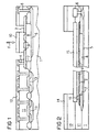
- a doped region 5 is formed in a substrate 1, preferably made of silicon.
- a Membrane 2 is located on a spacer layer 7 in which a cavity 8 is formed.
- This cavity forms one Space between the doped region 5 and the membrane 2 and can e.g. B. be produced in that by in Membrane 2 produced etching openings 9, the material of the spacer layer 7, initially as an auxiliary layer or sacrificial layer is produced, is etched out. If this sacrificial layer from silicon oxide z. B. by local oxidation of the silicon surface (LOCOS) is produced as an etchant HF suitable in aqueous solution; plasma etching can also be applied become.
- LOC local oxidation of the silicon surface
- the etching openings 9 are provided with a sealing layer locked.
- the production is simplified in that, as such, the planarization layer 11 is also used for covering the electronic components is used.
- BPSG borophosphosilicate glass
- MOSFETs 13 shown as components that are complementary MOSFETs manufactured as part of the CMOS process can be. It is therefore possible to use the invention Ultrasonic transducer completely together with all for the control electronics to integrate the required components.
- the electrical connection is made by vertical conductive Connections present in the planarization layer 11 are. These conductors are e.g. B. made by vias be etched and these contact holes with suitable Metal to be replenished. On top of layer 11 becomes a first metallization level, possibly in the same process step with the contact hole filling, applied and structured. Further intermediate oxide layers 12 can then be used applied to multiple levels of metallization realize.
- the membrane is made of doped polysilicon z. B. together with the polysilicon strips, which act as gate electrodes of the transistors are provided can. This doped polysilicon of membrane 2 is included provided a connection contact 4.
- the doped region 5 is provided as a counter electrode to the membrane with a contact 6.
- a remaining portion of the planarization layer 11 and further layers deposited thereon is in this embodiment leave on membrane 2 as stamp 10 Service.
- the etching openings 9 are closed with this stamp and at the same time stiffens the membrane 2.
- the thickness of this stamp can vary depending on the concerned Requirements.
- the thickness of the membrane that functions when the transducer is in operation Layer or layer sequence is in preferred embodiments typically about 0.5 ⁇ m to 5 ⁇ m, which in detail from using an additional stiffener Membrane, such as B. the stamp 10 depends.
- the one for the Membranes used for sound transducers can be different Have shapes (e.g. square, rectangular, hexagonal, octagonal, round). Typical dimensions are in the range of 20 to 200 ⁇ m (largest extension of that for sound radiation intended portion of the membrane layer).
- FIG 2 an embodiment is shown in which in addition to the substrate 1, the membrane 2, the doped Area 5, the contact 6 applied thereon, the spacer layer 7, the cavity 8, the etching openings 9, the planarization layer 11, and the intermediate oxide 12 a passivation layer 14 on the top, a top layer 15, the z. B. can consist of aluminum, over the membrane and a Terminal contact 16, the membrane 2 and the cover layer 15th connects with each other, drawn.
- the membrane 2 can be made very thin be, while at the same time sufficient mechanical stability and rigidity of the membrane by the applied Cover layer 15 is effected.
- the cover layer 15 can directly be applied to the membrane 2 or, as shown, on the lower planarization layer 11. The cover layer 15 is then z. B.
- the top layer can So part of the first level of metallization, for the Structuring of conductor tracks is used. If the doped region for the capacitive operation of the converter 5 and a conductive cover layer 15 (z. B. of metal) used the membrane 2 does not need to be electrically conductive to be, and the contact 16 can be omitted. In the embodiment 2, the cover layer is made of aluminum directly connected to the first conductor track level and the Contact 16 omitted.
- the ultrasonic transducer according to the invention as a single component in an array, i.e. H. an arrangement of a #1 of such individual components to be provided.
- Such an arrangement is shown in cross section in FIG. 3.
- the radiation areas of the Single transducers 31 are shown square there.
- the radiation areas the membranes of the single transducers can take place which have a different geometric shape, e.g. B. one of the above geometric shapes.
- a particularly suitable one Embodiment of the array sees a hexagonal grid and regular hexagons as radiation surfaces.
- the radiation areas do not all have to be the same, but can have different shapes and sizes. Laterally to the grid-shaped arrangement is in the illustrated Example an area 32 for electronic components is provided. It is advantageous if in the Spaces between the individual transducers 31 electronic Components are arranged around the electrical connections between the single transducers and the electronic components to shorten and simplify.
- the arrangement as a grid in particular need not be periodic, it So there is no need for a single converter at every point on the grid to be present.
- An arrangement made up of a variety of single converters and that has no periodicity can be advantageous for certain applications.
- the transducers can e.g. B. via one with the electronic circuit integrated multiplexer arrangement individually or in groups to one or more entrances or Outputs of the control circuit can be connected. Such alternating connection is best done through electronic Switches z. B. formed by complementary MOSFETs are realized.
- These sub-arrays can be fixed in a parent grid be set, or the selection of the partial arrays takes place sliding by adding to one side of the selected subset of individual converters the converters are deactivated, i.e. switched off and on the other hand a row or column of Single converters is switched on.
- Pseudo-random transducer arrangements offer additional advantages, so-called random arrays. You can use this comparatively fewer single-converter directional diagrams generated which are a pronounced main maximum and very low Show secondary maxima. Such a transducer arrangement receives one z. B. in that the transducers are arranged in a grid and individual grid points that are pseudo-random Selection criteria are determined, omitted. You can then fill in the gaps in the grid electronic components can be arranged. An irregular one Distribution of the single converter can also be used to Single transducers with different sizes and shapes of the radiation surfaces provided.
- An embodiment of an array according to the invention can z. B. provide a square array of 100x100 arrays in 10x10 square arrangements of 10x10 individual converters each to divide. These partial arrays of 100 each Single converters can then independently of one another simultaneously be activated, or it is possible in each of these sub-arrays a smooth control of z. B. 4 each in a square arranged single converters to make. Instead there is no need for a fixed division of the grid. For certain applications it can be advantageous if a Partial grid from z. B. 100 individual transducers arranged in a square is activated, in which case an outer Row or column of this array switched off and at the another side or another row or column of 10 single converters be connected to the sub-array.
- phased arrays With line-by-line and column-by-line control of individual converters or small sub-groups of single converters practically all applications of known Realize phased arrays.
- the principle of the phased array is based that several ultrasonic transducers are excited with signals be in their phase or in their temporal Position and / or be controlled in their amplitude.
- signals are e.g. B. in a direction of arrangement shifted from each other by a certain phase difference.
- the sound beam can be pivoted during transmission defined directional diagrams can be generated and the beam can be focused on certain spatial points become.
- the same options can also be calculated can be realized by superimposing the received signals. This is both a directivity in broadcast mode also a detection of the direction from which a sound wave hits, possible at reception.
- a suitable evaluation circuit therefore leaves the determination of all of that information to, which detects with ultrasound reception with such an array can be.
- the control of a converter arrangement operated as a phased array can be analog or digital using a shift register, the Z. B. very useful in the one shown in Figure 4, region 32 which is laterally adjacent to the actual array can be realized.
- a Shift registers for transmission mode, the transmission signal to the Input of the shift register created.
- the outputs of the Shift register cells are on rows or columns of Converters in the array.
- the single converter can on concentric rings around the center of symmetry of the arrangement horizontal single converters are operated in phase; the converters on rings further out run to the longer path length of the signals to a point above the center to compensate for the order. So that is the distance the focus of the emitted ultrasound is adjustable.
- Another improvement of the ultrasonic transducer according to the invention provides an improved operating circuit.
- a relatively high DC voltage than Bias between membrane and doped region 5 required.
- Bias between membrane and doped region 5 required.
- Such a bias increases sensitivity of the converter.
- Such a bias is preferably in the Range selected from 10 volts to 200 volts.
- a typical value with a membrane size of 50 ⁇ m to 100 ⁇ m is 100 volts.
- the sensitivity of the converter depends on various parameters from. The thickness and rigidity of the membrane are essential as well as the dimensions of the radiation area. On Gas trapped in the cavity 8 stiffens the membrane.
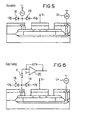
- FIGS. 5 and 6 show such special circuits for transmit mode and receive mode of the converter.
- a DC voltage U is applied between the connections of the membrane (or the conductive cover layer) and the doped region as a bias.
- the sensitivity of the converter improves with an increase in the electric field strength between the capacitor electrodes (between the membrane and the doped region in the described embodiment).
- the size of the maximum permissible field strength is limited by the physical properties of the materials used or the maximum deflection allowed.
- the purpose of the bias is to achieve the largest possible electromechanical coupling factor and thus the highest possible sensitivity of the converter.
- the coupling factor reaches its greatest value one when the membrane is deflected by the bias voltage up to the unstable point caused by the nonlinear electrostatic effect.
- the maximum value of the deflection caused by a prestress is 33% in the case of a coplanar deflection of the membrane (plate capacitor with variable plate spacing) and correspondingly higher in the case of the membranes of the transducer according to the invention, which are arched when deflected.
- Good efficiencies with stable working behavior in operation result from static deflections of 1% to 20% due to the preload.
- the AC voltage U - provided for the transmission mode is applied to one of the two connections, in the example of FIG. 5 the connection of the membrane.
- Figure 6 shows a corresponding circuit for receiving operation.
- the AC voltage to be connected is replaced there by a suitable transistor preamplifier circuit, which is symbolized in FIG. 6 by an operational amplifier circuit 20.
- the circuit is designed as low-impedance as a current amplifier on the input side.
- it can also be expedient to set the input resistance R of the circuit in connection with the value of the direct voltage U in such a way that the mechanical component is optimally damped.
- the DC voltage for receiving operation is preferably also between 10 volts and 200 volts.
- the DC voltage is chosen so high that a predetermined maximum deflection of the membrane causes at least one intended change in the value of this DC voltage and / or an electrical current produced with at least one intended current intensity.
Landscapes
- Physics & Mathematics (AREA)
- General Physics & Mathematics (AREA)
- Transducers For Ultrasonic Waves (AREA)
- Measurement Of Velocity Or Position Using Acoustic Or Ultrasonic Waves (AREA)
- Measurement Of Mechanical Vibrations Or Ultrasonic Waves (AREA)
- Investigating Or Analyzing Materials By The Use Of Ultrasonic Waves (AREA)
- Ultra Sonic Daignosis Equipment (AREA)
Claims (21)
- Transducteur à ultrasons sur un substrat (1),dans lequel il est formé dans le substrat une zone (5) dopée,dans lequel il est disposé une membrane (2) micromécanique sur une couche (7) intercalaire à distance de cette zone,dans lequel il y a, entre la zone dopée et la membrane, une cavité (8) qui permet une excursion maximum prévue de la membrane par rapport au substrat,dans lequel la membrane est conductrice de l'électricité ou est reliée mécaniquement à une couche (15) conductrice de l'électricité disposée dans la zone de la surface de la membrane,dans lequel la membrane ou la couche conductrice de l'électricité qui y est reliée et la zone dopée sont munies respectivement chacune d'un contact (4, 6) formant borne,dans lequel des composants électroniques sont intégrés sur le substrat etdans lequel ces composants sont reliés entre eux et aux contacts formant bornes de façon à former un circuit de commande par lequel il est possible d'exciter la membrane pour qu'elle effectue des oscillations d'ultrasons ou de détecter des oscillations d'ultrasons de la membrane qui sont présentes.
- Transducteur à ultrasons suivant la revendication 1, dans lequel la membrane est en silicium ou en polysilicium ou a une proportion de couche en silicium ou en polysilicium.
- Transducteur à ultrasons suivant la revendication 1 ou 2, dans lequel la membrane est munie, au moins sur l'une des faces prévues pour le fonctionnement du transducteur à ultrasons, d'une couche (15) de finition en un matériau autre que du silicium.
- Transducteur à ultrasons suivant l'une des revendications 1 à 3, dans lequel il y a un couronnement (10) en forme de poinçon dans une partie médiane de la surface de la membrane qui est prévue pour le fonctionnement du transducteur à ultrasons.
- Transducteur à ultrasons suivant l'une des revendications 1 à 4, dans lequel il est prévu, comme composants électroniques, des MOSFET complémentaires ou/et des transistors bipolaires.
- Transducteur à ultrasons suivant l'une des revendications 1 à 5, dans lequel le circuit de commande est conçu pour le fonctionnement en émission et il est prévu, à cet effet, d'appliquer aux contacts (4, 6) formant borne une tension (U=) continue et une tension (U∼) alternative prévue pour l'excitation d'une oscillation ultrasonore et
dans lequel la tension (U=) continue est choisie si haute qu'une amplitude prévue de la tension (U∼) alternative provoque au moins une amplitude prévue de l'oscillation de la membrane. - Transducteur à ultrasons suivant l'une des revendications 1 à 5, dans lequel le circuit de commande est conçu pour un fonctionnement en réception et il est prévu à cet effet d'appliquer aux contacts (4, 6) formant borne une tension (U=) continue qui est choisie si haut qu'une excursion maximum donnée à l'avance de la membrane provoque au moins une modification prévue de la valeur de cette tension continue et/ou un courant électrique provoqué ayant au moins une intensité de courant prévue et
dans lequel un contact (4) formant borne est relié à une partie prévue comme amplificateur (20) du circuit de commande. - Transducteur à ultrasons suivant la revendication 7, dans lequel la résistance (R) d'entrée de l'amplificateur (20) est réglée de façon à donner une largeur de bande prévue du récepteur.
- Transducteur à ultrasons suivant l'une des revendications 1 à 8, dans lequel un contact formant borne est relié par des diodes (18, 19) à des potentiels de fonctionnement d'une tension d'alimentation, de façon qu'un potentiel appliqué à ce contact formant borne, qui se trouve en dehors de l'intervalle délimité par ces potentiels de fonctionnement, soit court-circuité vers l'un des potentiels de fonctionnement.
- Transducteur à ultrasons suivant l'une des revendications 1 à 9, dans lequel le circuit de commande est conçu pour un fonctionnement en alternance en émission et en réception en tant que multiplexeur et
dans lequel un interrupteur fait partie du circuit de commande et permet une commutation entre le fonctionnement en émission et le fonctionnement en réception. - Agencement de plusieurs transducteurs à ultrasons suivant l'une des revendications 1 à 10 sur le même substrat,
dans lequel les circuits de commande sont établis de façon à brancher les transducteurs à ultrasons entre eux de manière coordonnée en fonctionnement en émission et en fonctionnement en réception. - Agencement suivant la revendication 11, dans lequel les circuits de commande sont établis de manière à mettre en fonctionnement ou hors de fonctionnement les transducteurs à ultrasons individuellement ou en groupe suivant une succession dans le temps qui peut être donné à l'avance.
- Agencement suivant la revendication 11 ou 12, dans lequel l'ensemble des transducteurs à ultrasons présents est réparti d'une manière fixe en groupes de transducteurs à ultrasons et
dans lequel les circuits de commande sont établis de façon à mettre en fonctionnement ou hors de fonctionnement simultanément les transducteurs à ultrasons de chaque groupe. - Agencement suivant la revendication 11 ou 12,
dans lequel les circuits de commande sont établis de manière à mettre en fonctionnement un groupe variable dans le temps parmi la totalité des transducteurs à ultrasons, ces groupes pouvant être modifiés de manière à mettre hors de fonctionnement à des intervalles de temps donnés à l'avance une proportion des transducteurs à ultrasons mis en fonctionnement et à mettre en fonctionnement un certain nombre d'autres transducteurs à ultrasons. - Agencement suivant la revendication 11,
dans lequel les circuits de commande sont établis pour faire fonctionner les transducteurs à ultrasons en émission de façon à ce que, par les phases relatives ou les successions dans le temps des signaux à envoyer aux divers transducteurs à ultrasons, il est provoqué un effet directif de l'ultrason émis. - Agencement suivant la revendication 11,
dans lequel les circuits de commande sont établis pour faire fonctionner les ultrasons en mode de réception de façon à ce que, par une superposition par le calcul des phases relatives ou des successions dans le temps des signaux reçus par divers transducteurs à ultrasons, il est provoqué une reconnaissance de la direction de l'ultrason reçu. - Agencement suivant la revendication 15 ou 16,
dans lequel les circuits de commande comprennent au moins un registre à décalage. - Agencement suivant l'une des revendications 11 à 17,
dans lequel les transducteurs à ultrasons sont disposés dans une trame plane périodique au moins dans une direction et emplissent cette trame. - Agencement suivant l'une des revendications 13 à 14,
dans lequel les transducteurs à ultrasons sont disposés dans une trame plane périodique au moins dans une direction et
dans lequel les groupes de transducteurs à ultrasons qui sont mis respectivement en fonctionnement en commun emplissent une partie respective de la trame. - Agencement suivant l'une des revendications 11 à 17,
dans lequel les transducteurs à ultrasons sont disposés suivant des carrés ou des hexagones réguliers qui forment un parquetage sans discontinuité du plan et
dans lequel les surfaces des membranes qui sont prévues pour le fonctionnement des transducteurs à ultrasons sont respectivement des carrés ou des hexagones. - Agencement suivant l'une des revendications 11 à 17,
dans lequel les transducteurs à ultrasons sont disposés de manière à éviter dans chaque direction une périodicité de l'agencement.
Applications Claiming Priority (3)
| Application Number | Priority Date | Filing Date | Title |
|---|---|---|---|
| DE19643893 | 1996-10-30 | ||
| DE19643893A DE19643893A1 (de) | 1996-10-30 | 1996-10-30 | Ultraschallwandler in Oberflächen-Mikromechanik |
| PCT/DE1997/002505 WO1998019140A2 (fr) | 1996-10-30 | 1997-10-28 | Transducteur a ultrasons realise selon une technique de micro-usinage de surface |
Publications (2)
| Publication Number | Publication Date |
|---|---|
| EP0935741A2 EP0935741A2 (fr) | 1999-08-18 |
| EP0935741B1 true EP0935741B1 (fr) | 2003-07-23 |
Family
ID=7809662
Family Applications (1)
| Application Number | Title | Priority Date | Filing Date |
|---|---|---|---|
| EP97949856A Expired - Lifetime EP0935741B1 (fr) | 1996-10-30 | 1997-10-28 | Transducteur a ultrasons realise selon une technique de micro-usinage de surface avec circuit de controle integre, et matrice |
Country Status (5)
| Country | Link |
|---|---|
| US (1) | US6320239B1 (fr) |
| EP (1) | EP0935741B1 (fr) |
| JP (1) | JP3395844B2 (fr) |
| DE (2) | DE19643893A1 (fr) |
| WO (1) | WO1998019140A2 (fr) |
Families Citing this family (66)
| Publication number | Priority date | Publication date | Assignee | Title |
|---|---|---|---|---|
| DE19829609B4 (de) * | 1998-07-02 | 2008-04-30 | Robert Bosch Gmbh | Verfahren zur Herstellung eines Mikrosystems |
| DE19839606C1 (de) * | 1998-08-31 | 2000-04-27 | Siemens Ag | Mikromechanisches Bauelement und Verfahren zu dessen Herstellung |
| DE19845537A1 (de) * | 1998-10-02 | 2000-04-13 | Grundfos A S Bjerringbro | Sensor und Verfahren zu seiner Herstellung |
| DE19922967C2 (de) * | 1999-05-19 | 2001-05-03 | Siemens Ag | Mikromechanischer kapazitiver Ultraschallwandler und Verfahren zu dessen Herstellung |
| US6246158B1 (en) | 1999-06-24 | 2001-06-12 | Sensant Corporation | Microfabricated transducers formed over other circuit components on an integrated circuit chip and methods for making the same |
| DE10104868A1 (de) | 2001-02-03 | 2002-08-22 | Bosch Gmbh Robert | Mikromechanisches Bauelement sowie ein Verfahren zur Herstellung eines mikromechanischen Bauelements |
| US6552404B1 (en) * | 2001-04-17 | 2003-04-22 | Analog Devices, Inc. | Integratable transducer structure |
| DE10122765A1 (de) * | 2001-05-10 | 2002-12-05 | Campus Micro Technologies Gmbh | Elektroakustischer Wandler zur Erzeugung oder Erfassung von Ultraschall, Wandler-Array und Verfahren zur Herstellung der Wandler bzw. der Wandler-Arrays |
| US6659954B2 (en) * | 2001-12-19 | 2003-12-09 | Koninklijke Philips Electronics Nv | Micromachined ultrasound transducer and method for fabricating same |
| US7443765B2 (en) * | 2003-03-06 | 2008-10-28 | General Electric Company | Reconfigurable linear sensor arrays for reduced channel count |
| US6865140B2 (en) * | 2003-03-06 | 2005-03-08 | General Electric Company | Mosaic arrays using micromachined ultrasound transducers |
| US7257051B2 (en) * | 2003-03-06 | 2007-08-14 | General Electric Company | Integrated interface electronics for reconfigurable sensor array |
| US7353056B2 (en) * | 2003-03-06 | 2008-04-01 | General Electric Company | Optimized switching configurations for reconfigurable arrays of sensor elements |
| US7313053B2 (en) * | 2003-03-06 | 2007-12-25 | General Electric Company | Method and apparatus for controlling scanning of mosaic sensor array |
| US7280435B2 (en) * | 2003-03-06 | 2007-10-09 | General Electric Company | Switching circuitry for reconfigurable arrays of sensor elements |
| DE10325406B4 (de) * | 2003-06-05 | 2005-04-28 | Eads Deutschland Gmbh | Schadensermittlung an zu prüfenden Strukturen mittels Ultraschall |
| TWI240990B (en) * | 2003-10-21 | 2005-10-01 | Ind Tech Res Inst | Preparation method of micromachined capacitive ultrasonic transducer by the imprinting technique |
| US20050121734A1 (en) * | 2003-11-07 | 2005-06-09 | Georgia Tech Research Corporation | Combination catheter devices, methods, and systems |
| US7030536B2 (en) * | 2003-12-29 | 2006-04-18 | General Electric Company | Micromachined ultrasonic transducer cells having compliant support structure |
| US7052464B2 (en) * | 2004-01-01 | 2006-05-30 | General Electric Company | Alignment method for fabrication of integrated ultrasonic transducer array |
| EP1713399A4 (fr) * | 2004-02-06 | 2010-08-11 | Georgia Tech Res Inst | Dispositifs cmut et procedes de fabrication |
| WO2005084284A2 (fr) * | 2004-02-27 | 2005-09-15 | Georgia Tech Research Corporation | Dispositifs cmut a elements electrodes multiples, et procedes de fabrication |
| US7646133B2 (en) * | 2004-02-27 | 2010-01-12 | Georgia Tech Research Corporation | Asymmetric membrane cMUT devices and fabrication methods |
| WO2005084267A2 (fr) * | 2004-02-27 | 2005-09-15 | Georgia Tech Research Corporation | Dispositifs cmut et leurs procedes de fabrication |
| WO2005114820A2 (fr) * | 2004-05-14 | 2005-12-01 | The University Of Georgia Research Foundation, Inc. | Systemes et procedes de transducteurs ultrasonores pouvant etre implantes |
| US7888709B2 (en) * | 2004-09-15 | 2011-02-15 | Sonetics Ultrasound, Inc. | Capacitive micromachined ultrasonic transducer and manufacturing method |
| US8658453B2 (en) * | 2004-09-15 | 2014-02-25 | Sonetics Ultrasound, Inc. | Capacitive micromachined ultrasonic transducer |
| US8309428B2 (en) * | 2004-09-15 | 2012-11-13 | Sonetics Ultrasound, Inc. | Capacitive micromachined ultrasonic transducer |
| JP4471856B2 (ja) * | 2005-01-27 | 2010-06-02 | 株式会社日立製作所 | 超音波トランスデューサおよびその製造方法 |
| US7589456B2 (en) * | 2005-06-14 | 2009-09-15 | Siemens Medical Solutions Usa, Inc. | Digital capacitive membrane transducer |
| JP4523879B2 (ja) * | 2005-06-20 | 2010-08-11 | 株式会社日立製作所 | 電気・音響変換素子、アレイ型超音波トランスデューサおよび超音波診断装置 |
| US20070038088A1 (en) * | 2005-08-04 | 2007-02-15 | Rich Collin A | Medical imaging user interface and control scheme |
| JP4724501B2 (ja) * | 2005-09-06 | 2011-07-13 | 株式会社日立製作所 | 超音波トランスデューサおよびその製造方法 |
| DE102005050159A1 (de) * | 2005-10-19 | 2007-04-26 | Siemens Ag | Schwingungssensor |
| US20070142699A1 (en) * | 2005-12-16 | 2007-06-21 | Acoustx Corporation | Methods and implantable apparatuses for treating an esophageal disorder such as gastroesophageal reflux disease |
| US20070142884A1 (en) * | 2005-12-16 | 2007-06-21 | Acoustx Corporation | Methods and apparatuses for treating an esophageal disorder such as gastroesophageal reflux disease |
| JP4787648B2 (ja) * | 2006-03-29 | 2011-10-05 | パナソニック株式会社 | コンデンサマイクロホンの製造方法およびコンデンサマイクロホン |
| JP4699259B2 (ja) * | 2006-03-31 | 2011-06-08 | 株式会社日立製作所 | 超音波トランスデューサ |
| JP4979283B2 (ja) * | 2006-06-29 | 2012-07-18 | 株式会社日立製作所 | 半導体装置の製造方法および半導体装置 |
| JP4972350B2 (ja) * | 2006-06-30 | 2012-07-11 | 株式会社日立製作所 | 半導体装置の製造方法 |
| JP4952164B2 (ja) * | 2006-09-20 | 2012-06-13 | 株式会社デンソー | 流量計測素子、質量流量計 |
| JP5016884B2 (ja) * | 2006-09-29 | 2012-09-05 | 株式会社日立製作所 | 半導体装置およびその製造方法 |
| US7745248B2 (en) * | 2007-10-18 | 2010-06-29 | The Board Of Trustees Of The Leland Stanford Junior University | Fabrication of capacitive micromachined ultrasonic transducers by local oxidation |
| JP5016449B2 (ja) * | 2007-11-13 | 2012-09-05 | ローム株式会社 | 半導体装置 |
| JP2010004199A (ja) * | 2008-06-19 | 2010-01-07 | Hitachi Ltd | 超音波トランスデューサおよびその製造方法 |
| CN102149429B (zh) | 2008-07-10 | 2016-10-12 | 康奈尔大学 | 产生超声波的装置 |
| JP5851238B6 (ja) | 2009-03-05 | 2023-12-15 | 株式会社日立メディコ | 超音波トランスデューサ、その製造方法、および、それを用いた超音波探触子 |
| US8315125B2 (en) * | 2009-03-18 | 2012-11-20 | Sonetics Ultrasound, Inc. | System and method for biasing CMUT elements |
| CN102440005B (zh) | 2009-05-25 | 2014-09-24 | 株式会社日立医疗器械 | 超声波换能器及利用该超声波换能器的超声波诊断装置 |
| US7888844B2 (en) * | 2009-06-30 | 2011-02-15 | Avago Technologies Wireless Ip (Singapore) Pte. Ltd. | Temperature control of micromachined transducers |
| US8897470B2 (en) * | 2009-07-31 | 2014-11-25 | Macronix International Co., Ltd. | Method of fabricating integrated semiconductor device with MOS, NPN BJT, LDMOS, pre-amplifier and MEMS unit |
| JP5414546B2 (ja) * | 2010-01-12 | 2014-02-12 | キヤノン株式会社 | 容量検出型の電気機械変換素子 |
| JP5355777B2 (ja) | 2010-03-12 | 2013-11-27 | 株式会社日立メディコ | 超音波トランスデューサおよびそれを用いた超音波診断装置 |
| US8357981B2 (en) | 2010-05-28 | 2013-01-22 | Avago Technologies Wireless Ip (Singapore) Pte. Ltd. | Transducer devices having different frequencies based on layer thicknesses and method of fabricating the same |
| JP5178791B2 (ja) * | 2010-08-23 | 2013-04-10 | オリンパス株式会社 | 静電容量型超音波振動子 |
| US9608589B2 (en) | 2010-10-26 | 2017-03-28 | Avago Technologies General Ip (Singapore) Pte. Ltd. | Method of forming acoustic resonator using intervening seed layer |
| CA2873394A1 (fr) * | 2012-05-11 | 2013-11-14 | Volcano Corporation | Architectures de circuit et interfaces electriques pour dispositifs ultrasonores intravasculaires (ivus) rotatifs |
| JP6189033B2 (ja) | 2012-12-14 | 2017-08-30 | 株式会社日立製作所 | 超音波探触子の製造方法、超音波探触子、及び超音波診断装置 |
| KR102207928B1 (ko) | 2014-08-13 | 2021-01-26 | 삼성전자주식회사 | 음향 센싱 소자 및 주파수 정보 획득 방법 |
| JP6251661B2 (ja) * | 2014-09-26 | 2017-12-20 | 株式会社日立製作所 | 超音波トランスデューサ、その製造方法、超音波トランスデューサアレイ及び超音波検査装置 |
| US11147531B2 (en) | 2015-08-12 | 2021-10-19 | Sonetics Ultrasound, Inc. | Method and system for measuring blood pressure using ultrasound by emitting push pulse to a blood vessel |
| WO2018237267A1 (fr) * | 2017-06-23 | 2018-12-27 | Butterfly Network, Inc. | Élément de transducteur à ultrasons différentiel pour dispositifs à ultrasons |
| US10966683B2 (en) | 2018-03-22 | 2021-04-06 | Exo Imaging Inc. | Integrated ultrasonic transducers |
| US12099150B2 (en) | 2021-10-26 | 2024-09-24 | Exo Imaging, Inc. | Multi-transducer chip ultrasound device |
| EP4580505A1 (fr) * | 2022-09-02 | 2025-07-09 | Exo Imaging Inc. | Transducteurs ultrasonores micro-usinés à membranes doubles et multiples |
| US12533711B2 (en) | 2022-09-02 | 2026-01-27 | Exo Imaging, Inc. | Dual and multiple membrane micromachined ultrasound transducers |
Family Cites Families (5)
| Publication number | Priority date | Publication date | Assignee | Title |
|---|---|---|---|---|
| JPS5938621A (ja) | 1982-08-27 | 1984-03-02 | Nissan Motor Co Ltd | 振動分析装置 |
| US4699009A (en) | 1985-11-05 | 1987-10-13 | Acuson | Dynamically focused linear phased array acoustic imaging system |
| US4873871A (en) | 1988-06-17 | 1989-10-17 | Motorola, Inc. | Mechanical field effect transistor sensor |
| DE4318466B4 (de) | 1993-06-03 | 2004-12-09 | Robert Bosch Gmbh | Verfahren zur Herstellung eines mikromechanischen Sensors |
| ATE178142T1 (de) * | 1994-01-18 | 1999-04-15 | Siemens Ag | Verfahren zur herstellung eines beschleunigungssensors |
-
1996
- 1996-10-30 DE DE19643893A patent/DE19643893A1/de not_active Withdrawn
-
1997
- 1997-10-28 US US09/297,243 patent/US6320239B1/en not_active Expired - Fee Related
- 1997-10-28 EP EP97949856A patent/EP0935741B1/fr not_active Expired - Lifetime
- 1997-10-28 JP JP51990398A patent/JP3395844B2/ja not_active Expired - Fee Related
- 1997-10-28 WO PCT/DE1997/002505 patent/WO1998019140A2/fr not_active Ceased
- 1997-10-28 DE DE59710477T patent/DE59710477D1/de not_active Expired - Fee Related
Also Published As
| Publication number | Publication date |
|---|---|
| US6320239B1 (en) | 2001-11-20 |
| JP2001502871A (ja) | 2001-02-27 |
| DE19643893A1 (de) | 1998-05-07 |
| WO1998019140A3 (fr) | 1998-07-09 |
| EP0935741A2 (fr) | 1999-08-18 |
| DE59710477D1 (de) | 2003-08-28 |
| WO1998019140A2 (fr) | 1998-05-07 |
| JP3395844B2 (ja) | 2003-04-14 |
Similar Documents
| Publication | Publication Date | Title |
|---|---|---|
| EP0935741B1 (fr) | Transducteur a ultrasons realise selon une technique de micro-usinage de surface avec circuit de controle integre, et matrice | |
| DE60215512T2 (de) | Mikrobearbeitete Ultraschallwandleranordnung | |
| DE602005006419T2 (de) | Elektroakustischer Wandler für Hochfrequenzanwendungen | |
| EP0025092B1 (fr) | Transducteur ultrasonore et procédé pour sa fabrication | |
| DE102004011193A1 (de) | Mosaikarrayanordnung, die mikrobearbeitete Ultraschalltransducer nutzt | |
| US20040251784A1 (en) | Laminated structure and method of manufacturing the same | |
| DE19701334A1 (de) | Mit der zweiten Harmonischen abbildende Wandler | |
| DE19735155A1 (de) | Beschleunigungssensor | |
| DE10341730B4 (de) | Vielseitige Transducer-Array-Konfigurationen | |
| DE102019220132B4 (de) | Piezoelektrisches Element und Verfahren zum Herstellen eines piezoelektrischen Elements | |
| WO2007038914A1 (fr) | Transformateur piezo-electrique et procede de fabrication associe | |
| DE69926487T2 (de) | Akustisches element | |
| WO2011073414A2 (fr) | Ensemble oscillant pour transducteur ultrasonore et procédé de fabrication de cet ensemble oscillant | |
| DE102005008514B4 (de) | Mikrofonmembran und Mikrofon mit der Mikrofonmembran | |
| EP2001604A2 (fr) | Convertisseur électroacoustique | |
| EP1497869A2 (fr) | Composant a semi-conducteur dans lequel est integree une structure de condensateur comprenant une pluralite de couches de metallisation | |
| JPH0886777A (ja) | 超音波探針器 | |
| EP0825585B1 (fr) | Dispositif pour la détermination de distances à objets | |
| EP3386649A1 (fr) | Ensemble transducteur acoustique comprenant une couche métallique structurée et procédé de fabrication d'un ensemble transducteur acoustique comprenant une couche métallique structurée | |
| EP0160821B1 (fr) | Dispositif de lecture d'une image de charges bidimensionnelle au moyen d'une barrette de capteurs | |
| WO2002066267A2 (fr) | Transducteur piezo-electrique utilise pour produire des ultrasons | |
| DE4115221C2 (de) | Elektroakustischer Wandler nach dem elektrostatischen Prinzip | |
| EP3386650B1 (fr) | Ensemble transducteur acoustique comprenant deux éléments de jonction disposés parallèlement et procédé de fabrication d'un ensemble transducteur acoustique comprenant deux éléments de jonction disposés parallèlement | |
| DE102012216996A1 (de) | MEMS-Schallwandler, MEMS-Schallwandleranordnung und Verfahren zum Herstellen eines MEMS-Schallwandlers | |
| DE102024204501A1 (de) | Mikro-elektro-mechanisches Schwingungssystem |
Legal Events
| Date | Code | Title | Description |
|---|---|---|---|
| PUAI | Public reference made under article 153(3) epc to a published international application that has entered the european phase |
Free format text: ORIGINAL CODE: 0009012 |
|
| 17P | Request for examination filed |
Effective date: 19990419 |
|
| AK | Designated contracting states |
Kind code of ref document: A2 Designated state(s): CH DE FR GB LI |
|
| 17Q | First examination report despatched |
Effective date: 20010326 |
|
| RAP1 | Party data changed (applicant data changed or rights of an application transferred) |
Owner name: INFINEON TECHNOLOGIES AG |
|
| GRAH | Despatch of communication of intention to grant a patent |
Free format text: ORIGINAL CODE: EPIDOS IGRA |
|
| RTI1 | Title (correction) |
Free format text: SURFACE MICRO-MECHANIC ULTRASONIC TRANSDUCER WITH INTEGRATED CONTROL CIRCUIT, AND ARRAY |
|
| GRAH | Despatch of communication of intention to grant a patent |
Free format text: ORIGINAL CODE: EPIDOS IGRA |
|
| GRAA | (expected) grant |
Free format text: ORIGINAL CODE: 0009210 |
|
| AK | Designated contracting states |
Designated state(s): CH DE FR GB LI |
|
| REG | Reference to a national code |
Ref country code: GB Ref legal event code: FG4D Free format text: NOT ENGLISH |
|
| REG | Reference to a national code |
Ref country code: CH Ref legal event code: EP |
|
| REF | Corresponds to: |
Ref document number: 59710477 Country of ref document: DE Date of ref document: 20030828 Kind code of ref document: P |
|
| REG | Reference to a national code |
Ref country code: CH Ref legal event code: NV Representative=s name: ICB INGENIEURS CONSEILS EN BREVETS SA |
|
| GBT | Gb: translation of ep patent filed (gb section 77(6)(a)/1977) |
Effective date: 20031103 |
|
| ET | Fr: translation filed | ||
| PLBE | No opposition filed within time limit |
Free format text: ORIGINAL CODE: 0009261 |
|
| STAA | Information on the status of an ep patent application or granted ep patent |
Free format text: STATUS: NO OPPOSITION FILED WITHIN TIME LIMIT |
|
| 26N | No opposition filed |
Effective date: 20040426 |
|
| PGFP | Annual fee paid to national office [announced via postgrant information from national office to epo] |
Ref country code: CH Payment date: 20061012 Year of fee payment: 10 |
|
| PGFP | Annual fee paid to national office [announced via postgrant information from national office to epo] |
Ref country code: GB Payment date: 20061023 Year of fee payment: 10 |
|
| PGFP | Annual fee paid to national office [announced via postgrant information from national office to epo] |
Ref country code: DE Payment date: 20061212 Year of fee payment: 10 |
|
| GBPC | Gb: european patent ceased through non-payment of renewal fee |
Effective date: 20071028 |
|
| REG | Reference to a national code |
Ref country code: CH Ref legal event code: PL |
|
| PG25 | Lapsed in a contracting state [announced via postgrant information from national office to epo] |
Ref country code: LI Free format text: LAPSE BECAUSE OF NON-PAYMENT OF DUE FEES Effective date: 20071031 Ref country code: DE Free format text: LAPSE BECAUSE OF NON-PAYMENT OF DUE FEES Effective date: 20080501 Ref country code: CH Free format text: LAPSE BECAUSE OF NON-PAYMENT OF DUE FEES Effective date: 20071031 |
|
| REG | Reference to a national code |
Ref country code: FR Ref legal event code: ST Effective date: 20080630 |
|
| PGFP | Annual fee paid to national office [announced via postgrant information from national office to epo] |
Ref country code: FR Payment date: 20061016 Year of fee payment: 10 |
|
| PG25 | Lapsed in a contracting state [announced via postgrant information from national office to epo] |
Ref country code: GB Free format text: LAPSE BECAUSE OF NON-PAYMENT OF DUE FEES Effective date: 20071028 |
|
| PG25 | Lapsed in a contracting state [announced via postgrant information from national office to epo] |
Ref country code: FR Free format text: LAPSE BECAUSE OF NON-PAYMENT OF DUE FEES Effective date: 20071031 |