EP0936494A2 - Dispositif d'affichage à cristal liquide muni d' une matrice noire multicouche SiOxNy - Google Patents
Dispositif d'affichage à cristal liquide muni d' une matrice noire multicouche SiOxNy Download PDFInfo
- Publication number
- EP0936494A2 EP0936494A2 EP99102422A EP99102422A EP0936494A2 EP 0936494 A2 EP0936494 A2 EP 0936494A2 EP 99102422 A EP99102422 A EP 99102422A EP 99102422 A EP99102422 A EP 99102422A EP 0936494 A2 EP0936494 A2 EP 0936494A2
- Authority
- EP
- European Patent Office
- Prior art keywords
- layer
- black matrix
- sio
- layers
- substrate
- Prior art date
- Legal status (The legal status is an assumption and is not a legal conclusion. Google has not performed a legal analysis and makes no representation as to the accuracy of the status listed.)
- Granted
Links
Images


Classifications
-
- G—PHYSICS
- G02—OPTICS
- G02F—OPTICAL DEVICES OR ARRANGEMENTS FOR THE CONTROL OF LIGHT BY MODIFICATION OF THE OPTICAL PROPERTIES OF THE MEDIA OF THE ELEMENTS INVOLVED THEREIN; NON-LINEAR OPTICS; FREQUENCY-CHANGING OF LIGHT; OPTICAL LOGIC ELEMENTS; OPTICAL ANALOGUE/DIGITAL CONVERTERS
- G02F1/00—Devices or arrangements for the control of the intensity, colour, phase, polarisation or direction of light arriving from an independent light source, e.g. switching, gating or modulating; Non-linear optics
- G02F1/01—Devices or arrangements for the control of the intensity, colour, phase, polarisation or direction of light arriving from an independent light source, e.g. switching, gating or modulating; Non-linear optics for the control of the intensity, phase, polarisation or colour
- G02F1/13—Devices or arrangements for the control of the intensity, colour, phase, polarisation or direction of light arriving from an independent light source, e.g. switching, gating or modulating; Non-linear optics for the control of the intensity, phase, polarisation or colour based on liquid crystals, e.g. single liquid crystal display cells
- G02F1/133—Constructional arrangements; Operation of liquid crystal cells; Circuit arrangements
- G02F1/1333—Constructional arrangements; Manufacturing methods
- G02F1/1335—Structural association of cells with optical devices, e.g. polarisers or reflectors
- G02F1/133509—Filters, e.g. light shielding masks
- G02F1/133512—Light shielding layers, e.g. black matrix
-
- G—PHYSICS
- G02—OPTICS
- G02F—OPTICAL DEVICES OR ARRANGEMENTS FOR THE CONTROL OF LIGHT BY MODIFICATION OF THE OPTICAL PROPERTIES OF THE MEDIA OF THE ELEMENTS INVOLVED THEREIN; NON-LINEAR OPTICS; FREQUENCY-CHANGING OF LIGHT; OPTICAL LOGIC ELEMENTS; OPTICAL ANALOGUE/DIGITAL CONVERTERS
- G02F1/00—Devices or arrangements for the control of the intensity, colour, phase, polarisation or direction of light arriving from an independent light source, e.g. switching, gating or modulating; Non-linear optics
- G02F1/01—Devices or arrangements for the control of the intensity, colour, phase, polarisation or direction of light arriving from an independent light source, e.g. switching, gating or modulating; Non-linear optics for the control of the intensity, phase, polarisation or colour
- G02F1/13—Devices or arrangements for the control of the intensity, colour, phase, polarisation or direction of light arriving from an independent light source, e.g. switching, gating or modulating; Non-linear optics for the control of the intensity, phase, polarisation or colour based on liquid crystals, e.g. single liquid crystal display cells
- G02F1/133—Constructional arrangements; Operation of liquid crystal cells; Circuit arrangements
- G02F1/1333—Constructional arrangements; Manufacturing methods
- G02F1/1335—Structural association of cells with optical devices, e.g. polarisers or reflectors
- G02F1/133502—Antiglare, refractive index matching layers
Definitions
- This application relates to a liquid crystal display (LCD) including a black matrix. More particulary, this application relates to a liquid crystal display including a multilayer black matrix portion that includes at least one layer of silicon oxynitride.
- LCDs Liquid crystal displays
- black matrices are known in the art.
- U. S. Patent Nos. 5,666,177; 5,682,211; and 5,641,974 the disclosures of which are hereby incorporated herein by reference.
- black matrices in LCDS are provided, and must be able to absorb and reflect light.
- Black matrices are often located on the color filter substrate and function to prevent ambient light surrounding the display from reducing display contrast, and to efficiently do this, reflection of light off of the black matrix must be kept to a minimum.
- materials have been conventionally used for black matrix applications, include CrO x and Cr combinations, black polymer, black polyimide, SiO x and Si combinations, and Si-rich SiN x
- Silicon dioxide has an index of refraction substantially matched (i.e. very close) to glass, however, its index does not substantially match with a-Si film which is typically used with silicon dioxide in black matric applications.
- PECVD silicon nitride typically has a refractive index between 1.8 and 2.2, and it thus does not always substantially match with glass (glass has a refractive index of about 1.5).
- Another object of this invention is to provide a multilayer black matrix, for use in display applications, that includes at least one silicon oxynitride layer (SiO x N y ).
- Another object of this invention is to provide a black matrix whose refractive index is adjustable or changeable at certain areas thereof between values of from about 1.5 and 4.5 by varying x and y of a layer(s), e.g. SiO x N y .
- a layer(s) e.g. SiO x N y
- This can be done, for example, by changing gas ratios of SiH 4 /NH 3 /N 2 O/H 2 /N 2 /O 2 (all of these gases or any combination thereof) in a PECVD deposition process and utilizing SiO x N y as a layer(s) in a black matrix system.
- Yet another object of this invention is to provide a multilayer black matrix with either abrupt interface (e.g. SiO x1 N y1 /SiO x2 N y2 / ..../SiO xn N yn ) or a gradual interface (e.g. SiO x(t) N y(t) ) that can be deposited.
- Abrupt interface multilayer black matrix systems can be deposited by turning off RF power while gas ratio(s) are changed, while a gradual interface black matrix layer system can be formed with RF power on while simultaneously changing gas ratio.
- SiO x N y are functions of time at certain layer locations, and in certain further embodiments each SiO x N y layer has at least one portion (near an interface with an adjacent layer) where "x" and/or "y" are functions of time and another portion (near the center of the layer) where "x" and/or "y" are substantially constant.
- this invention may fulfill the above described needs in the art by providing a liquid crystal display comprising:
- This invention further fulfills the above described needs in the art by providing a liquid crystal display comprising:
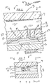
- FIG. 1 is a side cross sectional view of an LCD including black matrix system 3 according to an embodiment of this invention.
- the LCD includes substantially transparent active matrix substrate 5 (e.g. glass or plastic), substantially transparent passive or color filter substrate 7 (e.g. of glass or plastic), twisted nematic liquid crystal layer 8 sandwiched between the two substrates, and switching thin film transistors (TFTs) 9 provided on active substrate 5.
- the "active" substrate is the substrate which has the switching devices (e.g. TFTs 9 or diodes) provided thereon.
- Each TFT includes gate electrode 15, a-Si semiconductor layer 17, and a source and drain electrode as known in the art.
- Passive substrate 7 e.g.
- color filter substrate in color LCD applications includes thereon common electrode 11 and the numerous segments making up black (or opaque) matrix system 3.
- Common electrode 11 and pixel electrodes 13 are both substantially transparent (e.g. of indium-tin-oxide or ITO) and sandwich liquid crystal layer 8 therebetween so that the application of different voltages across layer 8 by these electrodes enables the display to emit an image to a viewer in a known manner.
- substantially transparent e.g. of indium-tin-oxide or ITO
- sandwich liquid crystal layer 8 sandwich liquid crystal layer 8 therebetween so that the application of different voltages across layer 8 by these electrodes enables the display to emit an image to a viewer in a known manner.
- substantially transparent herein means substantially transparent to visible light wavelengths.
- Black matrix layering system 3 is provided on the passive substrate so as to prevent ambient light (e.g. sunlight) from reaching areas between pixel electrodes 13 and reducing contrast ratios of the displayed image.
- the black matrix is typically located between adjacent pixels, and results in improved contrast ratios of the display.
- Black matrix system 3 may be mounted directly on the interior face of the passive or color filter substrate 7 as shown in Fig. 2, or alternatively may be mounted elsewhere on the interior side of the passive substrate.
- the black matrix system When mounted directly on the glass of substrate 7, the black matrix system should have, in accordance with certain embodiments of this invention, a refractive index (n) such as from about 1.5 to 1.70 that is thus matched or substantially matched to that of the substrate glass at the interface between the glass of the substrate 7 and the black matrix system. Glass has a refractive index of 1.5.
- Black matrices according to different embodiments of this invention may be located at any place in the display.
- either the active or passive substrate can be used to support black matrices according to certain embodiments of this invention.
- Such black matrices may take any form on any substrate.
- FIG. 2 illustrates another LCD pixel which may utilize black matrix system 3.
- This pixel includes active substrate 5, color filter or passive substrate 7, TFT 9, liquid crystal layer 8, TFT gate electrode 15, TFT drain electrode 21, TFT source electrode 23, a-Si semiconductor layer 17, doped a-Si contact layer 25, gate insulating layer 27 (e.g. silicon nitride or silicon oxide), substantially transparent photo-imageable organic insulating layer 29 having a dielectric constant of less than about 5.0, preferably less than about 3.5, and most preferably less than about 3.0 (layer 29 may be of photo-imageable BCB, available from Dow Chemical, or of photoimageable Fuji Clear, available from Fuji), TFT channel 31, via or contact hole 33, and substantially transparent pixel electrode 13 (e.g.
- Fig. 2 After black matrix 3 has been formed on substrate 7, then color filters (not shown), a common electrode (not shown), and an orientation film (not shown) are provided over the black matrix in a known manner.
- An array of the Fig. 2 pixels is provided in a typical display so as to make up a matrix array of same.
- Ambient light 12 impinges upon the display and the black matrix system from the direction of viewer 4.
- the displays of Figures 1 and 2 are preferably oriented so that passive substrate 7 is closer to viewer 4 than is active substrate 5, and so that backlight 6 is thus provided on the active substrate side of the display so that light rays 10 emitted by backlight 6 pass through active substrate 5, then through liquid crystal layer 8, and then hit substrate 7.
- Black matrix system 3 prevents ambient light 12 from reducing contrast of the display, such ambient light being sunlight or other light coming from the viewer side of the display.
- the black matrix system 3 absorbs most of the ambient rays 12 and reflects few of them thereby keeping the contrast of the displayed images at acceptable levels.
- the substrate upon which the black matrix is mounted is located closest to viewer 4.
- Figure 3 is a side cross sectional view of multilayer black matrix system 3 that may be used in either the Fig. 1 or Fig. 2 embodiment of this invention.
- black matrix system 3 may be provided on the active substrate instead of the passive substrate (especially if the active substrate is closest to the viewer), although the passive (or color filter) substrate is the preferred support for the black matrix system.
- the black matrix is preferably located on the interior side or surface of substrate 7 (i.e. the side closest to the liquid crystal layer).
- Matrix 3 is provided across substrate 7 so as to cover or correspond to TFT channel 31 areas, spaces between pixel electrodes 13 and adjacent address lines, and/or spaces between adjacent pixel electrodes 13 (i.e. in between pixels) so as to prevent unwanted light from lessening contrast of the emitted image.
- Multilayer black matrix system 3 can be used in the locations and layouts taught in any of these patents, although it is preferably located on the passive substrate (i.e. the substrate that does not include the switching devices [e.g. TFTs or diodes]).
- black matrix 3 is a multilayer system.
- black (i.e. substantially opaque to visible light rays) matrix system 3 includes substantially transparent passive substrate 7, first 41, second 43, and third 45 SiO x N y layers, light absorbing (e.g. a-Si semiconductor) layer 47, and opaque metal (e.g. Mo or Cr) layer 49.
- Over layer 49 is provided the display's color filters, common electrode, and passive substrate orientation or buffing film.
- black matrix system 3 is located at a position between the liquid crystal layer 8 and substrate 7.
- matrix 3 has a refractive index (n) [i.e. from about 1.5 to 1.7] adjacent substrate 7 that matches or substantially matches the index of the material (e.g.
- the different adjacent layers of system 3 in some embodiments have indices of refraction that substantially match one another in order to reduce reflections.
- Black matrix layering system 3 has at least the following advantages: (1) the refractive index of the system 3 in the silicon oxynitride areas can be varied or changed gradually between about 1.5 (glass substrate) and 4.5 by varying "x' and "y" of the SiO x N y (silicon oxynitride) layers.
- the x and y parameters of the silicon oxynitride layer(s) can be varied by changing gas ratios of SiH 4 /NH 3 /N 2 O/H 2 /N 2 /O 2 in the PECVD (plasma enhanced chemical vapor deposition) process used to deposit the silicon oxynitride layer(s) on substrate 7 although in many embodiments, H 2 , N 2 , and O 2 are not used; (2) the absorption coefficient of system 3 can also be varied by changing x and y of the silicon oxynitride layer(s); (3) for silicon oxynitride (SiO x N y ) there are multiple (i.e. more than one) parameters (e.g.
- silicon oxynitride can be dry etched in plasma such as CF 4 /O 2 , SF 4 /O 2 , or any other known plasma thereby making it easier to manufacture;
- silicon oxynitride portions of system 3 are multilayer in effect and thus can be formed with abrupt interface(s) (SiO x1 N y1 /SiO x2 N y2 /...
- each layer 41, 43, and 45 has independent and different but substantially constant x and y values in abrupt embodiments.
- the RF power of the CVD apparatus remains on during deposition of the silicon oxynitride layers while the gas ratios are changed thereby resulting in a smooth transition of x and y values between layers 41-45; thus, the x and y values in the silicon oxynitride layer(s) are functions of time in gradual interface embodiments of this invention.
- the change of x and/or y in the silicon oxynitride layers may be approximately linear as a function of time throughout the entirety of all layers 41, 43, and 45, or optionally may be curvilinear as a function of time throughout all of layers 41-45, or optionally may only vary as a function of time near the interfaces so that a substantial portion of each layer 41, 43, and 45 has a substantially constant x and/or y value and proximate the interface areas of these layers have x and/or y values that vary as a function of time.
- SiO x N y film can be deposited by other thin film deposition methods such as sputtering or vapor deposition; in the case of sputtering, for example, SiO x can be formed using at least Si 3 N 4 in O 2 ambient plasma; and (7) Black matrix reflection can be optimized by varying refractive index, absorption coefficient, and the thickness of each silicon oxynitride layer.
- each of layers 41, 43, and 45 is of silicon oxynitride, with first deposited layer 41 being from about 5 to 200 nm thick (preferably from about 70 to 90 nm thick, and most preferably about 80 nm thick), second deposited layer 43 being from about 5 to 500 nm thick (most preferably from about 40 to 200 nm), and third deposited layer 45 being from about 10 to 500 nm thick (preferably from about 30 to 70 nm thick, and most preferably about 50 nm thick).
- first deposited layer 41 being from about 5 to 200 nm thick (preferably from about 70 to 90 nm thick, and most preferably about 80 nm thick)
- second deposited layer 43 being from about 5 to 500 nm thick (most preferably from about 40 to 200 nm)
- third deposited layer 45 being from about 10 to 500 nm thick (preferably from about 30 to 70 nm thick, and most preferably about 50 nm thick).
- fourth layer 47 may be of amorphous silicon (a-Si) or of a-Si rich silicon oxynitride.
- Amorphous silicon is a material which tends to absorb more light than do any of layers 41-45, although the absorption coefficient of layers 41-45 can be adjusted upward or downward by varying x and/or y in the silicon oxynitride.
- Absorption layer 47 may be from about 50 to 600 nm thick, preferably from about 200 to 300 nm thick.
- Overlying opaque metal layer 49 may be from about 100 to 1000 nm thick, preferably from about 200 to 600 nm thick, even more preferably from about 200 to 300 nm thick, and most preferably about 200 nm thick.
- Metal layer 49 may be of Mo, Cr, or any other suitable metal.
- layers 41-45 may be of a material other than silicon oxynitride that behaves in a similar manner and includes at least two subscript parameters that can be varied.
- Ambient light 12 reaching the display proceeds through color filter substrate 7 and hits layers 41-45.
- layers 41-45 provides some absorption of light, and their refractive indices minimize reflection off of system 3.
- Part of ambient light passes through silicon oxynitride layers 41-45 and reaches absorption layer 47 (e.g. of a-Si) and layer 49.
- Layer 47 functions to absorb a substantial amount of visible light which impinges thereon (e.g. more than about 60%, and preferably more than about 80 %).
- a-Si mostly absorbs blue and green visible light, but transmits small amounts of red light.
- the light which gets through layer 47 then hits opaque metal layer 49 which reflects some of such light.
- matrix system 3 appears substantially "black” in color to the naked eye and can achieve visible light reflection (e.g. including 550 nm light rays) of less than about 1.0%, preferably less than about 0.80%, more preferably less than about 0.60%, and most preferably less than about 0.40%, in certain embodiments.
- black in the matrix system of this invention does not mean that everything is purely black in color, but only that system 3 is substantially opaque to most visible wavelengths and reflects little light and functions in the typical black matrix manner as known in the art.
- This black matrix structure was then simulated with optical models at 550 nm wavelength as shown in Figure 4, with the thickness of second layer 43 varying between about 15 nm and 300 nm.
- Figure 4 plots the reflection characteristics of this black matrix 3 at different thicknesses of second silicon oxynitride layer 43 with the thicknesses of all other layers being held constant.
- Fig. 4 graphically shows black matrix 3 reflection versus the thickness (nm) of second layer 43. As can be seen, reflection % of less than about 0.20% can be achieved by system 3.
- the active substrate is manufactured, including the TFTs and pixel electrodes thereon, as described and illustrated in U.S. Patent No. 5,641,974.
- a second transparent, but passive, glass substrate 7 is provided. Silicon oxynitride layers 41, 43, and 45 are deposited directly on glass substrate 7 via PECVD in sheet form over substantially the entire surface of the substrate.
- the refractive index between layers 41, 43, and 45 can be changed between about 1.5 and 4.0 by varying "x" and/or "y" of SiO x N y in each of these layers, this varying of x and/or y is done by changing the gas ratio of SiH 4 /NH 3 /N 2 O and possibly other gases in the PECVD process.
- the absorption coefficient of the silicon oxynitride can also be varied via x and/or y changes.
- the index "n" of layer 41 is lower than that of layer 43, which in turn is lower than that of layer 45, whereby the refractive index of layer 43 is a value in between those of layers 41 and 45 where layer 41 is closest to the glass of the supporting substrate.
- layers 41, 43, and 45 are deposited via PECVD without stopping RF power in the CVD apparatus through the deposition of all three layers as the gas ratios (and thus x and y) change as a function of time (t).
- three layers 41, 43, and 45 are deposited so that at the interfaces between the layers, the RF power is stopped and the gas ratio is changed before depositing the next layer.
- layers 41-45 can be deposited totally separately with each such layer having its own unique substantially constant x and/or y values (abrupt embodiments), or alternatively can be deposited in one continuous CVD process while changing the gas ratios (gradual) so that x and y vary as a function of time.
- the silicon oxynitride layers 41-45 are deposited and x and y varied in these layers so that the delta of (or difference between) refractive index "n" values of immediately adjacent silicon oxynitride layers is not greater than about 1.0, and the k value delta of immediately adjacent silicon oxynitride layers is not greater than about 0.05.
- absorption layer 47 e.g. a-Si
- PECVD PECVD
- this layering system is patterned (e.g. photoresist applied and etching thereafter) in order to form or pattern the layers 41-47 into the black matrix areas (e.g. between the pixels) to result.
- the silicon oxynitride layers 41-45 may be dry etched in F-based plasma in certain embodiments.
- Layers 41-47 may all be etched in the same RIE chamber in certain embodiments at the same time. However, it is also possible to deposit only the silicon oxynitride layers 41-45, and etch them alone in F-based plasma, and thereafter deposit and etch a-Si layer 47 into the same pattern.
- metal layer 49 e.g. Molybdenum
- substrate 7 is deposited on sheet form and patterned (e.g. photoresist and etching) into the same pattern as the underlying silicon oxynitride and a-Si layers 41-47.
- the result is the black matrix system 3 on substrate 7 (e.g. see Fig. 2).
- color filters are deposited and patterned on the substrate over the black matrix (so that the color filters overlap the black matrix), and then a common electrode (e.g. ITO) and an orientation film are formed on substrate 7 over the black matrix.
- a common electrode e.g. ITO
- additional silicon oxynitride layer(s) can be deposited over layer 45, and in other embodiments, only one or two silicon oxynitride layer(s) may be used on substrate 7.
- silicon oxynitride layers may be positioned between metal layer 49 and a-Si layer 47 to improve performance of the black matrix system.
- the first layer 41 can have a refractive index n substantially matched to glass substrate 17 (e.g. 1.5 to 1.7 vs. 1.5); while second layer 43 has a slightly higher refractive index n (e.g. from about 1.7-2.0) that substantially matches that of layer 41; while third layer 45 has a slightly higher refractive index n (e.g. about 3.0) that is relatively close to that of layer 43 and layer 47; and finally a-Si layer 47 is deposited so that its refractive index differs from that of the adjacent layer 45 by no more than about 1.4, preferably no more than about 1.0.
- the refractive index of adjacent layers in matrix 3 does not vary by more than about 1.0 (i.e. ⁇ n is less than or equal to about 1.0 for immediately adjacent layers in system 3), and the "k" value of adjacent silicon oxynitride layers in matrix 3 does not vary by more than about 0.15 (i.e. ⁇ k is less than or equal to about 0.15 for immediately adjacent silicon oxynitride layers).
- the black matrix systems according to different embodiments of this invention are made by depositing at least two, and preferably at least three separate layers/portions of AB x C y successively, where A, B, and C are chemical elements, and where "x" and/or "y" are varied from layer/portion to layer/portion in order to cause each layer/portion of AB x C y to have a different refractive index "n" and a different "k" value.
- x and y are varied so that the refractive index of the AB x C y layer/portion immediately adjacent the glass of the substrate is from about 1.5 to 1.7 and thus substantially matches that of the glass, and where the refractive index of the AB x C y layers/portions increases as a function of distance away from the substrate so that when further and different absorption layers and/or metal layer(s) are deposited there is not an overly large difference in refractive index created.
- Varying n and k of different silicon oxynitride layers, sometimes in combination with varying the thickness(es) of any or all of such layers enables very low ambient reflections less than or equal to about 1% in the visible 380-760 nm wavelength range. Optimizing both thickness and (n, k) of each silicon oxynitride layer enables minimal reflections less than or equal to about 1% to be achieved.
Landscapes
- Physics & Mathematics (AREA)
- Nonlinear Science (AREA)
- Mathematical Physics (AREA)
- Chemical & Material Sciences (AREA)
- Crystallography & Structural Chemistry (AREA)
- General Physics & Mathematics (AREA)
- Optics & Photonics (AREA)
- Liquid Crystal (AREA)
Applications Claiming Priority (2)
| Application Number | Priority Date | Filing Date | Title |
|---|---|---|---|
| US09/023,451 US6157426A (en) | 1998-02-13 | 1998-02-13 | Liquid crystal display with SiOx Ny inclusive multilayer black matrix |
| US23451 | 1998-02-13 |
Publications (3)
| Publication Number | Publication Date |
|---|---|
| EP0936494A2 true EP0936494A2 (fr) | 1999-08-18 |
| EP0936494A3 EP0936494A3 (fr) | 2000-06-28 |
| EP0936494B1 EP0936494B1 (fr) | 2006-05-03 |
Family
ID=21815195
Family Applications (1)
| Application Number | Title | Priority Date | Filing Date |
|---|---|---|---|
| EP99102422A Expired - Lifetime EP0936494B1 (fr) | 1998-02-13 | 1999-02-08 | Dispositif d'affichage à cristal liquide muni d' une matrice noire multicouche SiOxNy |
Country Status (3)
| Country | Link |
|---|---|
| US (1) | US6157426A (fr) |
| EP (1) | EP0936494B1 (fr) |
| DE (1) | DE69931094T2 (fr) |
Cited By (2)
| Publication number | Priority date | Publication date | Assignee | Title |
|---|---|---|---|---|
| WO2003029896A1 (fr) * | 2001-09-28 | 2003-04-10 | Three Five Systems, Inc. | Dispositif d'affichage reflectif a accord optique |
| EP1731953A1 (fr) * | 2005-06-07 | 2006-12-13 | Sony Ericsson Mobile Communications AB | Dispositif d'affichage à visibilité améliorée basé sur une adaptation de l'indice de réfraction |
Families Citing this family (47)
| Publication number | Priority date | Publication date | Assignee | Title |
|---|---|---|---|---|
| US6858898B1 (en) * | 1999-03-23 | 2005-02-22 | Semiconductor Energy Laboratory Co., Ltd. | Semiconductor device and method for manufacturing the same |
| TW415109B (en) * | 1999-04-01 | 2000-12-11 | Hannstar Display Corp | Structure and fabrication of thin-film transistor (TFT) array |
| US6461899B1 (en) | 1999-04-30 | 2002-10-08 | Semiconductor Energy Laboratory, Co., Ltd. | Oxynitride laminate “blocking layer” for thin film semiconductor devices |
| US6670695B1 (en) * | 2000-02-29 | 2003-12-30 | United Microelectronics Corp. | Method of manufacturing anti-reflection layer |
| JP2001267578A (ja) * | 2000-03-17 | 2001-09-28 | Sony Corp | 薄膜半導体装置及びその製造方法 |
| US7072017B1 (en) * | 2000-06-29 | 2006-07-04 | Lg. Philips Lcd Co., Ltd. | Multi-domain liquid crystal display device having a common-auxiliary electrode and dielectric structures |
| US6833883B2 (en) * | 2001-02-13 | 2004-12-21 | Lg. Philips Lcd Co., Ltd. | Array substrate for reflective and transflective liquid crystal display devices and manufacturing method for the same |
| KR100811640B1 (ko) * | 2001-10-18 | 2008-03-11 | 엘지.필립스 엘시디 주식회사 | 액정 표시 장치 |
| JP2004247077A (ja) * | 2003-02-12 | 2004-09-02 | Semiconductor Energy Lab Co Ltd | 発光装置及びその作製方法 |
| JP4419577B2 (ja) * | 2004-01-19 | 2010-02-24 | セイコーエプソン株式会社 | 電気光学装置、電気光学装置の製造方法、及び電子機器 |
| US20070222922A1 (en) * | 2006-03-22 | 2007-09-27 | Eastman Kodak Company | Graded contrast enhancing layer for use in displays |
| JP4420058B2 (ja) * | 2007-04-24 | 2010-02-24 | 村田機械株式会社 | 画像処理装置及び画像処理方法 |
| US8633537B2 (en) | 2007-05-25 | 2014-01-21 | Cypress Semiconductor Corporation | Memory transistor with multiple charge storing layers and a high work function gate electrode |
| US8940645B2 (en) | 2007-05-25 | 2015-01-27 | Cypress Semiconductor Corporation | Radical oxidation process for fabricating a nonvolatile charge trap memory device |
| US8643124B2 (en) | 2007-05-25 | 2014-02-04 | Cypress Semiconductor Corporation | Oxide-nitride-oxide stack having multiple oxynitride layers |
| US9449831B2 (en) | 2007-05-25 | 2016-09-20 | Cypress Semiconductor Corporation | Oxide-nitride-oxide stack having multiple oxynitride layers |
| US9299568B2 (en) | 2007-05-25 | 2016-03-29 | Cypress Semiconductor Corporation | SONOS ONO stack scaling |
| US20090179253A1 (en) | 2007-05-25 | 2009-07-16 | Cypress Semiconductor Corporation | Oxide-nitride-oxide stack having multiple oxynitride layers |
| US8614124B2 (en) * | 2007-05-25 | 2013-12-24 | Cypress Semiconductor Corporation | SONOS ONO stack scaling |
| US9431549B2 (en) | 2007-12-12 | 2016-08-30 | Cypress Semiconductor Corporation | Nonvolatile charge trap memory device having a high dielectric constant blocking region |
| US7930657B2 (en) | 2008-01-23 | 2011-04-19 | Micron Technology, Inc. | Methods of forming photomasks |
| JP2011003522A (ja) | 2008-10-16 | 2011-01-06 | Semiconductor Energy Lab Co Ltd | フレキシブル発光装置、電子機器及びフレキシブル発光装置の作製方法 |
| US8633879B2 (en) | 2009-02-13 | 2014-01-21 | Apple Inc. | Undulating electrodes for improved viewing angle and color shift |
| US8345177B2 (en) | 2009-02-13 | 2013-01-01 | Shih Chang Chang | Via design for use in displays |
| US8587758B2 (en) | 2009-02-13 | 2013-11-19 | Apple Inc. | Electrodes for use in displays |
| US8294647B2 (en) | 2009-02-13 | 2012-10-23 | Apple Inc. | LCD pixel design varying by color |
| US8558978B2 (en) | 2009-02-13 | 2013-10-15 | Apple Inc. | LCD panel with index-matching passivation layers |
| US8390553B2 (en) | 2009-02-13 | 2013-03-05 | Apple Inc. | Advanced pixel design for optimized driving |
| US8531408B2 (en) | 2009-02-13 | 2013-09-10 | Apple Inc. | Pseudo multi-domain design for improved viewing angle and color shift |
| US9612489B2 (en) | 2009-02-13 | 2017-04-04 | Apple Inc. | Placement and shape of electrodes for use in displays |
| US8111232B2 (en) | 2009-03-27 | 2012-02-07 | Apple Inc. | LCD electrode arrangement |
| US8294850B2 (en) | 2009-03-31 | 2012-10-23 | Apple Inc. | LCD panel having improved response |
| US9448964B2 (en) | 2009-05-04 | 2016-09-20 | Cypress Semiconductor Corporation | Autonomous control in a programmable system |
| US8487655B1 (en) | 2009-05-05 | 2013-07-16 | Cypress Semiconductor Corporation | Combined analog architecture and functionality in a mixed-signal array |
| US8179161B1 (en) | 2009-05-05 | 2012-05-15 | Cypress Semiconductor Corporation | Programmable input/output circuit |
| US9612987B2 (en) | 2009-05-09 | 2017-04-04 | Cypress Semiconductor Corporation | Dynamically reconfigurable analog routing circuits and methods for system on a chip |
| JP5827578B2 (ja) | 2011-02-14 | 2015-12-02 | 株式会社半導体エネルギー研究所 | 光学素子の作製方法 |
| US8755010B2 (en) | 2011-11-17 | 2014-06-17 | Apple Inc. | Displays with multilayer masks and color filters |
| TW201407235A (zh) * | 2012-08-06 | 2014-02-16 | E Ink Holdings Inc | 顯示裝置 |
| KR20140057015A (ko) * | 2012-11-02 | 2014-05-12 | 삼성디스플레이 주식회사 | 나노 크리스탈 디스플레이 |
| CN104979372B (zh) * | 2015-05-20 | 2018-03-02 | 京东方科技集团股份有限公司 | 显示基板及其制作方法以及显示装置 |
| KR102710780B1 (ko) * | 2015-07-08 | 2024-09-25 | 어플라이드 머티어리얼스, 인코포레이티드 | SiON 구배 개념 |
| WO2017061776A1 (fr) * | 2015-10-06 | 2017-04-13 | 주식회사 엘지화학 | Dispositif d'affichage |
| US10466523B2 (en) * | 2016-11-02 | 2019-11-05 | Innolux Corporation | Display device |
| CN117198148A (zh) * | 2022-05-31 | 2023-12-08 | 群创光电股份有限公司 | 电子装置 |
| US20240098921A1 (en) * | 2022-09-21 | 2024-03-21 | Apple Inc. | Electronic device including a structurally colored enclosure component |
| CN119422079A (zh) * | 2023-04-27 | 2025-02-11 | 京东方科技集团股份有限公司 | 显示面板、显示装置 |
Family Cites Families (21)
| Publication number | Priority date | Publication date | Assignee | Title |
|---|---|---|---|---|
| JP2714069B2 (ja) * | 1988-11-28 | 1998-02-16 | 株式会社東芝 | 液晶表示装置 |
| WO1993011455A1 (fr) * | 1991-11-29 | 1993-06-10 | Seiko Epson Corporation | Affichage a cristaux liquides et procede pour sa fabrication |
| JP3067362B2 (ja) * | 1991-12-19 | 2000-07-17 | ソニー株式会社 | 液晶パネルの製造方法 |
| JP3144132B2 (ja) * | 1993-03-22 | 2001-03-12 | 松下電器産業株式会社 | 液晶表示装置およびそれを用いた投写型表示装置 |
| JPH06324326A (ja) * | 1993-05-14 | 1994-11-25 | Toshiba Corp | 液晶表示装置 |
| US5414574A (en) * | 1993-07-29 | 1995-05-09 | International Business Machines Corporation | Hybrid base for ultrathin disk drives |
| US5808714A (en) * | 1993-09-30 | 1998-09-15 | Optical Coating Laboratory, Inc. | Low reflection shadow mask |
| US5682211A (en) * | 1994-04-28 | 1997-10-28 | Xerox Corporation | Integrated dark matrix for an active matrix liquid crystal display with pixel electrodes overlapping gate data lines |
| TW426806B (en) * | 1994-05-18 | 2001-03-21 | Toshiba Corp | Fabricating method of liquid crystal display apparatus |
| JP3240858B2 (ja) * | 1994-10-19 | 2001-12-25 | ソニー株式会社 | カラー表示装置 |
| US5566011A (en) * | 1994-12-08 | 1996-10-15 | Luncent Technologies Inc. | Antiflector black matrix having successively a chromium oxide layer, a molybdenum layer and a second chromium oxide layer |
| JP3440346B2 (ja) * | 1994-12-22 | 2003-08-25 | 大日本印刷株式会社 | ブラックマトリックス用クロムブランクスおよび液晶デイスプレイ用カラーフイルター |
| US5539219A (en) * | 1995-05-19 | 1996-07-23 | Ois Optical Imaging Systems, Inc. | Thin film transistor with reduced channel length for liquid crystal displays |
| US5532180A (en) * | 1995-06-02 | 1996-07-02 | Ois Optical Imaging Systems, Inc. | Method of fabricating a TFT with reduced channel length |
| US5641974A (en) * | 1995-06-06 | 1997-06-24 | Ois Optical Imaging Systems, Inc. | LCD with bus lines overlapped by pixel electrodes and photo-imageable insulating layer therebetween |
| JP3594392B2 (ja) * | 1995-12-09 | 2004-11-24 | 東京応化工業株式会社 | 遮光膜形成用感光性樹脂組成物、これを用いたブラックマトリックス及びその製造方法 |
| JPH09189918A (ja) * | 1995-12-29 | 1997-07-22 | Xerox Corp | 光アクティブセルアレイ |
| US5666177A (en) * | 1996-02-26 | 1997-09-09 | Industrial Technology Research Institute | Black matrix for liquid crystal display |
| US5859853A (en) * | 1996-06-21 | 1999-01-12 | International Business Machines Corporation | Adaptive packet training |
| KR100249187B1 (ko) * | 1996-07-13 | 2000-03-15 | 구본준 | 박막액정표시장치(tft-lcd)및그제조방법 |
| TW396289B (en) * | 1996-10-29 | 2000-07-01 | Nippon Electric Co | Liquid crystal display device |
-
1998
- 1998-02-13 US US09/023,451 patent/US6157426A/en not_active Expired - Lifetime
-
1999
- 1999-02-08 DE DE69931094T patent/DE69931094T2/de not_active Expired - Lifetime
- 1999-02-08 EP EP99102422A patent/EP0936494B1/fr not_active Expired - Lifetime
Cited By (3)
| Publication number | Priority date | Publication date | Assignee | Title |
|---|---|---|---|---|
| WO2003029896A1 (fr) * | 2001-09-28 | 2003-04-10 | Three Five Systems, Inc. | Dispositif d'affichage reflectif a accord optique |
| EP1731953A1 (fr) * | 2005-06-07 | 2006-12-13 | Sony Ericsson Mobile Communications AB | Dispositif d'affichage à visibilité améliorée basé sur une adaptation de l'indice de réfraction |
| WO2006131534A1 (fr) * | 2005-06-07 | 2006-12-14 | Sony Ericsson Mobile Communications Ab | Dispositif d'affichage a visibilite amelioree faisant appel a un schema d'adaptation d'indice |
Also Published As
| Publication number | Publication date |
|---|---|
| US6157426A (en) | 2000-12-05 |
| EP0936494B1 (fr) | 2006-05-03 |
| DE69931094T2 (de) | 2006-10-19 |
| DE69931094D1 (de) | 2006-06-08 |
| EP0936494A3 (fr) | 2000-06-28 |
Similar Documents
| Publication | Publication Date | Title |
|---|---|---|
| US6157426A (en) | Liquid crystal display with SiOx Ny inclusive multilayer black matrix | |
| US8390770B2 (en) | Liquid crystal display, color filter substrate and manufacturing method thereof | |
| JP3149404B2 (ja) | 反射型液晶表示装置の製造方法 | |
| KR100799440B1 (ko) | 액정 표시 장치 및 그 제조 방법 | |
| US20040109305A1 (en) | High index coated light management films | |
| US6876416B2 (en) | Liquid crystal display apparatus having alignment film and method of manufacturing the same | |
| US7310126B2 (en) | Reflective LCD comprising reflective surface including convex portions whose elevation varying cycles is greater than pitch of convex portions | |
| US6490019B2 (en) | Reflective liquid crystal display device and the fabricating method thereof | |
| JPH10206845A (ja) | ちらつきのない反射性液晶セル | |
| US20010040654A1 (en) | Color display device having filterless areas | |
| US5844647A (en) | Liquid crystal display device | |
| JP2002229060A (ja) | 反射型表示装置及びその製造方法 | |
| US7439541B2 (en) | Pixel structure and fabricating method thereof | |
| FR2864704A1 (fr) | Dispositif d'affichage a cristaux liquides de type transflectif et procede de fabrication associe | |
| US20050128403A1 (en) | Pixel and process for an in-plane switching liquid crystal display | |
| US7551249B2 (en) | Transflective pixel structure and fabricating method thereof | |
| US20040114071A1 (en) | Color filter panel, manufacturing method thereof and transflective liquid crystal display including the same | |
| JPH06222390A (ja) | 液晶表示装置 | |
| JPH06324326A (ja) | 液晶表示装置 | |
| CA2507284A1 (fr) | Couches minces de gestion de lumiere revetues a indice eleve de refraction | |
| JP2000310786A (ja) | 液晶表示素子 | |
| KR20010060807A (ko) | 반사형 액정 표시장치의 어레이 기판 제조방법 | |
| KR101071260B1 (ko) | 반사투과형 액정 표시 장치 | |
| KR100459483B1 (ko) | 액정 표시 소자의 제조 방법 | |
| KR100922785B1 (ko) | 반사형 액정표시장치의 제조방법 |
Legal Events
| Date | Code | Title | Description |
|---|---|---|---|
| PUAI | Public reference made under article 153(3) epc to a published international application that has entered the european phase |
Free format text: ORIGINAL CODE: 0009012 |
|
| AK | Designated contracting states |
Kind code of ref document: A2 Designated state(s): DE FR GB NL |
|
| AX | Request for extension of the european patent |
Free format text: AL;LT;LV;MK;RO;SI |
|
| PUAL | Search report despatched |
Free format text: ORIGINAL CODE: 0009013 |
|
| AK | Designated contracting states |
Kind code of ref document: A3 Designated state(s): AT BE CH CY DE DK ES FI FR GB GR IE IT LI LU MC NL PT SE |
|
| AX | Request for extension of the european patent |
Free format text: AL;LT;LV;MK;RO;SI |
|
| 17P | Request for examination filed |
Effective date: 20001214 |
|
| AKX | Designation fees paid |
Free format text: DE FR GB NL |
|
| RAP1 | Party data changed (applicant data changed or rights of an application transferred) |
Owner name: GUARDIAN INDUSTRIES CORP. |
|
| 17Q | First examination report despatched |
Effective date: 20041105 |
|
| GRAP | Despatch of communication of intention to grant a patent |
Free format text: ORIGINAL CODE: EPIDOSNIGR1 |
|
| GRAS | Grant fee paid |
Free format text: ORIGINAL CODE: EPIDOSNIGR3 |
|
| GRAA | (expected) grant |
Free format text: ORIGINAL CODE: 0009210 |
|
| AK | Designated contracting states |
Kind code of ref document: B1 Designated state(s): DE FR GB NL |
|
| REG | Reference to a national code |
Ref country code: GB Ref legal event code: FG4D |
|
| REF | Corresponds to: |
Ref document number: 69931094 Country of ref document: DE Date of ref document: 20060608 Kind code of ref document: P |
|
| ET | Fr: translation filed | ||
| PLBE | No opposition filed within time limit |
Free format text: ORIGINAL CODE: 0009261 |
|
| STAA | Information on the status of an ep patent application or granted ep patent |
Free format text: STATUS: NO OPPOSITION FILED WITHIN TIME LIMIT |
|
| 26N | No opposition filed |
Effective date: 20070206 |
|
| REG | Reference to a national code |
Ref country code: NL Ref legal event code: SD Effective date: 20110608 Ref country code: GB Ref legal event code: 732E Free format text: REGISTERED BETWEEN 20110602 AND 20110608 |
|
| REG | Reference to a national code |
Ref country code: FR Ref legal event code: TP |
|
| REG | Reference to a national code |
Ref country code: DE Ref legal event code: R082 Ref document number: 69931094 Country of ref document: DE Representative=s name: 2K PATENTANWAELTE BLASBERG KEWITZ & REICHEL, P, DE |
|
| REG | Reference to a national code |
Ref country code: DE Ref legal event code: R082 Ref document number: 69931094 Country of ref document: DE Representative=s name: 2K PATENTANWAELTE BLASBERG KEWITZ & REICHEL, P, DE Effective date: 20110930 Ref country code: DE Ref legal event code: R082 Ref document number: 69931094 Country of ref document: DE Representative=s name: 2K PATENTANWAELTE BLASBERG KEWITZ & REICHEL PA, DE Effective date: 20110930 Ref country code: DE Ref legal event code: R081 Ref document number: 69931094 Country of ref document: DE Owner name: CHIMEI INNOLUX CORP., TW Free format text: FORMER OWNER: GUARDIAN INDUSTRIES CORP., AUBURN HILLS, US Effective date: 20110930 Ref country code: DE Ref legal event code: R081 Ref document number: 69931094 Country of ref document: DE Owner name: CHIMEI INNOLUX CORP., TW Free format text: FORMER OWNER: GUARDIAN INDUSTRIES CORP., AUBURN HILLS, MICH., US Effective date: 20110930 |
|
| PGFP | Annual fee paid to national office [announced via postgrant information from national office to epo] |
Ref country code: NL Payment date: 20120228 Year of fee payment: 14 |
|
| REG | Reference to a national code |
Ref country code: NL Ref legal event code: V1 Effective date: 20130901 |
|
| PG25 | Lapsed in a contracting state [announced via postgrant information from national office to epo] |
Ref country code: NL Free format text: LAPSE BECAUSE OF NON-PAYMENT OF DUE FEES Effective date: 20130901 |
|
| REG | Reference to a national code |
Ref country code: FR Ref legal event code: PLFP Year of fee payment: 17 |
|
| PGFP | Annual fee paid to national office [announced via postgrant information from national office to epo] |
Ref country code: DE Payment date: 20150226 Year of fee payment: 17 |
|
| PGFP | Annual fee paid to national office [announced via postgrant information from national office to epo] |
Ref country code: GB Payment date: 20150226 Year of fee payment: 17 Ref country code: FR Payment date: 20150217 Year of fee payment: 17 |
|
| REG | Reference to a national code |
Ref country code: DE Ref legal event code: R119 Ref document number: 69931094 Country of ref document: DE |
|
| GBPC | Gb: european patent ceased through non-payment of renewal fee |
Effective date: 20160208 |
|
| REG | Reference to a national code |
Ref country code: FR Ref legal event code: ST Effective date: 20161028 |
|
| PG25 | Lapsed in a contracting state [announced via postgrant information from national office to epo] |
Ref country code: GB Free format text: LAPSE BECAUSE OF NON-PAYMENT OF DUE FEES Effective date: 20160208 Ref country code: DE Free format text: LAPSE BECAUSE OF NON-PAYMENT OF DUE FEES Effective date: 20160901 Ref country code: FR Free format text: LAPSE BECAUSE OF NON-PAYMENT OF DUE FEES Effective date: 20160229 |