EP0936509B1 - Treiberschaltung und LED-Kopf mit konstanter Einschaltzeit - Google Patents
Treiberschaltung und LED-Kopf mit konstanter Einschaltzeit Download PDFInfo
- Publication number
- EP0936509B1 EP0936509B1 EP99102167A EP99102167A EP0936509B1 EP 0936509 B1 EP0936509 B1 EP 0936509B1 EP 99102167 A EP99102167 A EP 99102167A EP 99102167 A EP99102167 A EP 99102167A EP 0936509 B1 EP0936509 B1 EP 0936509B1
- Authority
- EP
- European Patent Office
- Prior art keywords
- driving
- current
- control
- gate
- circuit
- Prior art date
- Legal status (The legal status is an assumption and is not a legal conclusion. Google has not performed a legal analysis and makes no representation as to the accuracy of the status listed.)
- Expired - Lifetime
Links
Images


Classifications
-
- G—PHYSICS
- G06—COMPUTING OR CALCULATING; COUNTING
- G06K—GRAPHICAL DATA READING; PRESENTATION OF DATA; RECORD CARRIERS; HANDLING RECORD CARRIERS
- G06K15/00—Arrangements for producing a permanent visual presentation of the output data, e.g. computer output printers
- G06K15/02—Arrangements for producing a permanent visual presentation of the output data, e.g. computer output printers using printers
- G06K15/12—Arrangements for producing a permanent visual presentation of the output data, e.g. computer output printers using printers by photographic printing, e.g. by laser printers
- G06K15/1238—Arrangements for producing a permanent visual presentation of the output data, e.g. computer output printers using printers by photographic printing, e.g. by laser printers simultaneously exposing more than one point
- G06K15/1242—Arrangements for producing a permanent visual presentation of the output data, e.g. computer output printers using printers by photographic printing, e.g. by laser printers simultaneously exposing more than one point on one main scanning line
- G06K15/1247—Arrangements for producing a permanent visual presentation of the output data, e.g. computer output printers using printers by photographic printing, e.g. by laser printers simultaneously exposing more than one point on one main scanning line using an array of light sources, e.g. a linear array
Definitions
- the present invention relates to a driving circuit for selectively driving a plurality of driven elements, such as light-emitting diodes used as light sources in an electrophotographic printer, heating elements in a thermal printer, or display elements in a display device.
- driven elements such as light-emitting diodes used as light sources in an electrophotographic printer, heating elements in a thermal printer, or display elements in a display device.
- the driven elements will be light-emitting diodes or LEDs employed in an electrophotographic printer.
- an electrically charged photosensitive drum is selectively illuminated, responsive to the data to be printed, to form a latent electrostatic image, which is developed by application of toner particles to form a toner image.
- the toner image is then transferred to paper and fused onto the paper.
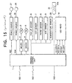
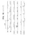
- FIG. 15 is a block diagram of the control circuitry of a conventional electrophotographic printer.
- FIG. 16 is a timing diagram illustrating the operation of the conventional electrophotographic printer.
- the printing control unit 1 in FIG. 15 comprises a microprocessor, read-only memory, random-access memory, input-output ports, timers, and other elements disposed in the printing engine of the printer.
- the printing control unit 1 receives a control signal SG1 and a dot data signal SG2 from a higher-order controller, and controls the printing operations performed by the printing engine.
- the dot data signal SG2 is a one-dimensional digital signal representing a two-dimensional bit map of picture elements (pixels), referred to below as dots.
- the printing control unit 1 Upon receiving a print command via control signal SG1, the printing control unit 1 first checks a temperature sensor 23 to determine whether the fuser 22 is within the necessary temperature range. If the fuser 22 is not within the necessary temperature range, the printing control unit 1 activates a heater 22a built into the fuser 22. When the fuser 22 reaches the necessary temperature, the printing control unit 1 activates a driver 2 that drives a stepping motor or pulse motor (PM) 3 used in the developing and transfer process, and activates a charge signal SGC that switches on a high-voltage power source 25 that charges toner particles in a developer unit 27.
- a temperature sensor 23 Upon receiving a print command via control signal SG1, the printing control unit 1 first checks a temperature sensor 23 to determine whether the fuser 22 is within the necessary temperature range. If the fuser 22 is not within the necessary temperature range, the printing control unit 1 activates a heater 22a built into the fuser 22. When the fuser 22 reaches the necessary temperature, the printing control unit 1 activates a driver 2 that
- the presence or absence of paper and the size of the paper are detected by a paper sensor 8 and size sensor 9. If paper is present, the printing control unit 1 activates a driver 4 that drives another pulse motor (PM) 5. This motor is first driven in reverse by a certain amount, until paper is detected by a pick-up sensor 6, then driven forward to feed the paper into the printing engine.
- PM pulse motor
- the printing control unit 1 sends timing signals SG3 (including horizontal and vertical synchronization signals) to the higher-order controller, and begins receiving the dot data signal SG2, which the higher-order controller generates on a page-at-a-time basis.
- the dot data signal SG2 is supplied as a data signal HD-DATA to an LED head 19 comprising a row of LEDs, with one LED per dot.
- the transfer of dot data into the LED head 19 is synchronized with a clock signal (HD-CLK).
- the printing control unit 1 After sufficient dot data (HD-DATA) for one horizontal dot line have been transferred into the LED head 19, the printing control unit 1 sends the LED head 19 a load signal (HD-LOAD), causing the dot data to be latched in the LED head 19. The LED head 19 can then print this line while receiving dot data for the next line.
- HD-DATA dot data for one horizontal dot line
- HD-LOAD load signal
- the LED head 19 prints the line by illuminating a photosensitive drum (not visible) which has been precharged to a negative electrical potential.
- the potential level of illuminated dots rises, creating a latent dot image.
- the toner in the developer unit 27 is also charged to a negative potential, so toner particles are electrostatically attracted to the illuminated dots, creating a toner image.
- FIG. 16 illustrates the timing of this signal and other signals mentioned above.
- the SG3 pulses shown at the top of FIG. 16 are horizontal synchronization pulses.
- FIG. 16 illustrates three successive line-printing cycles, for printing lines N - 1, N, and N + 1 (where N is an arbitrary integer).
- the printing control unit 1 activates a transfer signal SG4 that turns on a high-voltage power source 26, generating a high positive voltage in a transfer unit 28.
- a transfer signal SG4 that turns on a high-voltage power source 26, generating a high positive voltage in a transfer unit 28.
- the toner image is transferred by electrostatic attraction to the paper.
- the paper with the toner image is then transported to the fuser 22, which has been heated by the heater 22a.
- the heat fuses the toner to the paper, which then passes an exit sensor 7 and is ejected from the printer.
- the printing control unit 1 controls these operations so that the high-voltage power source 26 is switched off except while the paper is traveling past the transfer unit 28, as detected by sensors 6 and 9.
- the printing control unit 1 also switches off the high-voltage power source 25 of the developer unit 27, and stops the pulse motor (PM) 3 used in the developing and transfer process.
- FIG. 17 shows the structure of the conventional LED head 19 in more detail.
- the dot data HD-DATA and clock signal HD-CLK are provided to a shift register comprising, for example, four thousand nine hundred ninety-two flip-flop circuits FF 1 , FF 2 , ... , FF 4992 (this number of flip-flop circuits is appropriate for printing on A4-size paper at six hundred dots per inch).
- the load signal HD-LOAD is activated, causing the bits to be stored in latches LT 1 , LT 2 , ..., LT 4992 .
- bits set to the high logic level ('1') turn on LEDs LD 1 , LD 2 , ..., LD 4992 by way of an inverter G 0 , pre-buffer circuits G 1 , G 2 , ... , G 4992 , and p-channel metal-oxide-semiconductor (MOS) transistors Tr 1 , Tr 2 , ... , Tr 4992 .
- the transistors Tr 1 , Tr 2 , ..., Tr 4992 are the driving elements that allow driving current to flow from the power supply (V DD ) to the anodes of the LEDs LD 1 , LD 2 , ... , LD 4992 .
- the LEDs are disposed on a plurality of LED array chips, which are coupled by bonding wires to integrated driver circuits, referred to below as driver ICs.
- driver ICs integrated driver circuits
- Each LED is individually wire-bonded to an output terminal of the corresponding driver IC.
- the driver ICs (DRV1 to DRV26) are also coupled in a cascaded series to receive the dot data and control signals shown in FIG. 17.
- FIG. 19 shows the internal structure of the first pre-buffer circuit (G 1 ) in FIG. 17, comprising an AND gate AD 1 , a p-channel MOS transistor TP 1 , and an n-channel MOS transistor TN 1 .
- the other pre-buffer circuits G 2 to G 4992 are similar.
- Each driver IC also has a control-voltage generating circuit 209.
- the control-voltage generating circuit 209 comprises an operational amplifier 100, a p-channel MOS transistor 101, and a resistor with resistance R ref .
- the output of the operational amplifier 100 is coupled to all of the pre-buffer circuits in the same driver IC, more specifically to the source terminal of the n-channel MOS transistor in each pre-buffer circuit, e.g., TN 1 in pre-buffer circuit G 1 .
- the p-channel MOS transistor 101 has the same gate length as each of the driving elements Tr 1 , Tr 2 , ..., Tr 4992 .
- the inverting input terminal of the operational amplifier 100 receives a reference voltage V REF from a voltage reference circuit (not visible).
- the operational amplifier 100, p-channel MOS transistor 101, and resistance R ref form a feedback circuit that sets the current I ref flowing through p-channel MOS transistor 101 to ground to a value determined by the reference voltage V REF and resistance R ref , independent of the supply voltage V DD .
- FIG. 20 shows examples of these rise times.
- the upper waveform in FIG. 20 is the waveform of the strobe signal (HD-STB-N).
- the lower waveforms (I D1 ) indicate the driving current supplied to a single LED when one, eight, thirty-two, ninety-six, and one hundred ninety-two LEDs in the same LED array chip are driven simultaneously.
- the rise time of the driving-current waveform (I D1 ) increases markedly.
- the increase in rise time significantly shortens the effective driving time of the LED. Consequently, when many LEDs are driven in the same LED array chip, each illuminated dot receives less light.
- Tr 1 When an LED such as LD 1 in FIG. 19 is driven, it needs to be driven by a current flow that is limited and does not vary, even if the power-supply voltage V DD fluctuates.
- the driving element Tr 1 thus needs to have a high output impedance and must operate with a constant-current characteristic. For these reasons, the driving element Tr 1 must have a comparatively large gate length. To provide adequate driving current to the LED, Tr 1 also has a comparatively large gate width. The large gate area of Tr 1 creates a large gate-source capacitance between the gate electrode wiring pattern and the semiconductor substrate of the driver IC.
- a transient current I 1 flows from the power supply V DD to the output terminal of the operational amplifier 100, mainly through the capacitive coupling between the source and gate of the driving element Tr 1 , charging the gate-source capacitance of Tr 1 , thereby turning Tr 1 on.
- the transient charging current I 1 is well within the current-sinking capability of the operational amplifier 100, despite the large gate-source capacitance of the driving element Tr 1 .
- the total flow of transient charging current from the gate-source capacitances of all of the activated driving elements becomes large enough to be limited by the current-sinking capability of the operational amplifier 100. Due to this limit, as more LEDs are driven, less current is available to charge the gate-source capacitance of each driving element, the driving elements turn on more slowly, and the rise time of the driving current waveforms increases.
- the charging currents I 1 are limited, while the discharging currents I 0 , are not.
- the rise times of the current waveforms are therefore lengthened, with no compensating lengthening of the fall times.
- the illuminated dots receive less light, their diameter is decreased, less toner is transferred, and the printed dots are insufficiently dark.
- a further problem is that when the strobe signal HD-STB-N goes high and the driven LEDs are turned off, the rapid fall of the driving current causes voltage noise at the power-supply leads of the driver ICs.
- the voltage noise ⁇ V at a particular lead is given by the following equation, in which L is the lead inductance, ⁇ i is the total change in driving current supplied through the lead, and ⁇ t is the fall time of the current waveform.
- ⁇ V L ⁇ ( ⁇ i / ⁇ t )
- US 4 734 714 discloses an optical printer including an optical printing head and a photosensitive member. Although quiet and fine printing can be performed when a light emitting diode array is employed as the optical printing head, there have been problems, on the other hand, such as difficulty in driving and difficulty in adjustment of primary factors directly affecting the printing quality such as uneveness in dot pitches and intensity. Therefore, US 4 734 714 copes with driving conditions by effectively distributing data transferring during static driving, thereby to improve the printing quality by selective printing timings.
- WO 92/00196 discloses a non-impact printer apparatus including a recording head having a plurality of recording elements (30) such as LED's for recording on a recording medium (12).
- a plurality of driver chips (40) are provided on the head and each includes a plurality of current driving channels for selectively driving a plurality of recording elements in accordance with respective image data signals.
- the driver chips (40) each further include an extra current driving channel not associated with a recording element (30) for generating a current related to that sent to said recording elements. Monitoring of the current in the extra channel is provided to permit for changes of current to the recording elements (30) and/or corrected image data to provide fine tuned control over uniformity of the recording elements.
- a digitally adjustable current mirror controls the level of current to each LED during recording.
- Digital current data signals for controlling this level of current are also communicated over one of the lines of the data bus.
- Token bit signals are used to control the latching of both current data signals and image data signals in respective registers storing the digital data used for current control and the image data used for controlling energization times.
- Each driver chip (40) includes two sets of digitally addressable transistors. This allows for individual chip control of current to the respective LED's to correct for nonuniformity of light output from chip to chip due to temperature gradients as well as controlling for light output due to aging of the printhead.
- the current mirror has a master circuit for generating a reference current and a plurality of slave circuits for providing respective driver currents to the recording elements (30) selected for energization.
- a transistor switch is in series with a respective recording element (30) and switchable from one state to another in response to a signal at its control electrode.
- Each of the slave circuits includes an additional slave circuit which provides a current path for facilitating changing of the signal at the control electrode from one voltage level to another such as by allowing a capacitive charge at the control electrode to dissipate.
- US 4967192 discloses a driver IC of a light-emitting diode array head for an electronic photograph printer including a current mirror circuit having a reference element and at least an output element so as to produce a reference current by use of a digital signal as an input thereto, a reference current source capable of outputting a plurality of reference current values, a selection circuit for specifying and selecting one of a plurality of reference current values from the reference current source to be applied as an input current to the current mirror circuit, and an output control circuit for controlling the on and off states of an output current to be supplied to the output element of the current mirror circuit in accordance with a light emission control signal externally supplied.
- the output control circuit achieves a multi-stage control of the driver output current volume, which is to be delivered to the light emitting diodes, thereby facilitating the driving operation to correct the fluctuation in the light emission power of the light-emitting diode array and the change of the light emission power thereof with the lapse of time.
- Another object of the invention is to reduce voltage noise when the current supplied to the driven elements is switched off.
- Another object is to provide an LED head in which the above objects are achieved.
- each driven element is driven by a first driving element and a second driving element coupled in series.
- the first driving element sets the driving current to a predetermined value.
- the second driving element switches the driving current on and off.
- the first driving element operates statically.
- a substantially unlimited number of first driving elements can be coupled to the same control-voltage generating circuit without stressing the output capabilities of the control-voltage generating circuit.
- a plurality of driven elements are driven by respective driving elements, which are switched on and off by respective pre-stage circuits.
- the pre-stage circuits are all coupled to a single control-voltage generating circuit, which supplies a control voltage used for switching the driving elements on.
- a resistor is inserted in series between each driving element and its pre-stage circuit.
- the resistors limit transient current flow to a value within the output capability of the control-voltage generating circuit, even when all of the driving elements are switched on simultaneously.
- the resistors also reduce voltage noise by making the driving elements turn off relatively slowly.
- a plurality of driven elements are driven by respective driving elements, which are switched on and off by respective pre-stage circuits, all coupled to a single control-voltage generating circuit as in the second aspect of the invention.
- the pre-stage circuits operate with constant-current output characteristics.
- the control-voltage generating circuit can be designed to provide the necessary output current, even when all driven elements are driven simultaneously.
- the constant-current characteristics can also be set so that the driven elements turn off slowly, thereby reducing voltage noise.
- the embodiments are driving circuits used in the LED head 19 of an electrophotographic printer of the type shown in FIG. 15.
- FIG. 1 is a block diagram showing the general structure of the LED head 19 in all of the embodiments described below.
- the LED head comprises twenty-six LED array chips 201, twenty-six driver ICs 202, and a reference-voltage generating circuit 203.
- Each LED array chip 201 has a linear array of one hundred ninety-two LEDs (not visible).
- Each driver IC 202 has circuits for driving these LEDs, including a shift register 204, a latch circuit 205, an inverter 206, a gate circuit 207, an LED driving circuit 208, and a control-voltage generating circuit 209.
- the shift register 204 comprises one hundred ninety-two flip-flop circuits through which printing data (HD-DATA) are shifted in synchronization with a clock signal (HD-CLK).
- the latch circuit 205 latches all bits of data stored in the shift register 204 at once, in synchronization with a load signal (HD-LOAD).
- the inverter 206 converts the strobe signal (HD-STB-N) from negative logic to positive logic for input to the gate circuit 207.
- the gate circuit 207 comprises one hundred ninety-two AND gates, each receiving the inverted strobe signal output by the inverter 206 and one bit of latched printing data output from the latch circuit 205.
- the LED driving circuit 208 comprises one hundred ninety-two parallel driving circuits that supply driving current to the LEDs in the LED array chip 201, in response to the outputs of the gate circuit 207.
- the control-voltage generating circuit 209 generates a control voltage that controls the current value of the driving current.
- the printing data (HD-DATA), clock signal (HD-CLK), load signal (HD-LOAD), and strobe signal (HD-STB-N) are supplied from the printing control unit 1 in FIG. 15.
- the LED head preferably also has temperature compensation circuits and circuits for compensating for dot-to-dot and chip-to-chip differences. For simplicity, these compensation circuits are omitted from the drawings.
- FIG . 2 shows the circuit structure of one of the one hundred ninety-two parallel driving circuits in the LED driving circuit 208 in a first embodiment of the invention.
- the driving circuit comprises a p-channel MOS transistor TP 1 , an n-channel MOS transistor TN 1 , and a further pair of p-channel MOS transistors M 1 and M 2 .
- Transistors M 1 and M 2 are the driving elements.
- Transistor M 1 functions as a current-limiting element; transistor M 2 , as a switching element.
- the source terminal of p-channel MOS transistor TP 1 is coupled to a power-supply node, and receives the power-supply potential V DD .
- the source terminal of n-channel MOS transistor TN 1 is coupled to ground.
- the drain terminals of transistors TP 1 and TN 1 are mutually interconnected.
- the gate terminals of transistors TP 1 and TN 1 are both coupled to the output of an AND gate in the gate circuit 207, so that transistors TP 1 and TN 1 function as an inverter.
- These transistors TP 1 and TN 1 and the AND gate form a pre-stage circuit or pre-buffer circuit G 1 , which has the inverter comprising transistors TP 1 and TN 1 as its output stage.
- the source terminal of p-channel MOS transistor M 1 is coupled to the power-supply (V DD ) node.
- the drain terminal of p-channel MOS transistor M 1 is coupled to the source terminal of p-channel MOS transistor M 2 .
- the drain terminal of p-channel MOS transistor M 2 is coupled to an output terminal 310 of the driver IC 202.
- the output terminal 310 is coupled to the anode of an LED (LD 1 ) in one of the LED array chips 201 shown in FIG. 1.
- the cathode of LD 1 is coupled to ground.
- the gate terminal of transistor M 2 is coupled to the drain terminal of transistor TP 1 ; that is, to the output of the inverter comprising transistors TP 1 and TN 1 .
- the gate terminal of transistor M 1 is coupled to the output terminal of the control-voltage generating circuit 209.
- the control-voltage generating circuit 209 has the conventional structure, comprising an operational amplifier 100, a p-channel MOS transistor 101, and a resistor with resistance R ref ⁇
- the reference voltage V REF is supplied from the reference-voltage generating circuit 203 in FIG. 1.
- the gate terminal of p-channel MOS transistor M 1 and the gate terminal of p-channel MOS transistor 101 are both coupled to the output terminal of the operational amplifier 100, and receive the control voltage V control .
- All of the transistors shown in FIG. 2 are fabricated by a semiconductor fabrication process with a design rule that sets a minimum size for gate lengths, gate widths, and other features.
- the gate lengths of p-channel MOS transistors 101 and M 1 are identically larger than this minimum feature size.
- the gate width of p-channel MOS transistor M 1 is also larger than the minimum feature size.
- the gate width of p-channel MOS transistor M 2 is, for example, the same as the gate width of p-channel MOS transistor M 1 .
- the gate length of p-channel MOS transistor M 2 is equal to the minimum feature size.
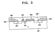
- FIG. 3 is a sectional view of the structure of p-channel MOS transistors M 1 and M 2 , which are formed in an n-type semiconductor substrate 301.
- the source and drain regions of these transistors comprise p-type diffusions 302.
- Interconnecting lines 303 and 304 made in a metal wiring layer, lead to the power-supply node marked V DD in FIG. 2 and to the output terminal 310, respectively.
- the interconnecting lines 303, 304 are isolated from the semiconductor substrate 301 by an oxide insulating layer 305.
- the gate electrodes 306 and 307 are similarly insulated by an oxide layer from the semiconductor substrate 301.
- the long gate electrode 306 is the gate terminal of p-channel MOS transistor M 1 ; the short gate electrode 307 is the gate terminal of p-channel MOS transistor M 2 .
- the combined size of transistors M 1 and M 2 is reduced by placing their gate electrodes 306, 307 side by side.
- the gate electrodes 306, 307 and interconnecting lines 303, 304 are covered with a glass insulating layer 308.
- the gate potential of the p-channel MOS transistor 101 is controlled by feedback through the operational amplifier 100 to maintain a constant reference current I ref equal to the reference voltage V REF divided by the resistance R ref .
- the values of V REF and R ref are selected so that transistor 101 operates in its saturation region, in which I ref is determined by the gate-source voltage of transistor 101, which is equal to the difference between the supply voltage V DD and the control voltage V control .
- the operational amplifier 100 varies V control to follow any variations in V DD , keeping the gate-source voltage of transistor 101 constant.
- the gate-source voltage of transistor M 1 is also equal to the difference between V DD and V control . Since the operational amplifier 100 holds this difference constant, there is no flow of charging or discharging current into the gate-source capacitance of transistor M 1 . Transistor M 1 is always turned on. When the switching transistor M 2 is also turned on, transistor M 1 immediately allows a predetermined driving current I D1 to flow to the driven LED (LD 1 ).
- transistor M 1 Since transistor M 1 has the same gate-source voltage and the same gate length as the p-channel MOS transistor 101 in the control-voltage generating circuit 209, these two transistors form a current mirror, and the driving current I D1 is proportional to the reference current I ref . Transistor M 1 operates in its saturation region, and the driving current I D1 is held substantially constant, regardless of variations in the power-supply or ground potential.
- the gate-source capacitance of transistor M 2 is comparatively small, because of the minimal length of the gate electrode 307.
- the gate electrode 307 of transistor M 2 is quickly charged to the ground potential by a transient current flow through n-channel MOS transistor TN 1 , and transistor M 2 turns on.
- the gate electrode 307 quickly discharges to the V DD potential through p-channel MOS transistor TP 1 , and transistor M 2 turns off.
- the turn-on and turn-off times are substantially unaffected by the number of dots driven simultaneously, because the charging and discharging currents flow through a different transistor for each dot.
- a '1' is loaded from the shift register 204 in FIG. 1 into the latch LT 1 in FIG. 2.
- the loading occurs while the strobe signal HD-STB-N is high, making the output of inverter 206 and the outputs of all AND gates in the gate circuit 207 low.
- the low output of the AND gate in FIG. 2 is inverted by the inverter comprising transistors TP 1 and TN 1 .
- the pre-buffer circuit G 1 is therefore in the high output state, and the switching transistor M 2 is turned off.
- FIG. 4 shows waveforms illustrating these operations.
- the upper waveform is the waveform of the strobe signal HD-STB-N; the lower waveforms indicate the driving current I D1 supplied to LED LD 1 when one, eight, thirty-two, ninety-six, and one hundred ninety-two LEDs are driven simultaneously by the same driver IC 202.
- LEDs driven dots
- each LED is driven by two p-channel MOS transistors M 1 and M 2 coupled in series.
- Transistor M 1 which has a long gate length and comparatively low saturation current, limits the driving current to a desired constant value.
- Transistor M 2 which has a minimal gate length, switches the driving current on and off.
- the current-limiting transistor M 1 operates in a completely static manner, without being affected by the number of dots driven simultaneously.
- the switching transistor M 2 is driven by an independent pre-buffer circuit for each dot, so its operation is also substantially unaffected by the number of dots driven simultaneously; in particular, its transient characteristics (rise time and fall time) are substantially unaffected.
- the LED driving circuit 208 in the second embodiment also has a pre-buffer circuit G 1 with an output stage, comprising a p-channel MOS transistor TP 1 and an n-channel MOS transistor TN 1 , that inverts the output of an AND gate in the gate circuit 207.
- the source of transistor TP 1 is coupled to the power supply V DD , but the source of transistor TN 1 is coupled to the output terminal of the operational amplifier 100 in the control-voltage generating circuit 209, as in the prior art.
- the control voltage V control functions as the ground potential of the output stage of the pre-buffer circuit G 1 .
- the drain terminals of transistors TP 1 and TN 1 are coupled through a current-limiting resistor R P to the gate of a p-channel MOS transistor Tr 1 .
- the resistance of resistor R P is preferably at least one hundred ohms (100 ⁇ ), but not more than ten thousand ohms (10 k ⁇ ).
- the p-channel MOS transistor Tr 1 is the driving element. Its source terminal is coupled to the power supply V DD ; its drain terminal is coupled to an output terminal 310 of the driver IC 202, thus to the anode of a driven LED (LD 1 ).
- Transistor Tr 1 has a comparatively long and wide gate electrode, the gate length matching the gate length of the p-channel MOS transistor 101 in the control-voltage generating circuit 209.
- transistor Tr 1 When p-channel MOS transistor TP 1 is turned off and n-channel MOS transistor TN 1 is turned on, p-channel MOS transistor Tr 1 and p-channel MOS transistor 101 have the same source potential (V DD ) and gate potential (V control ), and form a current mirror. In this state, transistor Tr 1 supplies LED LD 1 with a predetermined driving current I D1 , proportional to the reference current I ref .
- p-channel MOS transistor TP 1 When p-channel MOS transistor TP 1 is turned on and n-channel MOS transistor TN 1 is turned off, p-channel MOS transistor Tr 1 is turned off and driving current I D1 ceases to flow.
- a '1' is loaded from the shift register 204 into the latch LT 1 , then the strobe signal HD-STB-N is asserted.
- the low logic level of the strobe signal is inverted by the inverter 206, passed through the gate circuit 207, then inverted again by the inverter comprising transistors TP 1 and TN 1 , the output potential of which changes from V DD to the control voltage V control .
- the gate potential of p-channel MOS transistor Tr 1 is thereby reduced to V control , causing transistor Tr 1 to turn on.
- a transient current I 1 flows from the power supply V DD to the output terminal of the operational amplifier 100, mainly through the capacitive coupling between the gate electrode of p-channel MOS transistor Tr 1 and the semiconductor substrate of the driver IC, charging the gate-source capacitance.
- This transient current I 1 is forced to flow through the current-limiting resistor R P , the resistance of which is high enough to assure that even if a large number of dots are driven simultaneously, the total transient current flow will be within the current-sinking capability of the operational amplifier 100.
- the transition times (rise time and fall time) of the LED driving current are, accordingly, substantially unaffected by the number of dots driven simultaneously, and are long enough to suppress potentially harmful voltage noise.
- FIG. 6 shows waveforms of the strobe signal HD-STB-N and the LED driving current I D1 in the second embodiment.
- the driving current waveforms shown in the lower part of the drawing are labeled according to the number of dots driven simultaneously, from one to one hundred ninety-two. Both the rise times and the fall times are lengthened, as compared with the first embodiment. Although there is some difference in the rise times of the driving current waveforms, depending on the number of driven dots, the difference is not nearly as large as in the prior art (FIG. 20). There is very little difference in the fall times ⁇ t.
- a current-limiting resistor is inserted between the pre-buffer circuit G 1 and the driving element Tr 1 , so that even when all dots are driven simultaneously, the total transient current is within the current-sinking capability of the operational amplifier 100.
- the dependence of the turn-on time of the driving element Tr 1 on the number of driven dots is thereby reduced to a level that can be ignored in practice.
- the turn-off times of the driving elements are also lengthened, reducing voltage noise at IC leads.
- the LED driving circuit 208 in the third embodiment has a circuit topology similar to that of the second embodiment without the current-limiting resistor R P .
- the drain terminals of p-channel MOS transistor TP 1 and an n-channel MOS transistor TN 1 in the output stage of the pre-buffer circuit G 1 are coupled directly to the gate terminal of p-channel MOS transistor Tr 1 , which is the driving element.
- a feature of the third embodiment is that the n-channel MOS transistor TN 1 has a comparatively long gate length, causing the pre-buffer circuit G 1 to operate with a substantially constant-current output characteristic when charging the gate-source capacitance of the driving element Tr 1 .
- the gate potential of transistor TN 1 is the power-supply potential V DD , while its source potential is the V control potential output by the control-voltage generating circuit 209.
- the gate-source voltage (V GS ) of transistor TN 1 is accordingly the difference between V DD and V control .
- V DD is five volts (5 V)
- V control is 3.4 V
- V GS is 1.6 V.
- FIG. 8 shows examples of the drain current characteristic of the n-channel MOS transistor TN 1 for gate lengths L of one micrometer (1 ⁇ m, curve a) and five micrometers (5 ⁇ m, curve b).
- Drain current (I D ) is indicated in microamperes ( ⁇ A) on the vertical axis, and drain-source voltage (V DS ) in volts on the horizontal axis. Both characteristics assume a gate-source voltage V GS of 1.6 V.
- the region to the left of the dotted line, in which the drain-source voltage V DS is equal to or less than the gate-source voltage V GS is of particular interest in the present embodiment.
- FIG. 8 shows examples of the drain current characteristic of the n-channel MOS transistor TN 1 for gate lengths L of one micrometer (1 ⁇ m, curve a) and five micrometers (5 ⁇ m, curve b).
- Drain current (I D ) is indicated in microamperes ( ⁇ A) on the vertical axis, and drain-
- the drain current I D can be limited to a small value (less than 20 ⁇ A for a 5- ⁇ m gate length), and transistor TN 1 can be made to operate at this limited value with a substantially constant-current characteristic over most of the region of interest (V DS ⁇ 1.6 V).
- Increasing the gate length L reduces the saturation current I DSS by reducing W/L, and by increasing the threshold voltage V t .
- the increase in V t also enlarges the saturation region.
- FIG. 9 shows the internal structure of the operational amplifier 100 in the third embodiment, comprising a resistor 320, p-channel MOS transistors 321, 322, 323, n-channel MOS transistors 324, 325, 326, 327, 328, and a capacitor 329.
- Resistor 320 is coupled in series with n-channel MOS transistor 324 to generate a bias voltage V B , which is applied to the gate electrodes of n-channel MOS transistors 324, 325, 326, permitting substantially constant currents I B , I 2 , and I 3 to flow.
- the p-channel MOS transistors 321, 322 and n-channel MOS transistors 325, 327, 328 form a differential amplifying circuit.
- the gate terminal of transistor 328 is the noninverting input terminal (+) of the operational amplifier 100;
- the gate n-channel MOS transistor 327 is the inverting input terminal (-).
- the p-channel MOS transistor 323 and n-channel MOS transistor 326 form an output amplifying circuit, the drain terminals of both of these transistors being coupled to the output terminal of the operational amplifier 100.
- the current-sinking capability of the operational amplifier 100 is limited by the saturation current I 3 of n-channel MOS transistor 326.
- this saturation current I 3 is at least one hundred ninety-two times the saturation current I DSS of the n-channel MOS transistor TN 1 in the pre-buffer circuit G 1 . Since I DSS is limited to a small value, the necessary value of I 3 can be obtained with practical values of the bias voltage V B and the gate width and length of n-channel MOS transistor 326.
- the other circuit elements in the third embodiment are the same as in the prior art.
- the p-channel MOS transistor TP 1 has a minimal gate length.
- the gate-source capacitance of p-channel MOS transistor Tr 1 is charged by a transient current flow I 1 through n-channel MOS transistor TN 1 , reducing the gate potential of transistor Tr 1 from V DD to V control .
- n-channel MOS transistor TN 1 turns on, its drain-source voltage is equal to the difference between V DD and V control , and is therefore the same as its gate source voltage V GS (1.6 V).
- FIG. 10 indicates the subsequent operation of n-channel MOS transistor TN 1 , showing the charging current I 1 on the vertical axis and the drain-source voltage V DS on the horizontal axis.
- charging current I 1 flows at the saturation level I DSS of transistor TN 1 .
- the drain-source voltage of transistor TN 1 falls together with the gate potential of transistor Tr 1 , but charging current I 1 continues to flow at substantially the same rate until about point B.
- the saturation region is usually defined to be the region to the right of the dashed line, in which the drain-source voltage V DS exceeds the difference between the gate-source voltage V GS and threshold voltage V t , but because of the long gate length of transistor TN 1 , the current flow remains nearly saturated for some distance to the left of this line.
- the gate-source capacitance of transistor Tr 1 has been almost completely charged. The charging process is completed at lower current levels from point B to point C.
- the charging current I 1 depicted in FIG. 10 becomes part of the current I 3 in FIG. 9. Since the saturation current of transistor 326 is at least one hundred ninety-two times the saturation current of transistor TN 1 , all of the charging current flow shown in FIG. 10 can be absorbed into the current I 3 in FIG. 9, even if all one hundred ninety-two dots are driven simultaneously.
- FIG. 11 shows the strobe signal waveform (HD-STB-N) and driving current waveforms (I D1 ) for LED LD 1 when one, eight, thirty-two, ninety-six, and one hundred ninety-two dots are driven simultaneously. Since the charging current is limited by n-channel MOS transistor TN 1 rather than by the current-sinking capability of the operational amplifier 100, all of the current-driving waveforms I D1 are substantially identical. The rise time of the driving current is substantially independent of the number of driven dots.
- n-channel MOS transistor TN 1 is conventionally given a minimum gate length, to minimize the turn-on time of the driving element Tr 1 .
- n-channel MOS transistor TN 1 has a drain current characteristic similar to curve a, for example, in FIG. 8, rising to a comparatively high level in the region of interest (V DS ⁇ V GS ), instead of being held to a constant low level. Under these conditions, it becomes impractical to design the operational amplifier 100 to sink charging current from the pre-buffer circuits of all dots at once.
- the LED driving circuit 208 in the fourth embodiment comprises p-channel MOS transistors TP 0 , TP 1 , Tr 1 , and n-channel MOS transistors TN 0 and TN 1 .
- the driving element Tr 1 and n-channel MOS transistor TN 1 are identical to the corresponding elements in the third embodiment, both having longer-than-minimum gate lengths.
- the gate length of p-channel MOS transistor TP 1 is also longer than the minimum length, although still shorter than the gate length of n-channel MOS transistor TN 1 .
- transistors TP 0 and TN 0 form an intermediate stage between a NAND gate ND 1 and the output stage, which comprises transistors TP 1 and TN 1 .
- Transistors TP 0 and TN 0 constitute an inverter that, combined with NAND gate ND 1 , forms an AND gate in the gate circuit 207.
- the low AND logic level output in the fourth embodiment is the control voltage V control , which is supplied instead of the ground potential to the source terminal of n-channel MOS transistor TN 0 .
- the control voltage V control thus functions as the ground potential of both the intermediate stage and the output stage of the pre-buffer circuit G 1 .
- the other elements in the fourth embodiment are identical to the corresponding elements in the third embodiment.
- the strobe signal (HD-STB-N) When the strobe signal (HD-STB-N) is driven low, it is inverted three times, by inverter 206, NAND gate ND 1 , and the inverter comprising transistors TP 0 and TN 0 , resulting in high output, at the V DD potential, from p-channel MOS transistor TP 0 to the gate electrodes of transistors TP 1 and TN 1 .
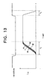
- the n-channel MOS transistor TN 1 operates just as in the third embodiment, conducting a substantially constant current I 1 that charges the gate-source capacitance of the driving element Tr 1 at a controlled rate. Referring to FIG. 13, the driving current waveform (I D1 ) rises in the same amount of time T r , regardless of the number of driven dots.
- n-channel MOS transistor TN 0 supplies the control voltage V control to the gate electrodes of transistors TP 1 and TN 1 .
- the n-channel MOS transistor TN 1 turns off because its gate-source voltage is now zero.
- the gate-source voltage V GS of the p-channel MOS transistor TP 1 is equal to the difference between V control and the power-supply potential V DD . This difference is held to a constant value (1.6 V) by the control-voltage generating circuit 209, and is large enough to turn on transistor TP 1 , causing discharging current I 0 to flow into the gate terminal of the driving element Tr 1 .
- transistor TP 1 Due to the increased gate length of p-channel MOS transistor TP 1 , and to its comparatively small and precisely controlled gate-source voltage V GS (1.6 V), transistor TP 1 operates with a constant-current characteristic.
- the discharging current I 0 in the fourth embodiment is limited to a comparatively small value, and the driving element Tr 1 turns off more slowly than in the third embodiment, increasing the fall time T f of the driving current (I D1 ), as shown in FIG. 13. Since p-channel MOS transistor TP 1 has a shorter gate length than n-channel MOS transistor TN 1 , the fall time T f is shorter than the rise time T r .
- the increased fall time T f reduces the amount of voltage noise generated at the power-supply leads of the driver IC 202, the voltage noise being inversely proportional to T f .
- the constant-current characteristic with which p-channel MOS transistor TP 1 operates enables the fall time T f to be set to a desired value by suitable design of the dimensions of transistor TP 1 , so that voltage noise can be reduced to a desired level through simple design calculations.
- the pre-buffer circuit by providing the pre-buffer circuit with constant-current output characteristics for both charging and discharging current, a uniform rise time of the LED driving current is obtained, regardless of the number of driven dots, and the voltage noise caused by the discharging current is reduced to a controllable, harmless level.
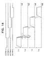
- FIG. 14 illustrates a variation of the fourth embodiment, in which the LED head is divided lengthwise into four blocks, with respective strobe signals HD-STB1-N, HD-STB2-N, HD-STB3-N, HD-STB4-N.
- Each driver IC 202 receives one of these four strobe signals.
- the strobe timing is staggered so that at most one-fourth of the LEDs in the LED head are driven simultaneously, thereby limiting the total driving current flowing at any one time to a maximum value that can be provided by a small and inexpensive power supply.
- the current-limiting transistors of the second embodiment can be used to increase the turn-on and turn-off times of the switching transistors M 2 in the first embodiment, to reduce voltage noise.
Landscapes
- Physics & Mathematics (AREA)
- Engineering & Computer Science (AREA)
- Optics & Photonics (AREA)
- General Engineering & Computer Science (AREA)
- General Physics & Mathematics (AREA)
- Theoretical Computer Science (AREA)
- Printers Or Recording Devices Using Electromagnetic And Radiation Means (AREA)
- Semiconductor Lasers (AREA)
- Led Devices (AREA)
- Control Of Indicators Other Than Cathode Ray Tubes (AREA)
Claims (14)
- Treiberschaltung, die einen Treiberstrom an eine Vielzahl angetriebener Elemente (LD1) zuführt, umfassend:eine Steuerspannung-Generatorschaltung (209), die eine Steuerspannung erzeugt; undeine Vielzahl von Treibereinheiten (208), wobei jede separat umfasst:ein erstes Treiberelement (M1) das einen Steueranschluß hat, der die Steuerspannung von der Steuerspannung-Generatorschaltung (209) empfängt, wobei das erste Treiberelement (M1) einen konstanten Treiberstrom an eines der angetriebenen Elemente (LD1) liefert, wobei die Steuerspannung einen Stromwert des Treiberstrom bestimmt;ein zweites Treiberelement (M2), das einen Steueranschluß hat, der in Reihe mit dem ersten Treiberelement (M1) geschaltet ist und den Treiberstrom ein- und ausschaltet;einen Inverter (TP1, TN1), der mit seinem Ausgang an dem Steueranschluß des zweiten Treiberelements (M2) gekoppelt ist und der den Steueranschluß des zweiten Treiberelements (M2) lädt und entlädt, um das zweite Treiberelement (M2) ein und auszuschalten.
- Treiberschaltung nach Anspruch 1, worin das angetriebene Elemente (LD1) ein Licht emittierendes Element mit einer Anode ist, die ersten und zweiten Treiberelemente (M1 und M2) MOS Transistoren mit einer Source-Elektrode, einer Gate-Elektrode und einer Drain-Elektrode sind, wobei die Gate-Elektrode des zweiten Treiberelements (M2) der Steueranschluß ist, die Gate-Elektrode des ersten Treiberelements (M1) mit der Steuerspannung - Generatorschaltung (209) gekoppelt ist, die Source-Elektrode des ersten Treiberelements mit einer Stromquelle gekoppelt ist, die Drain-Elektrode des ersten Treiberelements mit der Source-Elektrode des zweiten Treiberelements (M2) gekoppelt ist und die Drain-Elektrode des zweiten Treiberelements mit der Anode des angetriebenen Elements gekoppelt ist.
- Treiberschaltung nach Anspruch 1, wobei die ersten und zweiten Treiberelemente (M1 und M2) MOS Transistoren sind, die jeweils eine Source-Elektrode eine Gate-Elektrode und eine Drain-Elektrode haben, wobei die Gate-Elektrode des zweiten Treiberelements (M2) mit dem Steueranschluß gekoppelt ist, wobei das erste Treiberelement (M1) und das zweite Treiberelement (M2) durch ein Halbleiterherstellungsverfahren hergestellt sind, das eine vorgegebene, minimale Gate-Länge gestattet, wobei das Gate des ersten Treiberelements länger ist als die minimale Gate-Länge und die Gate-Elektrode des zweiten Treiberelements die minimale Gate-Länge hat.
- Treiberschaltung mit einer Vielzahl von Treiberelementen (Tr1), die einen Treiberstrom von einer Stromquelle an jeweilige angetriebene Elemente (LD1) zuführen, umfassend:eine Steuerspannung-Generatorschaltung (209), die eine Steuerspannung erzeugt;eine Vielzahl von Vorstufenschaltungen (G1), die mit der Steuerspannung-Generatorschaltung (209) gekoppelt sind und die Steuerspannung benutzen, um entsprechende Treiberelemente (Tr1) einzuschalten; undeine Vielzahl von Strombegrenzer-Widerständen (RP) die in Reihe zwischen den Vorstufenschaltungen (G1) und den entsprechenden Treiberelementen (Tr1) angekoppelt sind und den Stromfluß zwischen den Treiberelementen und der Steuerspannung-Generatorschaltung (209) begrenzen.
- Treiberschaltung nach Anspruch 4, worin die Treiberelemente (Tr1) MOS Transistoren mit jeweiligen Gate-Elektroden sind, und wobei die Strombegrenzer -Widerstände zwischen den Gate-Elektroden und den jeweiligen Vorstufenschaltungen angekoppelt sind.
- Treiberschaltung mit einer Vielzahl von Treiberelementen (Tr1), die einen Treiberstrom von einer Stromquelle an entsprechende angetriebene Elemente (LD1) zuführen, umfassend:eine Steuerspannung-Generatorschaltung (209), die eine Steuerspannung erzeugt;eine Vielzahl von Vorstufenschaltungen (G1), die mit der Steuerspannung-Generatorschaltung (209) gekoppelt sind und die Steuerspannung benutzen, um die jeweiligen Treiberelemente (Tr1) einzuschalten, wobei die Vorstufenschaltungen mit Konstantspannungs-Ausgangscharakteristiken arbeiten, die den Stromfluss zwischen den Treiberelementen und der Steuerspannung-Generatorschaltung begrenzen.
- Treiberschaltung nach Anspruch 6, worin jede der Vorstufenschaltungen (G1) eine Ausgangsstufe hat, und worin die Steuerspannung als Erdpotential der Ausgangsstufe verwendet wird.
- Treiberschaltung nach Anspruch 7, worin jeder der Vorstufenschaltungen (G1) auch eine Zwischenstufe hat, die die Ausgangsstufe treibt, und wobei die Steuerspannung auch als Erdpotential der Zwischenstufe verwendet wird.
- Treiberschaltung nach Anspruch 6, worin die Vorstufenschaltungen (G1) MOS Transistoren (TN1) aufweisen, die durch ein Halbleiterherstellungsverfahren hergestellt sind, das einen vorgegebene, minimale Gate-Länge gestattet, und wobei die Konstantstromcharakteristiken dadurch erhalten werden, dass wenigstens einige der MOS Transistoren mit Gate-Elektroden ausgestattet werden, die länger als die minimale Gate-Länge sind.
- Treiberschaltung nach Anspruch 9, worin jede der Vorstufenschaltungen (G1) eine Ausgangsstufe hat, die ein komplementäres Paar von MOS Transistoren (TP1, TN1) umfasst, die in Reihe zwischen der Steuerspannung-Generatorschaltung (209) und der Stromquelle angekoppelt sind.
- Treiberschaltung nach Anspruch 10, wobei einer der MOS Transistoren (TN1) in dem komplementären Paar eine Gate-Elektrode hat, die länger als die minimale Gate-Länge ist.
- Treiberschaltung nach Anspruch 10, worin beide der MOS Transistoren (TP1, TN1) in dem komplementären Paar Gate-Elektroden haben, die länger als die minimale Gate-Länge sind.
- Treiberschaltung nach Anspruch 12, worin jede der Vorstufenschaltungen (G1) auch eine Zwischenstufe hat, die schaltbar die Steuerspannung an die Gate-Elektroden von beiden MOS Transistoren (TP1, TN1) in dem komplementären Paar liefert.
- LED-Kopf umfassend eine Treiberschaltung nach einem der Ansprüche 1 oder 4, worin die angetriebenen Elemente (LD1) Licht emittierende Dioden sind.
Applications Claiming Priority (4)
| Application Number | Priority Date | Filing Date | Title |
|---|---|---|---|
| JP2873598 | 1998-02-10 | ||
| JP2873598 | 1998-02-10 | ||
| JP26992698 | 1998-09-24 | ||
| JP26992698A JP3732345B2 (ja) | 1998-02-10 | 1998-09-24 | 駆動回路、ledヘッド及びプリンタ |
Publications (3)
| Publication Number | Publication Date |
|---|---|
| EP0936509A2 EP0936509A2 (de) | 1999-08-18 |
| EP0936509A3 EP0936509A3 (de) | 2000-01-05 |
| EP0936509B1 true EP0936509B1 (de) | 2006-07-19 |
Family
ID=26366884
Family Applications (1)
| Application Number | Title | Priority Date | Filing Date |
|---|---|---|---|
| EP99102167A Expired - Lifetime EP0936509B1 (de) | 1998-02-10 | 1999-02-03 | Treiberschaltung und LED-Kopf mit konstanter Einschaltzeit |
Country Status (4)
| Country | Link |
|---|---|
| US (1) | US6400349B1 (de) |
| EP (1) | EP0936509B1 (de) |
| JP (1) | JP3732345B2 (de) |
| DE (1) | DE69932373T2 (de) |
Families Citing this family (30)
| Publication number | Priority date | Publication date | Assignee | Title |
|---|---|---|---|---|
| US6501449B1 (en) * | 1999-12-08 | 2002-12-31 | Industrial Technology Research Institute | High matching precision OLED driver by using a current-cascaded method |
| JP2001326569A (ja) * | 2000-05-16 | 2001-11-22 | Toshiba Corp | Led駆動回路及び光送信モジュール |
| JP3769180B2 (ja) * | 2000-09-26 | 2006-04-19 | 株式会社東芝 | 発光ダイオード駆動回路およびそれを用いた光送信モジュール |
| JP3957150B2 (ja) * | 2001-02-08 | 2007-08-15 | セイコーインスツル株式会社 | Led駆動回路 |
| JP3859483B2 (ja) | 2001-10-26 | 2006-12-20 | 沖電気工業株式会社 | 駆動回路 |
| JP3723507B2 (ja) * | 2002-01-29 | 2005-12-07 | 三洋電機株式会社 | 駆動回路 |
| JP2003308030A (ja) * | 2002-02-18 | 2003-10-31 | Sanyo Electric Co Ltd | 表示装置 |
| JP2004017634A (ja) * | 2002-06-20 | 2004-01-22 | Konica Minolta Holdings Inc | 画像露光装置 |
| US20050212857A1 (en) * | 2002-11-29 | 2005-09-29 | Canon Kabushiki Kaisha | Recording head and recorder comprising such recording head |
| JP3927902B2 (ja) * | 2002-11-29 | 2007-06-13 | キヤノン株式会社 | インクジェット記録ヘッド及び当該記録ヘッドを有するインクジェット記録装置及びインクジェット記録ヘッド用基板 |
| US7944411B2 (en) * | 2003-02-06 | 2011-05-17 | Nec Electronics | Current-drive circuit and apparatus for display panel |
| TWI230914B (en) * | 2003-03-12 | 2005-04-11 | Au Optronics Corp | Circuit of current driving active matrix organic light emitting diode pixel and driving method thereof |
| JP4581347B2 (ja) * | 2003-08-08 | 2010-11-17 | 富士ゼロックス株式会社 | 発光素子駆動装置及び画像形成装置 |
| TWI244982B (en) * | 2003-11-11 | 2005-12-11 | Canon Kk | Printhead, printhead substrate, ink cartridge, and printing apparatus having printhead |
| JP2005153343A (ja) | 2003-11-26 | 2005-06-16 | Oki Data Corp | 素子駆動方法、素子駆動装置及びプリンタ |
| CN100336090C (zh) * | 2003-12-15 | 2007-09-05 | 友达光电股份有限公司 | 电流驱动式平面显示器的驱动电路 |
| JP4274097B2 (ja) * | 2004-09-29 | 2009-06-03 | セイコーエプソン株式会社 | 発光装置、及び画像形成装置 |
| JP4588429B2 (ja) * | 2004-12-10 | 2010-12-01 | 株式会社沖データ | 駆動回路、発光ダイオードヘッド、及び画像形成装置 |
| JP4610446B2 (ja) * | 2005-08-29 | 2011-01-12 | パナソニック株式会社 | 電流出力回路 |
| US7839099B2 (en) * | 2006-04-07 | 2010-11-23 | Semiconductor Components Industries, Llc | LED control circuit and method therefor |
| JP4420468B2 (ja) | 2007-09-13 | 2010-02-24 | 株式会社沖データ | 駆動回路、ledヘッド及び画像形成装置 |
| JP4847486B2 (ja) * | 2008-03-25 | 2011-12-28 | 株式会社沖データ | 駆動回路、ledヘッドおよび画像形成装置 |
| JP5132424B2 (ja) * | 2008-05-23 | 2013-01-30 | 株式会社エムエスティ | インクジェットプリントシステム |
| US9058762B2 (en) * | 2013-11-18 | 2015-06-16 | Sct Technology, Ltd. | Apparatus and method for driving LED display |
| KR102142287B1 (ko) * | 2013-11-19 | 2020-08-10 | 주식회사 실리콘웍스 | 감마 전압 제공 회로 및 방법 그리고 전원 관리 집적 회로 |
| US9536488B2 (en) * | 2013-11-20 | 2017-01-03 | Silicon Works Co., Ltd. | Gamma voltage supply circuit and method and power management IC |
| JP6382883B2 (ja) * | 2016-04-22 | 2018-08-29 | ファナック株式会社 | 実効的駆動時間を算出するレーザ装置 |
| US12176679B2 (en) * | 2019-03-01 | 2024-12-24 | Infineon Technologies Canada Inc. | Fast pulse, high current laser drivers |
| JP2023039220A (ja) * | 2021-09-08 | 2023-03-20 | ソニーセミコンダクタソリューションズ株式会社 | 駆動装置、駆動方法及び発光装置 |
| JP2024029645A (ja) * | 2022-08-22 | 2024-03-06 | ソニーセミコンダクタソリューションズ株式会社 | 光源装置及び測距装置 |
Family Cites Families (12)
| Publication number | Priority date | Publication date | Assignee | Title |
|---|---|---|---|---|
| DE677948C (de) | 1935-09-25 | 1939-07-05 | Armes De Guerre Fab Nat | Maschinengewehr |
| WO1986002045A1 (fr) | 1984-09-27 | 1986-04-10 | Sanyo Electric Co., Ltd. | Tete imprimante optique pour appareil a impression optique |
| JPS61136274A (ja) * | 1984-12-07 | 1986-06-24 | Toshiba Corp | 半導体装置 |
| US4967192A (en) | 1987-04-22 | 1990-10-30 | Hitachi, Ltd. | Light-emitting element array driver circuit |
| WO1992000196A1 (en) | 1990-06-26 | 1992-01-09 | Eastman Kodak Company | L.e.d. array printer |
| US5274284A (en) * | 1991-01-24 | 1993-12-28 | Texas Instruments Incorporated | Output buffer circuits with controlled Miller effect capacitance |
| US5469195A (en) * | 1991-01-24 | 1995-11-21 | Texas Instruments Incorporated | Integrated circuit capacitors, buffers, systems and methods |
| WO1994018786A1 (de) * | 1993-02-10 | 1994-08-18 | Siemens Nixdorf Informationssysteme Aktiengesellschaft | Verfahren und anordnung zur erzeugung von rasterdruck hoher qualität mit einer elektrofotografischen druckeinrichtung |
| JPH0869577A (ja) * | 1994-08-30 | 1996-03-12 | Rohm Co Ltd | 駆動制御装置 |
| JP2704133B2 (ja) * | 1995-05-22 | 1998-01-26 | 日本電気テレコムシステム株式会社 | レーザダイオード駆動回路 |
| FR2741742B1 (fr) * | 1995-11-27 | 1998-02-13 | Sgs Thomson Microelectronics | Circuit de commande de diodes electroluminescentes |
| US5751263A (en) * | 1996-05-23 | 1998-05-12 | Motorola, Inc. | Drive device and method for scanning a monolithic integrated LED array |
-
1998
- 1998-09-24 JP JP26992698A patent/JP3732345B2/ja not_active Expired - Lifetime
-
1999
- 1999-02-02 US US09/241,727 patent/US6400349B1/en not_active Expired - Lifetime
- 1999-02-03 EP EP99102167A patent/EP0936509B1/de not_active Expired - Lifetime
- 1999-02-03 DE DE69932373T patent/DE69932373T2/de not_active Expired - Lifetime
Also Published As
| Publication number | Publication date |
|---|---|
| EP0936509A3 (de) | 2000-01-05 |
| JPH11291550A (ja) | 1999-10-26 |
| DE69932373T2 (de) | 2007-07-19 |
| US6400349B1 (en) | 2002-06-04 |
| JP3732345B2 (ja) | 2006-01-05 |
| EP0936509A2 (de) | 1999-08-18 |
| DE69932373D1 (de) | 2006-08-31 |
Similar Documents
| Publication | Publication Date | Title |
|---|---|---|
| EP0936509B1 (de) | Treiberschaltung und LED-Kopf mit konstanter Einschaltzeit | |
| US5126759A (en) | Non-impact printer with token bit control of data and current regulation signals | |
| EP0401359B1 (de) | Anschlagfreier drucker mit stromspiegeltreiber | |
| US8258723B2 (en) | Light-emitting element array, driving device, and image forming apparatus | |
| US5253934A (en) | L.E.D. array printer with extra driver channel | |
| US7804338B2 (en) | Drive circuit, light emitting diode head, and image forming apparatus | |
| US20080054979A1 (en) | Level shifting circuit, driving device, led print head, and image forming apparatus | |
| US8093828B2 (en) | Drive circuit, light emitting diode head, and image forming apparatus | |
| US8698864B2 (en) | Driver apparatus, print head and image forming apparatus | |
| JP3256225B2 (ja) | Ledアレイ・プリンタ | |
| US7821211B2 (en) | Drive circuit, light emitting diode head, and image forming apparatus | |
| JP5647532B2 (ja) | 演算増幅器、駆動回路、駆動装置、および画像形成装置 | |
| WO1992000196A9 (en) | L.e.d. array printer | |
| US5264868A (en) | Non-impact printer apparatus with improved current mirror driver | |
| US6535235B1 (en) | Drive circuit and LED head incorporating the drive circuit | |
| US6717604B2 (en) | Array driving circuit with control voltage adjusted at both ends, and array head using same | |
| US5166702A (en) | LED printhead with improved current mirror driver and driver chip therefor | |
| US20110193924A1 (en) | Driving circuit and apparatus, and image forming apparatus | |
| JP3231297B2 (ja) | 駆動装置 | |
| JP4588429B2 (ja) | 駆動回路、発光ダイオードヘッド、及び画像形成装置 | |
| US9826588B2 (en) | Light-emission drive circuit and image forming apparatus | |
| WO1992000575A1 (en) | L.e.d. printer apparatus with improved temperature compensation |
Legal Events
| Date | Code | Title | Description |
|---|---|---|---|
| PUAI | Public reference made under article 153(3) epc to a published international application that has entered the european phase |
Free format text: ORIGINAL CODE: 0009012 |
|
| AK | Designated contracting states |
Kind code of ref document: A2 Designated state(s): DE FR GB |
|
| AX | Request for extension of the european patent |
Free format text: AL;LT;LV;MK;RO;SI |
|
| PUAL | Search report despatched |
Free format text: ORIGINAL CODE: 0009013 |
|
| AK | Designated contracting states |
Kind code of ref document: A3 Designated state(s): AT BE CH CY DE DK ES FI FR GB GR IE IT LI LU MC NL PT SE |
|
| AX | Request for extension of the european patent |
Free format text: AL;LT;LV;MK;RO;SI |
|
| RIC1 | Information provided on ipc code assigned before grant |
Free format text: 7G 03G 15/32 A, 7B 41J 2/45 B, 7G 06K 15/12 B |
|
| 17P | Request for examination filed |
Effective date: 20000705 |
|
| AKX | Designation fees paid |
Free format text: DE FR GB |
|
| 17Q | First examination report despatched |
Effective date: 20040427 |
|
| GRAP | Despatch of communication of intention to grant a patent |
Free format text: ORIGINAL CODE: EPIDOSNIGR1 |
|
| GRAS | Grant fee paid |
Free format text: ORIGINAL CODE: EPIDOSNIGR3 |
|
| GRAA | (expected) grant |
Free format text: ORIGINAL CODE: 0009210 |
|
| AK | Designated contracting states |
Kind code of ref document: B1 Designated state(s): DE FR GB |
|
| REG | Reference to a national code |
Ref country code: GB Ref legal event code: FG4D |
|
| REF | Corresponds to: |
Ref document number: 69932373 Country of ref document: DE Date of ref document: 20060831 Kind code of ref document: P |
|
| ET | Fr: translation filed | ||
| PLBE | No opposition filed within time limit |
Free format text: ORIGINAL CODE: 0009261 |
|
| STAA | Information on the status of an ep patent application or granted ep patent |
Free format text: STATUS: NO OPPOSITION FILED WITHIN TIME LIMIT |
|
| 26N | No opposition filed |
Effective date: 20070420 |
|
| REG | Reference to a national code |
Ref country code: FR Ref legal event code: PLFP Year of fee payment: 18 |
|
| REG | Reference to a national code |
Ref country code: FR Ref legal event code: PLFP Year of fee payment: 19 |
|
| REG | Reference to a national code |
Ref country code: FR Ref legal event code: PLFP Year of fee payment: 20 |
|
| PGFP | Annual fee paid to national office [announced via postgrant information from national office to epo] |
Ref country code: DE Payment date: 20180123 Year of fee payment: 20 Ref country code: GB Payment date: 20180131 Year of fee payment: 20 |
|
| PGFP | Annual fee paid to national office [announced via postgrant information from national office to epo] |
Ref country code: FR Payment date: 20180111 Year of fee payment: 20 |
|
| REG | Reference to a national code |
Ref country code: DE Ref legal event code: R071 Ref document number: 69932373 Country of ref document: DE |
|
| REG | Reference to a national code |
Ref country code: GB Ref legal event code: PE20 Expiry date: 20190202 |
|
| PG25 | Lapsed in a contracting state [announced via postgrant information from national office to epo] |
Ref country code: GB Free format text: LAPSE BECAUSE OF EXPIRATION OF PROTECTION Effective date: 20190202 |