EP0936678A1 - Schaltungsanordnung mit mindestens einem Kondensator und Verfahren zu deren Herstellung - Google Patents
Schaltungsanordnung mit mindestens einem Kondensator und Verfahren zu deren Herstellung Download PDFInfo
- Publication number
- EP0936678A1 EP0936678A1 EP98124017A EP98124017A EP0936678A1 EP 0936678 A1 EP0936678 A1 EP 0936678A1 EP 98124017 A EP98124017 A EP 98124017A EP 98124017 A EP98124017 A EP 98124017A EP 0936678 A1 EP0936678 A1 EP 0936678A1
- Authority
- EP
- European Patent Office
- Prior art keywords
- capacitor
- circuit arrangement
- wsi
- dielectric
- capacitor electrode
- Prior art date
- Legal status (The legal status is an assumption and is not a legal conclusion. Google has not performed a legal analysis and makes no representation as to the accuracy of the status listed.)
- Granted
Links
Images
Classifications
-
- H—ELECTRICITY
- H10—SEMICONDUCTOR DEVICES; ELECTRIC SOLID-STATE DEVICES NOT OTHERWISE PROVIDED FOR
- H10D—INORGANIC ELECTRIC SEMICONDUCTOR DEVICES
- H10D1/00—Resistors, capacitors or inductors
- H10D1/60—Capacitors
- H10D1/68—Capacitors having no potential barriers
- H10D1/692—Electrodes
-
- H—ELECTRICITY
- H10—SEMICONDUCTOR DEVICES; ELECTRIC SOLID-STATE DEVICES NOT OTHERWISE PROVIDED FOR
- H10B—ELECTRONIC MEMORY DEVICES
- H10B12/00—Dynamic random access memory [DRAM] devices
- H10B12/01—Manufacture or treatment
- H10B12/02—Manufacture or treatment for one transistor one-capacitor [1T-1C] memory cells
- H10B12/03—Making the capacitor or connections thereto
- H10B12/033—Making the capacitor or connections thereto the capacitor extending over the transistor
-
- H—ELECTRICITY
- H10—SEMICONDUCTOR DEVICES; ELECTRIC SOLID-STATE DEVICES NOT OTHERWISE PROVIDED FOR
- H10D—INORGANIC ELECTRIC SEMICONDUCTOR DEVICES
- H10D1/00—Resistors, capacitors or inductors
- H10D1/60—Capacitors
- H10D1/68—Capacitors having no potential barriers
- H10D1/682—Capacitors having no potential barriers having dielectrics comprising perovskite structures
-
- Y—GENERAL TAGGING OF NEW TECHNOLOGICAL DEVELOPMENTS; GENERAL TAGGING OF CROSS-SECTIONAL TECHNOLOGIES SPANNING OVER SEVERAL SECTIONS OF THE IPC; TECHNICAL SUBJECTS COVERED BY FORMER USPC CROSS-REFERENCE ART COLLECTIONS [XRACs] AND DIGESTS
- Y10—TECHNICAL SUBJECTS COVERED BY FORMER USPC
- Y10S—TECHNICAL SUBJECTS COVERED BY FORMER USPC CROSS-REFERENCE ART COLLECTIONS [XRACs] AND DIGESTS
- Y10S257/00—Active solid-state devices, e.g. transistors, solid-state diodes
- Y10S257/915—Active solid-state devices, e.g. transistors, solid-state diodes with titanium nitride portion or region
Definitions
- capacitor dielectrics with high dielectric constants have been developed which, despite the small surface area of the capacitor electrodes of the capacitor, can bring about a large capacitance (see, for example, Lee et al., Integration of (Ba, Sr) TiO 3 Capacitor with Platinum Electrodes Having SiO 2 Spacer, Conference Proceedings IEDM-97, IEEE 1997 pages 249 to 252).
- DE 43 00 808 describes processes for producing a multilayer capacitor.
- a layer structure is applied to a substrate, which alternately comprises conductive layers and dielectric layers, and in which successive conductive layers are each formed from one of two different materials which can be selectively etched from one another.
- Two openings are created in the layer structure, undercuts being formed in the first opening by selective etching of one material and in the second opening by selective etching of the other material, so that only the conductive layers of the non-etched material enter the openings limit introduced contacts.
- the invention is based on the problem of a circuit arrangement specify with at least one capacitor, the Capacitor with high packing density and compared to State of the art reduced process costs can be produced. Furthermore, a method for their production is to be specified.
- the capacitor comprises at least a first capacitor electrode which at least partially comprises WSi x with 0.3 ⁇ x ⁇ 0.7.
- the capacitor further comprises a capacitor dielectric that contains a ferroelectric.
- a second capacitor electrode also contains WSi x with 0.3 ⁇ x ⁇ 0.7 as the material.
- the second capacitor electrode does not necessarily have to contain WSi x as the material. In the case, the following only applies to the first capacitor electrode.
- WSi x as the material for the capacitor electrodes reduces the process effort: First, the element W is widespread in semiconductor production and does not pose any risk of contamination.
- WSi x can be etched using the usual manufacturing system, which saves development costs.
- the reduction in process effort applies in particular if the circuitry is generated in substrates that are silicon include, e.g. monocrystalline silicon wafers or SOI substrates.
- WSi x can be anisotropically etched with high etching rates.
- fluorine-containing gases are suitable as etching agents.
- thick layers can be structured. This is advantageous because structures with a large surface area and a high packing density can be produced from thick layers. If such a structure serves as a capacitor electrode, its large surface area causes a large capacitance of the capacitor.
- the structures are, for example, columnar, cube-shaped or crown-shaped. They can have depressions, protrusions and / or protuberances.
- the structures In contrast to shapes whose surfaces run essentially only planar and parallel to the surface of a substrate, the structures have cross-sectional areas running parallel to the surface of the substrate, which are significantly smaller than the surfaces of the structures. This is the case, for example, if flanks of the structure, that is to say surfaces of the structure which run essentially vertically to the surface of the substrate, make up a non-negligible percentage of the total surface of the structure.
- the structures can be raised, ie their dimensions perpendicular to the surface of the substrate can be more than approximately 100 nm.
- WSi x with 0.3 ⁇ x ⁇ 0.7 is in an amorphous state up to 800 ° C.
- the capacitor electrodes can be arranged directly adjacent to the capacitor dielectric without material diffusing out of or into the capacitor dielectric. This makes it possible to use materials with high dielectric constants, such as ferroelectrics, for the capacitor dielectric, even if they diffuse slightly.
- Ferroelectrics are, for example, BST (barium strontium titanate), SBT (strontium bismuth tantalate), PZT (lead zirconium titanate) or BMF (barium magnesium fluoride).
- this material In order to stabilize the amorphous state of the WSi x with 0.3 ⁇ x ⁇ 0.7, it is advantageous to nitride this material. This can be done, for example, by sputtering the WSi x reactively, ie in an N 2 -containing gas composition. Such a process usually takes place at a gas pressure of an Ar / N 2 mixture of approximately 1 to 20 mTorr.
- the N 2 content can be varied for process optimization with regard to the N content of the sputtered material and its stress.
- the N content can be, for example, 50%.
- a circuit arrangement according to the invention is in particular one with a memory function.
- a circuit arrangement according to the invention is in particular suitable as a DRAM cell arrangement.
- it is Capacitor connected to at least one transistor.
- the Transistor can be a selection transistor with word and Bit lines is connected to the reading and reading of information to serve.
- Transistors of the DRAM cell arrangement can be planar or vertical.
- the capacitor may have a cross section that is less than or equal to 4F 2 , where F is the minimum feature size that can be made in the technology used.
- Part of the capacitor electrode lies within the scope of the invention, that is not adjacent to the capacitor dielectric, another conductive material, e.g. doped polysilicon, Titanium nitride, silicides, metals such as tungsten, Titanium, cobalt or molybdenum, or alloys.
- another conductive material e.g. doped polysilicon, Titanium nitride, silicides, metals such as tungsten, Titanium, cobalt or molybdenum, or alloys.
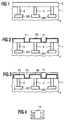
- a substrate 1 comprises the monocrystalline Contains silicon, one selection transistors DRAM cell array, its gate electrodes with word lines (not shown) are connected. On the substrate 1 an insulating layer I deposited in the contacts K too Source / drain regions S / D of the selection transistors generated be (see Figure 1).
- WSi 0.4 is deposited to a thickness of approximately 300 nm to produce a conductive layer L (see FIG. 1).
- a first capacitor electrode P1 arises from the conductive layer L. Flanks of the first capacitor electrode P1 are approximately 300 nm high.
- BST in deposited to a thickness of about 30 nm (see Figure 2).
- second capacitor electrodes P2 To produce second capacitor electrodes P2, WSi 0.4 is deposited in a thickness of 100 nm and planarized by chemical mechanical polishing.
- the second capacitor electrodes P2 form a continuous capacitor plate (see Figure 3).
- the first capacitor electrode P1 ' can be produced, for example, in the form of a crown structure. To enlarge its surface, it can be provided with protuberances, projections or depressions (cf. FIG. 4). Instead of WSi 0.4 , WSi x can be used with 0.3 ⁇ x ⁇ 0.7. WSi x can be nitrided. Instead of BST, other materials can be used for the capacitor dielectric.
- the second capacitor electrodes can be connected to bit lines. In this case, they do not form a continuous capacitor plate.
Landscapes
- Engineering & Computer Science (AREA)
- Manufacturing & Machinery (AREA)
- Semiconductor Memories (AREA)
- Semiconductor Integrated Circuits (AREA)
Abstract
Description


- Figur 1
- zeigt einen Querschnitt durch ein Substrat, das Auswahltransistoren umfaßt, nachdem eine isolierende Schicht, Kontakte und eine erste leitende Schicht erzeugt wurden.
- Figur 2
- zeigt den Schnitt aus Figur 1, nachdem die leitende Schicht strukturiert und ein Kondensatordielektrikum erzeugt wurde.
- Figur 3
- zeigt den Querschnitt aus Figur 2, nachdem eine zweite Kondensatorelektrode erzeugt wurde.
- Figur 4
- zeigt einen Querschnitt durch eine Kondensatorelektrode (P1').
Claims (13)
- Schaltungsanordnung mit mindestens einem Kondensator,bei der mindestens eine Kondensatorelektrode (P1) des Kondensators WSix mit 0,3 < x < 0,7 enthält,bei der ein Kondensatordielektrikum (Kd) des Kondensators ein Ferroelektrikum enthält.
- Schaltungsanordnung nach Anspruch 1,bei dem das Kondensatordielektrikum (Kd) BST enthält.
- Schaltungsanordnung nach Anspruch 1 oder 2,bei der eine Abmessung der Kondensatorelektrode (P1) senkrecht zu einer Oberfläche eines Substrats (1), in dem die Schaltungsanordnung angeordnet ist, größer als etwa 100 nm beträgt.
- Schaltungsanordnung nach Anspruch 3,bei der die Kondensatorelektrode (P1') Ausstülpungen, Vorsprünge und/oder Vertiefungen aufweist.
- Schaltungsanordnung nach einem der Ansprüche 1 bis 4,bei der ein Substrat (1), das die Schaltungsanordnung umfaßt, Silizium enthält.
- Schaltungsanordnung nach einem der Ansprüche 1 bis 5,die eine DRAM-Zellenanordnung ist.
- Verfahren zur Erzeugung einer Schaltungsanordnung mit mindestens einem Kondensator,bei dem mindestens eine Kondensatorelektrode (P1) des Kondensators mindestens teilweise aus WSix mit 0,3 < x < 0,7 erzeugt wird,bei dem ein Kondensatordielektrikum (Kd) des Kondensators erzeugt wird, das ein Ferroelektrikum enthält.
- Verfahren nach Anspruch 7,bei dem das Kondensatordielektrikum (Kd) aus BST erzeugt wird.
- Verfahren nach einem der Ansprüche 7 oder 8,bei dem die Kondensatorelektrode (P1) durch Strukturierung einer leitenden Schicht (L), die dicker als etwa 100nm ist, erzeugt wird.
- Verfahren nach Anspruch 9,bei dem die Kondensatorelektrode (P1) mit Ausstülpungen, Vorsprüngen und/oder Vertiefungen versehen wird.
- Verfahren nach einem der Ansprüche 7 bis 10,bei dem die Schaltungsanordnung in einem Substrat (1) erzeugt wird, das Silizium enthält.
- Verfahren nach einem der Ansprüche 7 bis 11,bei dem die Schaltungsanordnung als eine DRAM-Zellenanordnung erzeugt wird.
- Verfahren nach einem der Ansprüche 7 bis 12,bei dem zur Erzeugung der Kondensatorelektrode (P1) WSix mit 0,3 < x < 0,7 nitridiert wird.
Applications Claiming Priority (2)
| Application Number | Priority Date | Filing Date | Title |
|---|---|---|---|
| DE19806307 | 1998-02-16 | ||
| DE19806307 | 1998-02-16 |
Publications (2)
| Publication Number | Publication Date |
|---|---|
| EP0936678A1 true EP0936678A1 (de) | 1999-08-18 |
| EP0936678B1 EP0936678B1 (de) | 2007-03-21 |
Family
ID=7857861
Family Applications (1)
| Application Number | Title | Priority Date | Filing Date |
|---|---|---|---|
| EP98124017A Expired - Lifetime EP0936678B1 (de) | 1998-02-16 | 1998-12-17 | Schaltungsanordnung mit mindestens einem Kondensator und Verfahren zu deren Herstellung |
Country Status (6)
| Country | Link |
|---|---|
| US (1) | US6359296B1 (de) |
| EP (1) | EP0936678B1 (de) |
| JP (1) | JPH11274417A (de) |
| KR (1) | KR100602289B1 (de) |
| DE (1) | DE59813949D1 (de) |
| TW (1) | TW417279B (de) |
Cited By (2)
| Publication number | Priority date | Publication date | Assignee | Title |
|---|---|---|---|---|
| WO2003075361A3 (en) * | 2002-03-07 | 2003-12-31 | Philips Intellectual Property | Monolithic integrated soi circuit with capacitor |
| WO2004019410A1 (en) * | 2002-08-20 | 2004-03-04 | Koninklijke Philips Electronics N.V. | Ferroelectric device and method of manufacturing such a device |
Families Citing this family (3)
| Publication number | Priority date | Publication date | Assignee | Title |
|---|---|---|---|---|
| DE10022655C2 (de) * | 2000-04-28 | 2002-03-07 | Infineon Technologies Ag | Verfahren zur Herstellung von Kondensatorstrukturen |
| DE10324055B4 (de) * | 2003-05-27 | 2005-10-13 | Texas Instruments Deutschland Gmbh | Verfahren zur Herstellung eines integrierten Stapelkondensators |
| US11101274B2 (en) * | 2019-12-05 | 2021-08-24 | Micron Technology, Inc. | Ferroelectric capacitor, a ferroelectric memory cell, an array of ferroelectric memory cells, and a method of forming a ferroelectric capacitor |
Citations (6)
| Publication number | Priority date | Publication date | Assignee | Title |
|---|---|---|---|---|
| EP0412185A1 (de) * | 1989-08-09 | 1991-02-13 | Siemens Aktiengesellschaft | Metallisierung mit Diffusionsbarriere für Halbleiterbauelemente |
| DE4300808C1 (de) * | 1993-01-14 | 1994-03-17 | Siemens Ag | Verfahren zur Herstellung eines Vielschichtkondensators |
| JPH0817822A (ja) * | 1994-06-27 | 1996-01-19 | Nec Corp | 半導体装置およびその製造方法 |
| EP0697720A1 (de) * | 1994-08-01 | 1996-02-21 | Texas Instruments Incorporated | Leitfähige Barriereschicht aus einem amorphen Nitrid als Elektrode für Material mit hoher dielektrischen Konstante |
| EP0722190A2 (de) * | 1995-01-12 | 1996-07-17 | International Business Machines Corporation | TaSiN-Sauerstoff-Diffusionsbarriere in Mehrschichtstrukturen |
| US5566045A (en) * | 1994-08-01 | 1996-10-15 | Texas Instruments, Inc. | High-dielectric-constant material electrodes comprising thin platinum layers |
Family Cites Families (6)
| Publication number | Priority date | Publication date | Assignee | Title |
|---|---|---|---|---|
| US5382817A (en) * | 1992-02-20 | 1995-01-17 | Mitsubishi Denki Kabushiki Kaisha | Semiconductor device having a ferroelectric capacitor with a planarized lower electrode |
| JP2897631B2 (ja) * | 1993-12-28 | 1999-05-31 | 日本電気株式会社 | 半導体集積回路装置および製造方法 |
| KR970018748A (ko) * | 1995-09-29 | 1997-04-30 | 김광호 | 강유전체 커패시터의 제조방법 |
| KR970024140A (ko) * | 1995-10-11 | 1997-05-30 | 김광호 | 강유전체 커패시터를 가지는 반도체 장치 |
| KR100191780B1 (ko) * | 1995-12-23 | 1999-06-15 | 윤종용 | 반도체 장치의 커패시터 및 그 제조방법 |
| KR100230422B1 (ko) * | 1997-04-25 | 1999-11-15 | 윤종용 | 반도체장치의 커패시터 제조방법 |
-
1998
- 1998-12-17 EP EP98124017A patent/EP0936678B1/de not_active Expired - Lifetime
- 1998-12-17 DE DE59813949T patent/DE59813949D1/de not_active Expired - Fee Related
-
1999
- 1999-01-14 TW TW088100511A patent/TW417279B/zh not_active IP Right Cessation
- 1999-02-11 KR KR1019990004809A patent/KR100602289B1/ko not_active Expired - Fee Related
- 1999-02-15 JP JP11036038A patent/JPH11274417A/ja active Pending
- 1999-02-16 US US09/250,516 patent/US6359296B1/en not_active Expired - Lifetime
Patent Citations (6)
| Publication number | Priority date | Publication date | Assignee | Title |
|---|---|---|---|---|
| EP0412185A1 (de) * | 1989-08-09 | 1991-02-13 | Siemens Aktiengesellschaft | Metallisierung mit Diffusionsbarriere für Halbleiterbauelemente |
| DE4300808C1 (de) * | 1993-01-14 | 1994-03-17 | Siemens Ag | Verfahren zur Herstellung eines Vielschichtkondensators |
| JPH0817822A (ja) * | 1994-06-27 | 1996-01-19 | Nec Corp | 半導体装置およびその製造方法 |
| EP0697720A1 (de) * | 1994-08-01 | 1996-02-21 | Texas Instruments Incorporated | Leitfähige Barriereschicht aus einem amorphen Nitrid als Elektrode für Material mit hoher dielektrischen Konstante |
| US5566045A (en) * | 1994-08-01 | 1996-10-15 | Texas Instruments, Inc. | High-dielectric-constant material electrodes comprising thin platinum layers |
| EP0722190A2 (de) * | 1995-01-12 | 1996-07-17 | International Business Machines Corporation | TaSiN-Sauerstoff-Diffusionsbarriere in Mehrschichtstrukturen |
Non-Patent Citations (3)
| Title |
|---|
| PATENT ABSTRACTS OF JAPAN vol. 096, no. 005 31 May 1996 (1996-05-31) * |
| REID J S ET AL: "EVALUATION OF AMORPHOUS (MO,TA,W)-SI-N DIFFUSION BARRIERS FOR (SI)/CU METALLIZATIONS", THIN SOLID FILMS, vol. 236, no. 1/02, 15 December 1993 (1993-12-15), pages 319 - 324, XP000415529 * |
| SHIMOOKA Y ET AL: "CORRELATION OF W-SI-N FILM MICROSTRUCTURE WITH BARRIER PERFORMANCE AGAINST CU DIFFUSION", JAPANESE JOURNAL OF APPLIED PHYSICS, vol. 36, no. 3B, PART 01, March 1997 (1997-03-01), pages 1589 - 1592, XP000703083 * |
Cited By (3)
| Publication number | Priority date | Publication date | Assignee | Title |
|---|---|---|---|---|
| WO2003075361A3 (en) * | 2002-03-07 | 2003-12-31 | Philips Intellectual Property | Monolithic integrated soi circuit with capacitor |
| CN100379030C (zh) * | 2002-03-07 | 2008-04-02 | Nxp股份有限公司 | 具有电容器的单片集成soi电路 |
| WO2004019410A1 (en) * | 2002-08-20 | 2004-03-04 | Koninklijke Philips Electronics N.V. | Ferroelectric device and method of manufacturing such a device |
Also Published As
| Publication number | Publication date |
|---|---|
| TW417279B (en) | 2001-01-01 |
| KR19990072587A (ko) | 1999-09-27 |
| EP0936678B1 (de) | 2007-03-21 |
| DE59813949D1 (de) | 2007-05-03 |
| JPH11274417A (ja) | 1999-10-08 |
| KR100602289B1 (ko) | 2006-07-14 |
| US6359296B1 (en) | 2002-03-19 |
Similar Documents
| Publication | Publication Date | Title |
|---|---|---|
| DE69113579T2 (de) | Verfahren zur Herstellung einer DRAM-Zelle mit Stapelkondensator. | |
| DE3851163T2 (de) | Kontakt in einer Bohrung in einem Halbleiter und Verfahren zu seiner Herstellung. | |
| DE3141195C2 (de) | ||
| DE19860829B4 (de) | Verfahren zur Herstellung eines Halbleiterbausteins | |
| DE19930295C2 (de) | Säulenförmiger Speicherknoten eines Kondensators und Verfahren zur Herstellung desselben | |
| EP0744772A1 (de) | DRAM-Speicherzelle mit vertikalem Transistor und Verfahren zur Herstellung derselben | |
| DE69315125T2 (de) | Herstellungsverfahren für Halbleiterbauelement mit Kondensator | |
| DE3906874A1 (de) | Kondensator und verfahren zu dessen herstellung | |
| WO2000013224A1 (de) | Mikroelektronische struktur, verfahren zu deren herstellung und deren verwendung in einer speicherzelle | |
| DE19649670C2 (de) | Verfahren zur Herstellung eines Kondensators einer Halbleitervorrichtung und auf diese Weise hergestellter Kondensator | |
| DE4232817B4 (de) | Halbleiter-Speicherzelle und Verfahren zu deren Herstellung | |
| EP1145319B1 (de) | Integrierte schaltungsanordnung und verfahren zu deren herstellung | |
| DE3918924A1 (de) | Halbleiterspeichereinrichtung vom gestapelten kondensatortyp und herstellungsverfahren dafuer | |
| DE3877282T2 (de) | Verfahren zum herstellen einer halbleiter-vorrichtung. | |
| DE10109564A1 (de) | Grabenkondensator und Verfahren zu seiner Herstellung | |
| DE19822048A1 (de) | Verfahren zum Ätzen von Tantaloxidschichten | |
| DE19712540C1 (de) | Herstellverfahren für eine Kondensatorelektrode aus einem Platinmetall | |
| EP0862207A1 (de) | Verfahren zur Herstellung eines DRAM-Grabenkondensators | |
| EP0936678B1 (de) | Schaltungsanordnung mit mindestens einem Kondensator und Verfahren zu deren Herstellung | |
| DE19950540B4 (de) | Verfahren zur Herstellung einer Kondensator-Elektrode mit Barrierestruktur | |
| DE19620185A1 (de) | Verfahren zur Herstellung eines Kondensators einer Halbleitereinrichtung | |
| DE4200284C2 (de) | Halbleitereinrichtung und Verfahren zu deren Herstellung | |
| EP1364408B1 (de) | Verfahrenher zur herstellung einer elektrodenanordnung zur ladungsspeicherung | |
| EP0987756A2 (de) | Gestapelter Flossenkondensator für DRAM und Verfahren zur Herstellung desselben | |
| EP1222695B1 (de) | Integrierte schaltungsanordnung mit mindestens einem kondensator und verfahren zu deren herstellung |
Legal Events
| Date | Code | Title | Description |
|---|---|---|---|
| PUAI | Public reference made under article 153(3) epc to a published international application that has entered the european phase |
Free format text: ORIGINAL CODE: 0009012 |
|
| AK | Designated contracting states |
Kind code of ref document: A1 Designated state(s): DE FR GB IE IT |
|
| AX | Request for extension of the european patent |
Free format text: AL;LT;LV;MK;RO;SI |
|
| RTI1 | Title (correction) |
Free format text: CIRCUIT STRUCTURE WITH AT LEAST ONE CAPACITOR AND CORRESPONDING METHOD |
|
| 17P | Request for examination filed |
Effective date: 19990903 |
|
| AKX | Designation fees paid |
Free format text: DE FR GB IE IT |
|
| RAP1 | Party data changed (applicant data changed or rights of an application transferred) |
Owner name: INFINEON TECHNOLOGIES AG |
|
| GRAP | Despatch of communication of intention to grant a patent |
Free format text: ORIGINAL CODE: EPIDOSNIGR1 |
|
| GRAS | Grant fee paid |
Free format text: ORIGINAL CODE: EPIDOSNIGR3 |
|
| GRAA | (expected) grant |
Free format text: ORIGINAL CODE: 0009210 |
|
| AK | Designated contracting states |
Kind code of ref document: B1 Designated state(s): DE FR GB IE IT |
|
| PG25 | Lapsed in a contracting state [announced via postgrant information from national office to epo] |
Ref country code: IE Free format text: LAPSE BECAUSE OF FAILURE TO SUBMIT A TRANSLATION OF THE DESCRIPTION OR TO PAY THE FEE WITHIN THE PRESCRIBED TIME-LIMIT Effective date: 20070321 |
|
| REG | Reference to a national code |
Ref country code: GB Ref legal event code: FG4D Free format text: NOT ENGLISH |
|
| REF | Corresponds to: |
Ref document number: 59813949 Country of ref document: DE Date of ref document: 20070503 Kind code of ref document: P |
|
| REG | Reference to a national code |
Ref country code: IE Ref legal event code: FG4D Free format text: LANGUAGE OF EP DOCUMENT: GERMAN |
|
| GBV | Gb: ep patent (uk) treated as always having been void in accordance with gb section 77(7)/1977 [no translation filed] |
Effective date: 20070321 |
|
| REG | Reference to a national code |
Ref country code: IE Ref legal event code: FD4D |
|
| EN | Fr: translation not filed | ||
| PG25 | Lapsed in a contracting state [announced via postgrant information from national office to epo] |
Ref country code: GB Free format text: LAPSE BECAUSE OF FAILURE TO SUBMIT A TRANSLATION OF THE DESCRIPTION OR TO PAY THE FEE WITHIN THE PRESCRIBED TIME-LIMIT Effective date: 20070321 |
|
| PLBE | No opposition filed within time limit |
Free format text: ORIGINAL CODE: 0009261 |
|
| STAA | Information on the status of an ep patent application or granted ep patent |
Free format text: STATUS: NO OPPOSITION FILED WITHIN TIME LIMIT |
|
| 26N | No opposition filed |
Effective date: 20071227 |
|
| PG25 | Lapsed in a contracting state [announced via postgrant information from national office to epo] |
Ref country code: IT Free format text: LAPSE BECAUSE OF FAILURE TO SUBMIT A TRANSLATION OF THE DESCRIPTION OR TO PAY THE FEE WITHIN THE PRESCRIBED TIME-LIMIT Effective date: 20070321 Ref country code: FR Free format text: LAPSE BECAUSE OF FAILURE TO SUBMIT A TRANSLATION OF THE DESCRIPTION OR TO PAY THE FEE WITHIN THE PRESCRIBED TIME-LIMIT Effective date: 20071123 |
|
| PGFP | Annual fee paid to national office [announced via postgrant information from national office to epo] |
Ref country code: DE Payment date: 20080213 Year of fee payment: 10 |
|
| PG25 | Lapsed in a contracting state [announced via postgrant information from national office to epo] |
Ref country code: FR Free format text: LAPSE BECAUSE OF FAILURE TO SUBMIT A TRANSLATION OF THE DESCRIPTION OR TO PAY THE FEE WITHIN THE PRESCRIBED TIME-LIMIT Effective date: 20070321 |
|
| PG25 | Lapsed in a contracting state [announced via postgrant information from national office to epo] |
Ref country code: DE Free format text: LAPSE BECAUSE OF NON-PAYMENT OF DUE FEES Effective date: 20090701 |