EP0936695B1 - Antenne semi-conducteur à balayage électronique - Google Patents
Antenne semi-conducteur à balayage électronique Download PDFInfo
- Publication number
- EP0936695B1 EP0936695B1 EP99102592A EP99102592A EP0936695B1 EP 0936695 B1 EP0936695 B1 EP 0936695B1 EP 99102592 A EP99102592 A EP 99102592A EP 99102592 A EP99102592 A EP 99102592A EP 0936695 B1 EP0936695 B1 EP 0936695B1
- Authority
- EP
- European Patent Office
- Prior art keywords
- antenna
- semiconductor substrate
- array
- antenna apparatus
- stubs
- Prior art date
- Legal status (The legal status is an assumption and is not a legal conclusion. Google has not performed a legal analysis and makes no representation as to the accuracy of the status listed.)
- Expired - Lifetime
Links
Images

Classifications
-
- H—ELECTRICITY
- H01—ELECTRIC ELEMENTS
- H01Q—ANTENNAS, i.e. RADIO AERIALS
- H01Q13/00—Waveguide horns or mouths; Slot antennas; Leaky-waveguide antennas; Equivalent structures causing radiation along the transmission path of a guided wave
- H01Q13/20—Non-resonant leaky-waveguide or transmission-line antennas; Equivalent structures causing radiation along the transmission path of a guided wave
- H01Q13/28—Non-resonant leaky-waveguide or transmission-line antennas; Equivalent structures causing radiation along the transmission path of a guided wave comprising elements constituting electric discontinuities and spaced in direction of wave propagation, e.g. dielectric elements or conductive elements forming artificial dielectric
-
- H—ELECTRICITY
- H01—ELECTRIC ELEMENTS
- H01Q—ANTENNAS, i.e. RADIO AERIALS
- H01Q13/00—Waveguide horns or mouths; Slot antennas; Leaky-waveguide antennas; Equivalent structures causing radiation along the transmission path of a guided wave
- H01Q13/20—Non-resonant leaky-waveguide or transmission-line antennas; Equivalent structures causing radiation along the transmission path of a guided wave
-
- H—ELECTRICITY
- H01—ELECTRIC ELEMENTS
- H01Q—ANTENNAS, i.e. RADIO AERIALS
- H01Q3/00—Arrangements for changing or varying the orientation or the shape of the directional pattern of the waves radiated from an antenna or antenna system
- H01Q3/26—Arrangements for changing or varying the orientation or the shape of the directional pattern of the waves radiated from an antenna or antenna system varying the relative phase or relative amplitude of energisation between two or more active radiating elements; varying the distribution of energy across a radiating aperture
- H01Q3/30—Arrangements for changing or varying the orientation or the shape of the directional pattern of the waves radiated from an antenna or antenna system varying the relative phase or relative amplitude of energisation between two or more active radiating elements; varying the distribution of energy across a radiating aperture varying the relative phase between the radiating elements of an array
- H01Q3/34—Arrangements for changing or varying the orientation or the shape of the directional pattern of the waves radiated from an antenna or antenna system varying the relative phase or relative amplitude of energisation between two or more active radiating elements; varying the distribution of energy across a radiating aperture varying the relative phase between the radiating elements of an array by electrical means
- H01Q3/36—Arrangements for changing or varying the orientation or the shape of the directional pattern of the waves radiated from an antenna or antenna system varying the relative phase or relative amplitude of energisation between two or more active radiating elements; varying the distribution of energy across a radiating aperture varying the relative phase between the radiating elements of an array by electrical means with variable phase-shifters
Definitions
- the present invention relates generally to electronically scanned antennas, and more particularly, to an electronically scanned semiconductor antenna.
- US 5 469 165 A discloses a radar and electronic warfare system comprising a variety of continuous transverse stub antenna arrays combined with a radar and electronic warfare subsystem.
- the radar system uses a voltage variable dielectric continuous transverse stub antenna array to form a continuous transverse stub electronically scanned radar system.
- a high voltage power supply is used to electronically steer the continuous transverse stub antenna array in the E-plane (perpendicular to the direction of the stubs).
- a beam steering computer is used to set phase shifters to steer the beam in the H-plane to a desired pointing angle. This system provides for two dimensional electronic scanning of the continuous transverse stub antenna array.
- US 4 320 404 A discloses a microwave phase shifter and its application to electronic scanning.
- a plurality of metallic wire conductors are fitted in shunt along a shorted waveguide parallel to a dielectric field of electromagnetic wave incident to the waveguide.
- At least some of the wires have diodes mounted on them such that selective biasing of the diodes renders these wires discontinuous and causes a controlled phase shift of the incident wave.
- the present invention provides for an electronically scanned semiconductor antenna that is manufactured using conventional semiconductor device fabrication technology.
- the antenna is fashioned in the form of a continuous transverse stub array geometry but uses a semiconductor substrate, such as silicon, gallium arsenide, or indium phosphide, for example.
- the antenna has a semiconductor substrate having a plurality of stubs projecting from one surface.
- the semiconductor substrate may be silicon, gallium arsenide, or indium phosphide, for example.
- a first conductive layer formed on the surfaces of the semiconductor substrate and along sides of the stubs so that the stubs are open at their terminus.
- the conductive layers form a parallel plate waveguide region.
- a diode array having a plurality of diode elements is formed in the semiconductor substrate that are disposed transversely across the semiconductor substrate and longitudinally down the semiconductor substrate between selected ones of the plurality of stubs.
- the diode array provides a voltage variable capacitive reactance in selective regions of the waveguide region.
- a beam steering computer is coupled to the plurality of diode elements of the diode array which controls the voltage applied thereto to control steering of a beam radiated by the antenna.
- the electromagnetic energy is launched from one end of the array and selectively coupled into the transverse stubs.
- the radiation pattern is set by the dimensions of transverse stubs projecting from the substrate relative to a parallel plate waveguide region and the free space wavelength, I 0 , as it pertains to the element spacing.
- a continuous or discrete pattern of Schottky diodes or PN-junction varactor diodes is fabricated in the semiconductor substrate. The voltage variable capacitance of these simple elements is used to cause a phase shift as the energy propagates between the stub radiators. This phase shift results in the two-dimensional scanning of an antenna beam pattern produced by the antenna.
- the novelty of the present invention involves the use of the Schottky or varactor diode pattern within the transmission medium, and the use of a semiconductor transmission medium for the antenna. Since a Schottky junction is a metal-semiconductor junction, fabrication costs are low. The radiation elements and the precise location of the elements is achieved using conventional photolithographic techniques and active device geometry is easily achieved compared to transistor (HEMT, FET, HBT, and bipolar) designs.
- the present antenna provides the ability to cost effectively manufacture electronically scanned arrays in the millimeter-wave bands.
- the present invention provides an antenna for use in small diameter, millimeter-wave, active radar sensor missiles, collision avoidance radars for automobiles and other vehicles, and millimeter-wave communication links for use on satellites.
- the present electronically scanned semiconductor antenna provides a feasible and practical means for achieving two-dimensional electronic radiation pattern scanning for millimeter-wave radars that are confined to small apertures.
- the present antenna provides two-dimensional scanning capability and takes advantage of existing semiconductor material fabrication technology. Since the preferable material of choice for use in the present antenna is silicon, the insertion loss of the antenna should be very low compared to other more exotic materials.
- this present invention incorporates the scanning mechanism directly in the bulk semiconductor antenna. Using the precision of monolithic microwave integrated circuit fabrication techniques, element spacing and antenna geometry may be realized in a cost effective manner. Beam steering control line packaging is considerably simplified using readily-available LSI packaging techniques.
- Fig. 1 illustrates a conventional continuous transverse stub array antenna 10 developed by the assignee of the present invention.
- the present invention builds upon the geometry of the continuous transverse stub array antenna 10 developed by the assignee of the present invention.
- the present invention incorporates a unique technology and mechanization to provide a two-dimensional electronic scan mechanism for microwave and millimeter-wave antennas.
- the continuous transverse stub antenna 10 is fabricated from conventional dielectric material 13, usually a plastic material, such as Rexolite, for example. Top and bottom surfaces 11, 12 of the antenna 10 are plated with conductive material to form a parallel plate waveguide medium that provides a feed system 14 for energy propagation. Parallel plate waveguide stubs 15 are oriented transverse to the parallel plate feed system 14, plated on the sides, but open at their terminus. The propagating wave in the feed system 14 encounters transverse stubs 15 which couple off energy in a prescribed manner to achieve the desired radiation pattern of the antenna 10.
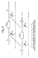
- Fig. 2 it illustrates a portion of an electronically scanned semiconductor antenna 20 in accordance with the principles of the present invention which improves upon the array of Fig. 1.
- the geometry of the continuous transverse stub antenna 10 is used in the present antenna 20, except that the present antenna 20 is fabricated using an appropriate bulk semiconductor material as a substrate 13.
- the semiconductor material may include silicon, gallium arsenide, and indium phosphide, for example. Silicon is believed to be the most cost effective material of choice, given the maturity of silicon technology used in the computer industry.
- transverse stubs 15 comprised of semiconductor material project from the surface of the semiconductor wafer.
- Plating material (the majority of which is shown removed to expose the underlying semiconductor material) covers the top and bottom surfaces 11, 12 to establish the parallel plate waveguide region 14.
- Ridges 15 or stubs 15 are fabricated using photolithographic and semiconductor etching techniques. In the open areas between the ridges 15, the plating material or semiconductor doping is controlled so as to fabricate a Schottky or varactor diode array 21 in a discrete or continuous sense across and down the propagation medium comprising the semiconductor material.
- the Schottky or varactor diode array 21 provides a voltage variable capacitive reactance in selective regions across the waveguide region 14. The voltage variable capacitive reactance provides a means to shift the phase of the incident energy, which was launched into the waveguide region.
- this arrangement of diode arrays 21 provides for a set of voltage variable, distributed filter and phase shifter networks cascaded down and across the parallel plate waveguide region 14 which forms a transmission line.
- Schottky diodes employ a metal contacted to an N-type semiconductor. N-type semiconductor and p-type doping provide a suitable propagation medium. Additionally, both Schottky and varactor diodes exhibit a continuous capacitance versus voltage characteristic which provides a continuous reactance control feature. The reverse bias nature of the devices requires literally no control current (typically microamperes) only a voltage change; this feature makes control of the diode array 21 convenient and easy to accomplish. Furthermore the diode arrays 21 have an exceptionally fast response time (nanoseconds). The diode arrays 21 require voltages no larger than 40 volts, and thus no high voltage power supply is required.
- a canted transverse phase front provides an H-plane scan mechanism.
- the phase shift can be adjusted in both the transverse and longitudinal axis to affect both the E- and H-plane scanning mechanisms.
- a two-dimensional passive electronic scan is provided by the present antenna 20.
- a line of individual Schottky or varactor diodes 21 across the width of the antenna 20 (transverse axis) independent voltage controlled, localized reactance is encountered by the propagating energy in the transverse plane.
- This single line of diode arrays 21 cause varying localized phase shifts across the arrays 21 at the point of the line feed. The result is the canting of the phase front and therefore scanning of the beam in the H-plane.
- the Schottky and varactor diode arrays 21 are fabricated as either a discrete or continuous linear region parallel to the stubs but cascaded down the longitudinal axis of the arrays 21, the propagating wave encounters uniform reactance networks transverse to the direction of energy propagation.
- the resultant phase shift may be controlled to provide the E-plane beam scan in the cross dimension.
- the effective longitudinal electrical length of the antenna 20 is changed and is continuously variable.
- the beam By varying the voltage across for a first line of diode arrays 21, the beam scans in the H-plane. By varying the voltage down the diode arrays 21, the beam scans in the E-plane.
- the continuous variable reactance feature with low voltage provides continuous beam steering control. Multiple diode arrays 21 and values are appropriately selected and designed to provide adequate input impedance matching at the line feed input.
- diode arrays 21 using such techniques as molecular beam epitaxy or ion beam implantation is simple compared to the complex monolithic microwave integrated circuits built by the assignee of the present invention. Precise location, doping profiles and circuit interconnection are readily available; some oxide layers may be employed to achieve isolated bias lines. Beam steering control pads may be placed along edges of the antenna 20 for coupling to a beam steering computer 25. High rate interconnect technology applies directly. Only low voltage power supplies with little current requirement are needed.
- the radiator element (stub 15 or ridge 15) spacing is less than 0.15 cm (0.060").
- Conventional phased array technology is not feasible from a packaging geometry perspective.
- the present invention is ideal for small aperture 5.08-7.62 cm (2-3 inch)diameter) applications where electronic two-dimensional scanning is required.
- Silicon wafer fabrication sizes, available with today's reactor sizes for high rate computer chip production, provide significant antenna gains at the millimeter-wave frequencies.
- the present invention thus provides a cost effective option for two-dimensional electronically scanned millimeter-wave antennas, heretofore, not available.
- the present invention relates to an electronically scanned antenna 20 that is manufactured using semiconductor material and device fabrication technology.
- the antenna 20 has a semiconductor substrate 13 having a plurality of stubs 15 projecting from one surface.
- the semiconductor substrate may be silicon, gallium arsenide, or indium phosphide, for example.
- a first conductive layer 11 formed on the surfaces of the semiconductor substrate 13 and along sides of the stubs so that the stubs 15 are open at their terminus.
- the conductive layers 11, 12 form a parallel plate waveguide region 14.
- a diode array 21 having a plurality of diode elements is formed in the semiconductor substrate 13 that are disposed transversely across the semiconductor substrate 13 and longitudinally down the semiconductor substrate 13 between selected ones of the plurality of stubs 15.
- the diode array 21 may comprise an array of Schottky or varactor diodes, for example.
- the diode array 21 provides a voltage variable capacitive reactance in selective regions of the waveguide region 14.
- a beam steering computer 25 is coupled to the plurality of diode elements of the diode array 21 which controls the voltage applied thereto to control steering of a beam radiated by the antenna 20.
Landscapes
- Variable-Direction Aerials And Aerial Arrays (AREA)
Claims (8)
- Structure d'antenne (20) comprenant :un substrat (13) ayant une première surface et une seconde surface ayant une pluralité de tronçons (15) faisant saillie à partir de cette dernière;une première couche conductrice (11) formée sur la première surface du substrat (13),une seconde couche conductrice (12) formée sur la seconde surface du substrat (13) et le long de côtés de la pluralité de tronçons faisant saillie à partir du substrat (13), de façon que les tronçons (15) soient ouverts à leur extrémité terminale, et dans laquelle les première et seconde couches conductrices (11, 12) forment une région de guide d'ondes à plaques parallèles (14); caractérisée en ce quele substrat (13) est un substrat semiconducteur (13), etun réseau de diodes (21) est incorporé et il comprend une pluralité d'éléments consistant en diodes formés dans le substrat semiconducteur (13) qui sont disposés transversalement au substrat semiconducteur (13) et dans la direction longitudinale du substrat semiconducteur (13) entre des tronçons sélectionnés de la pluralité de tronçons (15), ce réseau de diodes (21) procurant une réactance capacitive variable en fonction de la tension, dans des régions sélectives de la région de guide d'ondes (14).
- Structure d'antenne (20) selon la revendication 1, caractérisée en ce que la pluralité d'éléments consistant en diodes du réseau de diodes (21) sont couplés à un ordinateur de pointage de faisceau (25) qui commande la tension qui leur est appliquée, pour commander le pointage d'un faisceau rayonné par l'antenne (20).
- Structure d'antenne (20) selon la revendication 1 ou 2, caractérisée en ce que le réseau de diodes (21) comprend un réseau de diodes Schottky.
- Structure d'antenne (20) selon la revendication 1 ou 2, caractérisée en ce que le réseau de diodes (21) comprend un réseau de diodes de type varactor.
- Structure d'antenne (20) selon l'une quelconque des revendications 1 à 4, caractérisée en ce que le substrat semiconducteur (13) consiste en silicium.
- Structure d'antenne (20) selon l'une quelconque des revendications 1 à 4, caractérisée en ce que le substrat semiconducteur (13) consiste en arséniure de gallium.
- Structure d'antenne (20) selon l'une quelconque des revendications 1 à 4, caractérisée en ce que le substrat semiconducteur (13) consiste en phosphure d'indium.
- Structure d'antenne selon l'une quelconque des revendications précédentes, caractérisée en ce qu'elle consiste en une antenne à balayage électronique (20).
Applications Claiming Priority (2)
| Application Number | Priority Date | Filing Date | Title |
|---|---|---|---|
| US23450 | 1987-03-09 | ||
| US09/023,450 US6064349A (en) | 1998-02-13 | 1998-02-13 | Electronically scanned semiconductor antenna |
Publications (2)
| Publication Number | Publication Date |
|---|---|
| EP0936695A1 EP0936695A1 (fr) | 1999-08-18 |
| EP0936695B1 true EP0936695B1 (fr) | 2002-08-14 |
Family
ID=21815190
Family Applications (1)
| Application Number | Title | Priority Date | Filing Date |
|---|---|---|---|
| EP99102592A Expired - Lifetime EP0936695B1 (fr) | 1998-02-13 | 1999-02-11 | Antenne semi-conducteur à balayage électronique |
Country Status (3)
| Country | Link |
|---|---|
| US (2) | US6064349A (fr) |
| EP (1) | EP0936695B1 (fr) |
| DE (1) | DE69902490T2 (fr) |
Families Citing this family (13)
| Publication number | Priority date | Publication date | Assignee | Title |
|---|---|---|---|---|
| USRE43699E1 (en) | 2002-02-05 | 2012-10-02 | Theodore R. Anderson | Reconfigurable scanner and RFID system using the scanner |
| US6700544B2 (en) | 2002-02-05 | 2004-03-02 | Theodore R. Anderson | Near-field plasma reader |
| US6975267B2 (en) * | 2003-02-05 | 2005-12-13 | Northrop Grumman Corporation | Low profile active electronically scanned antenna (AESA) for Ka-band radar systems |
| US6999040B2 (en) * | 2003-06-18 | 2006-02-14 | Raytheon Company | Transverse device array phase shifter circuit techniques and antennas |
| WO2005043180A2 (fr) * | 2003-10-21 | 2005-05-12 | University Of Delaware | Procedes et appareil de detection d'ondes |
| US7079082B2 (en) * | 2004-03-31 | 2006-07-18 | University Of Hawaii | Coplanar waveguide continuous transverse stub (CPW-CTS) antenna for wireless communications |
| US7061443B2 (en) * | 2004-04-01 | 2006-06-13 | Raytheon Company | MMW electronically scanned antenna |
| US20060044189A1 (en) * | 2004-09-01 | 2006-03-02 | Livingston Stan W | Radome structure |
| US7106265B2 (en) * | 2004-12-20 | 2006-09-12 | Raytheon Company | Transverse device array radiator ESA |
| US8279129B1 (en) | 2007-12-21 | 2012-10-02 | Raytheon Company | Transverse device phase shifter |
| US8098207B1 (en) * | 2008-09-16 | 2012-01-17 | Rockwell Collins, Inc. | Electronically scanned antenna |
| KR101182425B1 (ko) * | 2008-12-22 | 2012-09-12 | 한국전자통신연구원 | 스터브가 있는 슬롯 안테나 |
| FR3135572B1 (fr) * | 2022-05-11 | 2024-11-15 | Commissariat Energie Atomique | Antenne faible profil à balayage electronique bidimensionnel |
Family Cites Families (11)
| Publication number | Priority date | Publication date | Assignee | Title |
|---|---|---|---|---|
| US3882431A (en) * | 1973-08-10 | 1975-05-06 | Us Navy | Digital phase shifter |
| FR2412960A1 (fr) * | 1977-12-20 | 1979-07-20 | Radant Etudes | Dephaseur hyperfrequence et son application au balayage electronique |
| US4382261A (en) * | 1980-05-05 | 1983-05-03 | The United States Of America As Represented By The Secretary Of The Army | Phase shifter and line scanner for phased array applications |
| US4575727A (en) * | 1983-06-20 | 1986-03-11 | The United States Of America As Represented By The Secretary Of The Army | Monolithic millimeter-wave electronic scan antenna using Schottky barrier control and method for making same |
| US5266961A (en) * | 1991-08-29 | 1993-11-30 | Hughes Aircraft Company | Continuous transverse stub element devices and methods of making same |
| US5583524A (en) * | 1993-08-10 | 1996-12-10 | Hughes Aircraft Company | Continuous transverse stub element antenna arrays using voltage-variable dielectric material |
| US5483248A (en) * | 1993-08-10 | 1996-01-09 | Hughes Aircraft Company | Continuous transverse stub element devices for flat plate antenna arrays |
| US5469165A (en) * | 1993-12-23 | 1995-11-21 | Hughes Aircraft Company | Radar and electronic warfare systems employing continuous transverse stub array antennas |
| US5652596A (en) * | 1995-09-22 | 1997-07-29 | Hughes Electronics | Scanned antenna system and method |
| US5604505A (en) * | 1996-02-26 | 1997-02-18 | Hughes Electronics | Phase tuning technique for a continuous transverse stub antenna array |
| US5995055A (en) * | 1997-06-30 | 1999-11-30 | Raytheon Company | Planar antenna radiating structure having quasi-scan, frequency-independent driving-point impedance |
-
1998
- 1998-02-13 US US09/023,450 patent/US6064349A/en not_active Expired - Lifetime
-
1999
- 1999-02-11 EP EP99102592A patent/EP0936695B1/fr not_active Expired - Lifetime
- 1999-02-11 DE DE69902490T patent/DE69902490T2/de not_active Expired - Lifetime
- 1999-10-12 US US09/416,138 patent/US6157347A/en not_active Expired - Lifetime
Also Published As
| Publication number | Publication date |
|---|---|
| DE69902490D1 (de) | 2002-09-19 |
| US6064349A (en) | 2000-05-16 |
| US6157347A (en) | 2000-12-05 |
| EP0936695A1 (fr) | 1999-08-18 |
| DE69902490T2 (de) | 2003-04-24 |
Similar Documents
| Publication | Publication Date | Title |
|---|---|---|
| EP1831958B1 (fr) | Antenne a exploration electronique equipee d'elements rayonnants qui forment un reseau de dispositifs transversaux | |
| US7307596B1 (en) | Low-cost one-dimensional electromagnetic band gap waveguide phase shifter based ESA horn antenna | |
| US6806846B1 (en) | Frequency agile material-based reflectarray antenna | |
| US6995726B1 (en) | Split waveguide phased array antenna with integrated bias assembly | |
| US4442590A (en) | Monolithic microwave integrated circuit with integral array antenna | |
| US7151507B1 (en) | Low-loss, dual-band electromagnetic band gap electronically scanned antenna utilizing frequency selective surfaces | |
| KR100655823B1 (ko) | 콤팩트 cts 피드 및 mems 위상 시프터를 갖는광대역 2차원 전자 주사 어레이 | |
| USRE32369E (en) | Monolithic microwave integrated circuit with integral array antenna | |
| US4490721A (en) | Monolithic microwave integrated circuit with integral array antenna | |
| US6999040B2 (en) | Transverse device array phase shifter circuit techniques and antennas | |
| US6597327B2 (en) | Reconfigurable adaptive wideband antenna | |
| US6064349A (en) | Electronically scanned semiconductor antenna | |
| EP0528423A1 (fr) | Dispositif récepteur | |
| EP0055324B1 (fr) | Circuit intégré monolithique à micro-onde avec assemblage d'antenne intégral | |
| US5995055A (en) | Planar antenna radiating structure having quasi-scan, frequency-independent driving-point impedance | |
| CN111106451A (zh) | 一种一维电控波束扫描圆极化天线及其控制方法 | |
| CN110165406B (zh) | 一种方向图可重构天线单元及相控阵 | |
| US7639197B1 (en) | Stacked dual-band electromagnetic band gap waveguide aperture for an electronically scanned array | |
| Chen et al. | Studies of suppression of the reflected wave and beam-scanning features of the antenna arrays | |
| US11888223B2 (en) | Steerable beam antenna | |
| US12527109B2 (en) | Optical control switch and electronic device comprising same | |
| US7688269B1 (en) | Stacked dual-band electromagnetic band gap waveguide aperture with independent feeds | |
| Joseph et al. | Antenna array and GaAs phase shifter MMIC for millimeter wave beamforming-co-simulation and measurements | |
| McSpadden et al. | Ka-band beam steering reflectarray study | |
| Attia | Fabry-Perot Resonant Cavity Antenna with Tunable Superstrate for Beam Steering Millimeter-Wave Applications |
Legal Events
| Date | Code | Title | Description |
|---|---|---|---|
| PUAI | Public reference made under article 153(3) epc to a published international application that has entered the european phase |
Free format text: ORIGINAL CODE: 0009012 |
|
| AK | Designated contracting states |
Kind code of ref document: A1 Designated state(s): DE FR GB NL |
|
| AX | Request for extension of the european patent |
Free format text: AL;LT;LV;MK;RO;SI |
|
| 17P | Request for examination filed |
Effective date: 20000209 |
|
| AKX | Designation fees paid |
Free format text: DE FR GB NL |
|
| GRAG | Despatch of communication of intention to grant |
Free format text: ORIGINAL CODE: EPIDOS AGRA |
|
| 17Q | First examination report despatched |
Effective date: 20011228 |
|
| GRAG | Despatch of communication of intention to grant |
Free format text: ORIGINAL CODE: EPIDOS AGRA |
|
| GRAH | Despatch of communication of intention to grant a patent |
Free format text: ORIGINAL CODE: EPIDOS IGRA |
|
| GRAH | Despatch of communication of intention to grant a patent |
Free format text: ORIGINAL CODE: EPIDOS IGRA |
|
| GRAA | (expected) grant |
Free format text: ORIGINAL CODE: 0009210 |
|
| AK | Designated contracting states |
Kind code of ref document: B1 Designated state(s): DE FR GB NL |
|
| REG | Reference to a national code |
Ref country code: GB Ref legal event code: FG4D |
|
| REF | Corresponds to: |
Ref document number: 69902490 Country of ref document: DE Date of ref document: 20020919 |
|
| ET | Fr: translation filed | ||
| PLBE | No opposition filed within time limit |
Free format text: ORIGINAL CODE: 0009261 |
|
| STAA | Information on the status of an ep patent application or granted ep patent |
Free format text: STATUS: NO OPPOSITION FILED WITHIN TIME LIMIT |
|
| 26N | No opposition filed |
Effective date: 20030515 |
|
| REG | Reference to a national code |
Ref country code: FR Ref legal event code: PLFP Year of fee payment: 18 |
|
| REG | Reference to a national code |
Ref country code: FR Ref legal event code: PLFP Year of fee payment: 19 |
|
| REG | Reference to a national code |
Ref country code: FR Ref legal event code: PLFP Year of fee payment: 20 |
|
| PGFP | Annual fee paid to national office [announced via postgrant information from national office to epo] |
Ref country code: NL Payment date: 20180209 Year of fee payment: 20 |
|
| PGFP | Annual fee paid to national office [announced via postgrant information from national office to epo] |
Ref country code: GB Payment date: 20180125 Year of fee payment: 20 Ref country code: DE Payment date: 20180207 Year of fee payment: 20 |
|
| PGFP | Annual fee paid to national office [announced via postgrant information from national office to epo] |
Ref country code: FR Payment date: 20180118 Year of fee payment: 20 |
|
| REG | Reference to a national code |
Ref country code: DE Ref legal event code: R071 Ref document number: 69902490 Country of ref document: DE |
|
| REG | Reference to a national code |
Ref country code: NL Ref legal event code: MK Effective date: 20190210 |
|
| REG | Reference to a national code |
Ref country code: GB Ref legal event code: PE20 Expiry date: 20190210 |
|
| PG25 | Lapsed in a contracting state [announced via postgrant information from national office to epo] |
Ref country code: GB Free format text: LAPSE BECAUSE OF EXPIRATION OF PROTECTION Effective date: 20190210 |