EP0936737B1 - Circuit et procédé pour compenser la dégradation de la largeur d' impulsion de données en rafale - Google Patents
Circuit et procédé pour compenser la dégradation de la largeur d' impulsion de données en rafale Download PDFInfo
- Publication number
- EP0936737B1 EP0936737B1 EP98111198A EP98111198A EP0936737B1 EP 0936737 B1 EP0936737 B1 EP 0936737B1 EP 98111198 A EP98111198 A EP 98111198A EP 98111198 A EP98111198 A EP 98111198A EP 0936737 B1 EP0936737 B1 EP 0936737B1
- Authority
- EP
- European Patent Office
- Prior art keywords
- signal
- threshold
- burst data
- pulse width
- detection
- Prior art date
- Legal status (The legal status is an assumption and is not a legal conclusion. Google has not performed a legal analysis and makes no representation as to the accuracy of the status listed.)
- Expired - Lifetime
Links
Images




Classifications
-
- H—ELECTRICITY
- H03—ELECTRONIC CIRCUITRY
- H03K—PULSE TECHNIQUE
- H03K5/00—Manipulating of pulses not covered by one of the other main groups of this subclass
- H03K5/156—Arrangements in which a continuous pulse train is transformed into a train having a desired pattern
-
- H—ELECTRICITY
- H03—ELECTRONIC CIRCUITRY
- H03K—PULSE TECHNIQUE
- H03K5/00—Manipulating of pulses not covered by one of the other main groups of this subclass
- H03K5/01—Shaping pulses
- H03K5/04—Shaping pulses by increasing duration; by decreasing duration
-
- H—ELECTRICITY
- H04—ELECTRIC COMMUNICATION TECHNIQUE
- H04L—TRANSMISSION OF DIGITAL INFORMATION, e.g. TELEGRAPHIC COMMUNICATION
- H04L25/00—Baseband systems
- H04L25/02—Details ; arrangements for supplying electrical power along data transmission lines
- H04L25/06—DC level restoring means; Bias distortion correction ; Decision circuits providing symbol by symbol detection
- H04L25/061—DC level restoring means; Bias distortion correction ; Decision circuits providing symbol by symbol detection providing hard decisions only; arrangements for tracking or suppressing unwanted low frequency components, e.g. removal of DC offset
- H04L25/062—Setting decision thresholds using feedforward techniques only
Definitions
- the present invention relates to an apparatus for receiving burst data, and in particular relates to an apparatus for compensating for the degradation of a pulse width generated after being amplified to an original digital level.
- this burst data data transmitted in a burst in the format of a packet or cell
- the output which is amplified back to an original digital level in a relay or receiver unit (2R output: output obtained by performing the reshaping and re-timing of an original signal) of each packet differs in the degree of pulse width degradation. Accordingly, it is necessary to compensate for the degree of degradation in order to exchange the burst data.
- Fig.1 shows the pulse width compensation circuit for a consecutive data transmission.
- the system is configured so that an amplitude regenerated digital output may be smoothed using a low-pass filter with a similar cut-off frequency to the transmission speed, and the degradation in the pulse width is compensated for by amplifying this output to a digital signal level again using a limiting amplifier having the mean value of the smoothed signal as a threshold.
- a signal with a reduction of amplitude, degradation of waveform, etc. which occur in a digital signal due to the losses, etc. during transmission is inputted to a digital signal amplitude regenerator circuit 151.
- the digital signal amplitude regenerator circuit 151 amplifies the amplitude of the inputted digital signal, and compensates for the reduction of the amplitude so that the amplitude of the inputted digital signal may be amplified to the amplitude of the original digital signal.
- the digital signal After being amplified up to the amplitude of the original digital signal, the digital signal is inputted to a low-pass filter 152, the high frequency component is removed, and it is smoothed.
- the digital signal processed in this manner is branched into two, with one signal inputted to a limiting amplifier 154, and the other signal to a mean value detector circuit 153.
- the mean value detector circuit 153 detects a mean value signal level of the digital signal processed as described above, and inputs the mean value to a limiting amplifier 154 as a threshold. If the digital signal directly inputted from the capacitor 155 is bigger than the threshold inputted from the mean value detector circuit 153, the limiting amplifier 154, for example, amplifies the digital signal to a signal level indicating a logical "1". If the digital signal is smaller than the threshold, the limiting amplifier 154 reshapes the signal so that the digital signal becomes a signal level indicating a logical "0".
- the above-mentioned mean value is biased to a aside in which no signal is present (the same code side: to the level of constant value) and proper pulse width compensation cannot be made for a time when data are not transmitted (or the same codes continue) for a long time.
- a proper pulse width cannot be set, since the mean value also fluctuates according to the mark-to-space ratio.
- a data detection level adjusting circuit for a disk drive is known from GB 2 296 366 A, according to which an analog read signal is compared with a data detection level and as a result, only those amplitude peaks which correspond to real data among the detected amplitude peaks are processed further.
- An interval detector determines from the analog read signal whether the disk head is positioned in a servo information interval or a data information interval on the disk surface and a switch selects either a fixed detection level voltage or a dynamic detection level voltage in correspondence with the interval detected by the interval detector and provides it to the pulse detector as the data detection level.
- the pulse width compensation circuit in the first aspect of the present invention is a pulse width compensation circuit for compensating for the degradation in pulse width of burst data, comprising a header area of a predetermined mark-to-space ratio, and a data area for storing data, and is characterized in comprising an initial potential generator circuit for providing an initial potential when detecting a threshold for compensating for the degradation in pulse width, a switch for switching the initial potential to a burst data signal when a burst data signal is inputted, a low-pass filter with a similar cut-off frequency to the signal transmission speed, for smoothing the output waveform from the switch, limiting amplifier for amplifying the output of the above-mentioned low-pass filter and inputting it to a signal input terminal, and a threshold generator circuit for starting a threshold detection for compensating for the degradation in pulse width by switching the switch from the initial potential to the burst data signal when a burst data signal is inputted, terminating the threshold detection before the detection of the header area of the burst data signal
- the pulse width compensation circuit in the second aspect of the present invention is a pulse width compensation circuit for compensating for the degradation in pulse width of burst data, and is characterized in comprising a threshold generator circuit for detecting a threshold to compensate for the degradation in pulse width from the transmitted burst data signal, a pulse width compensation circuit for reshaping the pulse width based on a threshold generated by the threshold generator circuit, and an initial potential generator circuit for providing an initial potential when the threshold generator circuit detects a threshold.
- the pulse compensation method of the present invention is a pulse width compensation method for compensating for the degradation in pulse width of burst data with a header area of a mark-to-space ratio of 1/2 and a data area for storing data, and is characterized in comprising a step of providing an initial potential when starting a threshold detection for compensating for the degradation in pulse width, a step of switching the initial potential to a burst data signal when a burst data signal is inputted, a step of removing high frequency components for smoothing the waveform of the burst data signal, a step of starting threshold detection for compensating for the degradation in pulse width when inputting a burst data signal, terminating the threshold detection before the detection of the header area of the burst data signal is completed, and storing the threshold until the detection of the burst data signal is completed, and a step of reshaping the pulse width of the smoothed burst data signal based on the threshold.
- the setting detection of a threshold used to compensate for the degradation in pulse width can be started from an appropriate potential when a burst data signal is received. That is, if the setting detection of the threshold is performed to compensate for the degradation in pulse width even when there is no burst pulse signal, the threshold often becomes very low because there is noise when there is no burst pulse signal. Therefore, the threshold must be set high when a burst pulse signal is received in this state.
- the detection goes beyond the header area of the burst data signal before an appropriate threshold is detected, if the detection speed of the threshold detection is slow, and thereby the degradation in pulse width of the data area cannot be appropriately compensated for.
- the threshold detection speed is increased, the threshold violently fluctuates on the arrival of a burst data signal, and thereby an accurate threshold cannot be detected.
- a sufficiently accurate threshold can be detected within the header area of the burst data signal even if the detection speed is slowed down in order to improve the detection accuracy of the threshold. Accordingly, the degradation in pulse width of the succeeding data area can be appropriately compensated for.
- Fig.2 explains the principle of the present invention.
- a pulse width compensation circuit 9 of the present invention comprises an initial potential generator circuit 11, a switch 12, a low-pass filter 13, a pulse width compensation threshold generator circuit 14 and a limiting amplifier 15.
- the present invention is configured by connecting the output of a digital level signal amplitude regenerator circuit 10 and the output of the initial potential generator circuit 11 for providing an intermediate potential between the "1" level and "0" level of a digital level signal as an initial value, to the switch 12 for switching the outputs using a carrier detection signal 17, branching the output from the switch 12 into two after passing the output through the low-pass filter 13 with a similar cut-off frequency to the signal transmission speed, connecting one branched signal to the signal input terminal of the limiting amplifier 15, connecting the other branched signal to the pulse width compensation threshold generator circuit 14 controlled by a reset signal 18 and the signal 19, and generating the threshold level to compensate for the degradation in pulse width, and connecting the output of the pulse width threshold generator circuit 14 to the reference potential terminal of the limiting amplifier 15.
- the digital signal amplitude regenerator circuit 10 amplifies digital signals of which the amplitude is degraded, up to the amplitude of the original digital signal in the same manner as described in the pulse width compensation circuit of the above-mentioned consecutive data transmission.
- a carrier detection signal generator circuit 16 is connected to the input side of the digital signal amplitude regenerator circuit 10, and judges whether or not a carrier of burst data to be transmitted has arrived. Since only a low-level noise is inputted when there is no burst data, the carrier detection signal generator circuit 16 is configured so that it is judged that the carrier of the burst data is inputted when a high-level signal has arrived. In this case, a signal level threshold for detecting the difference in level between the noise and the carrier of the burst data and recognizing each of the levels is set in the carrier detection signal generator circuit 16. This threshold should be set to an appropriate value by the designer when the circuit is configured.
- the output of the digital signal amplitude regenerator circuit 10 is connected to one input terminal of the switch 12, and the output of the initial potential generator circuit 11 is connected to the other input terminal of the switch 12.
- the input from the initial potential generator circuit 11 is a constant potential, which is connected to the switch 12, and while there is no burst data, this constant potential is input to the low-pass filter 13.
- the carrier detection signal generator circuit 16 detects the carrier signal of burst data, a carrier detection signal 17 is generated and is applied to the switch 12.
- the switch 12 switches the input terminals according to the application of this carrier detection signal 17, and inputs the digital signal from the digital signal amplitude regenerator circuit 10 to the low-pass filter 13.
- the low-pass filter 13 possesses a similar cut-off frequency to the speed of the digital signal, and smooths the waveform of the digital signal.
- the output of the low-pass filter 13 is branched, one of the outputs is inputted to a limiting amplifier 15, and the other is inputted to a pulse width compensation threshold generator circuit 14.
- the pulse width compensation threshold generator circuit 14 receives a reset signal 18 synchronous with the transmission timing of the burst data from a transmission system of burst data, and resets the threshold to a value obtained from the initial potential generator circuit 11.
- the reset signal 18 is also inputted to the carrier detection signal generator circuit 16, which resets the output of the carrier detection signal 17, and connects the input terminal of the switch 12 to a potential from the initial potential generator circuit 11.
- a hold signal 19 is used for the pulse width compensation threshold generator circuit 14 to provide the timing for storing the threshold obtained from the burst digital signal from the digital signal amplitude regenerator circuit 10 for as long as the burst digital signal continues.
- the hold signal 19 can be generated in the burst pulse width compensation circuit 9 or can be received from the transmission system of burst data as a signal synchronous with the burst data.
- the threshold generated by the pulse width compensation threshold generator circuit 14 is inputted to the limiting amplifier 15, and compensates for the degradation in pulse width based on the digital signal inputted from the low-pass filter 13 of which the waveform is smoothed.
- Figs.3A through 3C show the basic operations of the pulse width compensation of the present invention.
- Pulse width compensation is performed by smoothing a digital level signal with a mark-to-space ratio of 1/2 in which the pulse width is degraded, using a low-pass filter with a similar cut-off frequency to the signal transmission speed, performing a threshold detection reflecting the pulse width, such as a mean value detection, and amplitude-amplifying the pulses using the obtained threshold as the reference potential of a limiting amplifier.
- a threshold detection process for compensating for the degradation in pulse width is performed using this header area with a mark-to-space ratio of 1/2.
- this threshold is assumed to be a detection level of the mean value of the header area with a mark-to-space ratio 1/2.
- mark-to-space ratio is not 1/2, though it is necessary to appropriately set the voltage division ratio of a voltage divider circuit described later, etc., this should be appropriately set in the design stage by a person having ordinary skill in the art, and the present invention is not necessarily limited to the mark-to-space ratio 1/2.
- Fig.3A shows the signal waveform inputted to the low-pass filter shown in Fig. 2, and although the signal level values of a "1" level and a "0" level are reproduced by the digital signal amplitude regenerator circuit 10, the pulse width is left degraded. That is, although the mark-to-space ratio should be 1/2, the mark-to-space ratio differs from 1/2 due to the degradation of the pulse width. In the case of Fig.3A, the pulse width is extended.
- Fig.3B shows the signal waveform obtained after the digital signal shown in Fig.3A has passed through the low-pass filter 13.
- the low-pass filter 13 possesses a similar cut-off frequency to the transmission speed of the digital signal, and the pulse width of the outputted signal waveform becomes wide near the "0" level and narrow near the "1" level.
- the reproduced pulse width can be made wider or narrower by binarizing such a waveform using an appropriate threshold.
- Fig.3B using the detection level of the mean value as the threshold is assumed, and since the mean value detection level becomes high when the pulse width is extended as shown in Fig.3A, a pulse is reproduced using the part near the "1" level of the waveform shown in Fig.3B.
- the limiting amplifier is reproduces a waveform as shown in Fig.3C, from the smoothed waveform using a threshold. Since it is assumed here that a mean value detection level is used for the threshold, and the level is set near the "1" level, the pulse width reproduced by the limiting amplifier becomes narrow, as can be clearly seen by comparing Fig.3A with Fig.3C.
- the burst data of each packet changes in the degree of pulse width degradation at the 2R output, and the mark-to-space ratio of the data area is not necessarily 1/2. Therefore, in the present invention, for the burst data, a threshold detection reflecting the inputted pulse width, such as a mean value detection in an area with a mark-to-space ratio of 1/2 is performed at a high speed, the detection is terminated before the data area appears, during the time the data area appears, the obtained threshold is held, and the threshold is reset before the next data packet comes.
- a threshold detection reflecting the inputted pulse width such as a mean value detection in an area with a mark-to-space ratio of 1/2
- the present invention has an advantage that since in the present invention the threshold detection is performed for digital signals with a fixed DC level and a fixed signal amplitude, a speed needed to follow the digital signals is fixed. Furthermore, by providing an initial value as the DC level, the threshold detection is performed in the direction of a threshold level where the pulse width is compensated for from the beginning of the threshold detection, and thereby the detection speed can be reduced. Thus, a more accurate threshold detection for compensating for the pulse width can be implemented within a limited time period. The initial value is switched over by a switch, because, generally speaking, signals with amplified noise are outputted at a digital output during the time period from input of the reset signal to input of the carrier detection signal thereby the DC level of the digital signal is not necessarily outputted.
- Figs.4A and 4B explain the concept of the threshold detection of the present invention.
- a mean value detection for a threshold of a digital signal When a mean value detection for a threshold of a digital signal is performed, there is no problem while burst data are being transmitted. However, if there are no burst data, noise is amplified, so 2R output is not necessarily at a digital level. Therefore, when a mean value detection is performed, in the worst case there is a possibility that the level in the case where a mean value is detected as a threshold before burst data are inputted may be a "0" level or "1" level. If the burst data are inputted in this state, the signal level suddenly rises, and thereby a circuit for performing the mean value detection has to follow the sudden change of the signal level.
- Fig.4A shows the case where the mean value detection of burst data is performed with high accuracy.
- the threshold detection is started from the digital level provided by the initial potential generator circuit 11 as shown in Fig.2, a threshold with a high accuracy can quickly be obtained as a result of a mean value detection as shown in Fig.4A, and the target detection level can be easily reached by the completion of the detection of the header area with a mark-to-space ratio of 1/2, even if the detection speed is low.
- Fig.4B it is necessary to increase the detection speed in order to avoid the case shown in Fig.4A when the present invention is not adopted.
- the mean value detection for a threshold is started from the worst initial value, the detection can reach near the target level quickly.
- the detected level violently fluctuates, and thereby the target detection level cannot be accurately caught.
- the detection accuracy can be improved. Accordingly, the fluctuation in the detection level can be suppressed, and thereby the target detection level can be accurately caught.
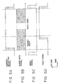
- Figs.5A through 5D show the sequence of control signals needed to embody the present invention.
- a burst data signal shown in Fig.5B comprises a header area with such a mark-to-space ratio of 1/2 as an alternate number of "1" and "0" at the head, and a data area following the header area.
- a reset signal shown in Fig.5C is issued for several bits after the detection of the first burst data is completed until the next burst data are inputted.
- a carrier detection signal shown in Fig.5A is issued when the burst data are inputted, and is canceled when the detection of the data is completed or the reset signal is inputted.
- a hold signal shown in Fig.5D is issued before the detection of the header area of the burst data is completed, and is canceled when the detection of the data is completed or the reset signal is inputted.
- the switch 12 In an initial state the switch 12 is connected to the initial potential generator circuit 11, and is switched to the digital level signal output from the digital signal amplitude regenerator circuit 10 by a carrier detection signal 17.
- the output from the switch 12 is branched into two after passing through the low-pass filter 13; one branched signal is connected to the signal input terminal of the limiting amplifier 15, and the other branched signal is connected to the pulse width compensation threshold generator circuit 14.
- the pulse width compensation threshold generator circuit 14 starts the threshold detection for compensating for the degradation in pulse width by the issuance of reset signal 18 along with the switching of the switch 12, terminates the threshold detection using a hold signal, holds the threshold, and provides the threshold to the reference potential terminal of the limiting amplifier 15.
- a reset signal 18 is issued, the carrier detection signal 17 is cancelled, the switch 12 is again connected to the initial potential generator circuit 11, and the output potential of the pulse width compensation threshold generator circuit 14 returns to the initial potential by the reset signal.
- the hold signal can also be generated in the burst pulse width compensation circuit 9. In the description below the reset signal is still assumed to be provided by the transmission system of the burst data.
- Fig.6 shows the first embodiment of the present invention.
- a pulse width compensation threshold generator circuit 50 includes a peak detector circuit 55 and a trough detector circuit 56, in which amplitude detection volume per unit time is restricted, and a voltage divider circuit 57.
- the peak and trough detector circuits 55 and 56 enter a voltage-follower state, and return to the initial potential during the time period in which the reset signal is input.
- a digital signal amplitude regenerator circuit 51 amplifies inputted digital signals, and the output is inputted to a switch 53.
- a carrier detection signal generator circuit 59 is connected to the input side of the digital signal amplitude regenerator circuit 51, and detects the carrier of the burst data.
- the output terminal of the switch 53 at first, is connected to an initial potential generator circuit 52 for providing a certain voltage, and is switched by a carrier detection signal 60 generated by the carrier detection signal generator circuit 59 to transfer a signal from the digital signal amplitude regenerator circuit 51 to a low-pass filter 54.
- the digital signal is smoothed by passing through the low-pass filter 54 and is inputted to a limiting amplifier 58, and is simultaneously inputted to the peak detector circuit 55 and the trough detector circuit 56.
- the peak detector circuit 55 and the trough detector circuit 56 reset a voltage value stored in the peak and the trough detector circuit 55 and 56, and start a new voltage detection.
- the peak detector circuit 55 detects the peak potential of a pulse of the burst data signal
- the trough detector circuit 56 detects the trough potential of a pulse of the burst data signal.
- such a high-speed detection so as to completely catch the potential with one bit is not performed.
- the detection speed is adjusted so that, for example, when the pulse width of the burst data signal is wide, the result of dividing the voltage detected by the peak detector circuit 55 and the voltage detected by the trough detector circuit 56 using the voltage divider circuit 57 may become close to the peak potential of the burst data signal.
- the detection speed is adjusted so the result of dividing the detected voltages by the voltage divider circuit 57 may become close to the trough potential of the burst data signal.
- the peak detector circuit 55 and the trough detector circuit 56 hold the potential close to the peak potential and the potential close to the trough potential of the burst data signal respectively.
- the output of the voltage divider circuit 57 is inputted to the limiting amplifier 58 as a threshold potential for pulse width compensation, whereby the degradation in pulse width is compensated for.
- Figs.7A and 7B show the peak and trough detections, threshold change and operations of the first embodiment.
- each detection since in the peak and trough detections where a detected volume per one bit is restricted, each detection operates according to the pulse width, and the threshold continues to come near to a wider pulse width until either the peak detection or the trough detection completely catches the digital signal level. Therefore, a pulse width compensation effect is obtained by terminating the detection before either the peak detection or the bottom detection reaches the digital signal level.
- the change volume per signal cycle of the peak detection value becomes bigger than the change volume per signal cycle of the trough detection value by the difference of the widths of the "1" level and the "0" level, and the threshold of the peak detection value becomes higher because of the lowering of the threshold of the trough detection value.
- Figs.7A and 7B show the case where the input pulse width to a pulse width compensation circuit 50 is wider than the original pulse width, and when starting the peak detection and trough detection from the digital DC level outputted by an initial potential generator circuit 52, the peak detection circuit 55 detects the "1" level of a waveform outputted from the low-pass filter 54 faster than detection of "0" level by the trough detection circle 56. Meanwhile, the trough detection circuit 56 does not detect the "0" level of the waveform outputted from the low-pass filter 54. Therefore, a value close to the "1" level can be obtained for the mean value of a threshold provided by the voltage divider 57.
- Fig. 7B shows the result of a limiting amplifier 58 compensating for the degradation in pulse width based on the threshold obtained in the process shown in Fig.7A.
- Fig.8 explains the role of a hold signal.
- the peak detection circuit 55 detects the peak potential of a pulse faster than the trough detection circuit 56.
- both the peak detection level and the trough detection level are stored by a hold signal.
- a process for narrowing the pulse width of a burst signal with an extended pulse width can be performed by holding the threshold close to the "1" level.
- the bottom detection circuit 56 tries to detect the "0" level of the output from the low-pass filter, and the detection level gradually falls.
- the peak detection circuit 55 since the peak detection circuit 55 has already detected the "1" level, the peak detection level is fixed to this level. Accordingly, when there is no holding, the level of the threshold being a mean value between the peak detection level and the trough detection level gradually falls, and behaves as shown by a non-holding threshold level in the diagram. If the degradation in pulse width is tried to be compensated for using this threshold with a diminished level, the width of the pulse can only be narrowed to a lesser degree.
- the trough detection circuit 56 detects the "0" level first, and then the peak detection circuit 55 gradually tries to detect the "1" level. At this time, the threshold level must be low in order to extend the pulse width. If there is no holding, the threshold level rises as the peak detection level gradually rises, and thereby an extension of the pulse width becomes unavailable.
- this embodiment is configured so that the degradation in pulse width may be compensated for by decreasing the speed of the peak detection and trough detection and holding the peak detection level and trough detection level by a hold signal after an appropriate detection time.
- Fig.9 shows the second embodiment of the present invention.
- a switch SW1 is turned off only while there is a hold signal, and switches SW2 and SW3 are turned on only while there is a reset signal.
- a resistor "r" has a value sufficient to reset the capacitor 84 sufficiently fast.
- a charge corresponding to the pulse width is discharged or charged in a capacitor 84 by the operation of a charge pump 80, a threshold voltage reflecting the pulse width is generated across the capacitor 84, the capacitor 84 is separated from the charge pump 80 by the switch SW1 while the detection is performed for a mark-to-space ratio of 1/2, and the pulse width is compensated for by storing the threshold.
- the switch 53 switches the output of a digital signal amplitude regenerator circuit 51 to the output of an initial potential generator circuit 52 based on a carrier detection signal 60 generated by a carrier detection signal generator circuit 59, and vice versa.
- the output of the initial potential generator circuit 52 is applied to the capacitor 84 through the switches SW2 and SW3, and is also applied to a limiting amplifier 58 as an initial value of the threshold while there is a reset signal.
- the switch SW1 is on, the switch SW1 being on hardly affects the threshold since the voltage supplied from the charge pump 80 corresponds to noise.
- the reset signal is canceled, the switches SW2 and SW3 are turned off, and the capacitor 84 receives voltage only through the charge pump 80.
- the capacitor 84 is supplied with voltage by burst data through the charge pump 80, since the carrier of burst data is almost simultaneously inputted.
- the charge pump 80 comprises different types of transistors 80-1 and 80-2.
- the charge pump 80 is configured so that when a signal from the low-pass filter 54 has a high potential, the transistor 80-1 is turned on, and when a signal from the low-pass filter 54 has a low potential, the transistor 80-2 is turned on.
- the transistors 80-1 and 80-2 are configured so that current discharged from the capacitor 84 and current charged to the capacitor 84 become equal if the mean voltage is equal to an initial potential. Accordingly, when the pulse width of the burst data is wide, the on- time of the transistor 80-1 becomes long, a high charge is stored in the capacitor 84, and the potential as a threshold to be applied to the limiting amplifier 58 becomes high. Conversely, when the pulse width of the burst data is narrow, the on-time of the transistor 80-2 becomes long, a high charge is removed from the capacitor 84, and the potential as a threshold to be applied to the limiting amplifier 58 becomes low.
- the potential obtained in this manner and generated by the charge stored in the capacitor 84 as a threshold is stored by turning off the switch SW1 according to the input of the hold signal 62, and the degradation in pulse width is compensated for while the data area of the burst data is inputted.
- Fig. 10 shows the third embodiment of the present invention.
- a switch SW1 is turned off only while there is a hold signal 62, and switches SW2 and SW3 are turned on only while there is a reset signal 61.
- a resistor "r" has a value sufficient to reset the capacitor 84 sufficiently fast.
- a threshold corresponding to the pulse width can be obtained by a mean value detection, the mean value detection is terminated while the detection is performed for a mark-to-space ratio of 1/2, and the degradation in pulse width is compensated for by storing the threshold.
- the burst data signal of which the amplitude is restored by a digital signal amplitude regenerator circuit 51 is inputted to a low-pass filter 54 through a switch 53, and the waveform is smoothed.
- the switch 53 is switched over so that the voltage of an initial potential generator circuit 52 may be applied to a limiting amplifier 58 and the SW1 side through the low-pass filter 54, since a carrier detection signal 60 is not outputted from a carrier detection signal generator circuit 59.
- a reset signal 61 is issued, the switches SW2 and SW3 close, the output voltage of the initial potential generator circuit 52 is applied to a capacitor 84, and the limiting amplifier 58 is provided with the initial potential for the threshold detection.
- the switches SW2 and SW3 open, and a signal from the low-pass filter 54 is applied to the capacitor 84.
- the voltage of the initial potential generator circuit 52 is applied to the capacitor 84 through the switch 53, the low-pass filter 54, the switch SW1 and a resistor 91.
- the burst data signal outputted from the digital signal amplitude regenerator circuit 51 and obtained through the low-pass filter 54 of which the waveform is smoothed is applied to the capacitor 84 through the switch SW1 and the resistor 91.
- a voltage corresponding to the pulse width of the inputted burst data signal is generated across the capacitor 84 by the operation of the resistor 91 and the capacitor 84.
- the switch SW1 is opened by a hold signal 62, the potential across the capacitor 84 is stored, and the potential is inputted to the reference terminal of the limiting amplifier 58.
- the limiting amplifier 58 restores the original waveform width of a burst data signal in which the waveform is degraded with the potential inputted from the reference terminal as the threshold and outputs the restored burst data signal.
- Fig. 11 shows the fourth embodiment of the present invention.
- the pulse width compensation circuit 100 of this embodiment compares the output of the peak detection circuit 55 and the output of the trough detection circuit 56 with the reference amplitude set by voltage comparators 102 and 103, respectively, the pulse width compensation circuit 100 issues a hold signal for terminating the detection when either of the outputs becomes greater or smaller than the reference amplitude, and the pulse width is compensated for without receiving an external hold signal by canceling a carrier detection signal or canceling the hold signal using a reset signal 61.
- the output of the peak detection circuit 55 and the output of the trough detection circuit 56 are inputted to the voltage comparators 102 and 103, respectively.
- a reference voltage is inputted to each of the voltage comparators, and whether or not the peak detection level detected by the peak detection circuit 55 is higher than a predetermined level is detected using the voltage comparator 102. Whether or not the trough detection level detected by the bottom detection circuit 56 is lower than a predetermined level is detected using the voltage comparator 103.
- the system is configured so that the detected results of the voltage comparators 102 and 103 may be inputted to a hold signal generator circuit 101, and when either the output of the peak detection circuit 55 or the output of the trough detection circuit 56 becomes greater or smaller than the predetermined level against the reference voltage, a hold signal may be outputted.
- the output of the hold signal is stopped by canceling the reset signal 61 received from a transmission system of burst data signals. For this reason, the reset signal 61 is inputted to the hold signal generator circuit 101.
- a carrier detection signal 60 can also be inputted to the hold signal generator circuit 101. In this case, it is considered that the cancellation of the hold signal is synchronized with the cancellation of the carrier detection signal 60.
- Fig.12 shows the fifth embodiment of the present invention.
- the pulse width compensation circuit 110 of this embodiment produces a difference amplitude from the output of a peak detection circuit 55 and the output of a trough detection circuit 56 using an amplitude subtraction circuit 111, the pulse width compensation circuit 110 compares the difference amplitude with a reference amplitude (approximately half of the digital level amplitude) set by a voltage comparator 112, the compensation circuit 110 issues a hold signal for terminating the detection by a hold signal generator circuit 113 when the difference amplitude becomes greater than the reference amplitude, and the pulse width is compensated for without receiving a hold signal from outside by canceling a carrier detection signal or canceling the hold signal using a reset signal 61.
- a reference amplitude approximately half of the digital level amplitude
- a burst data signal from a digital signal amplitude regenerator circuit 51 performs a peak detection and a trough detection of a waveform smoothed by a low-pass filter 54 using the peak detection circuit 55 and the trough detection circuit 56, respectively, the respective output is inputted to an amplitude subtraction circuit 111.
- the amplitude subtraction circuit 111 the difference in level of a peak detection level and a trough detection level is measured, and the result is transferred to the voltage comparator 112.
- the voltage comparator 112 is configured so as to input a voltage of approximately half of the difference in level between the "1" level and the "0" level of a burst data signal as a reference voltage, and compares the level from the amplitude subtraction circuit 111 and the reference voltage to determine whether or not it is greater than the reference voltage.
- the hold signal generator circuit 113 receives the detection result from the voltage comparator 112, and outputs a hold signal when the difference in level obtained by the amplitude subtraction circuit 111 becomes greater than the above-mentioned predetermined voltage value. This is, in order to hold a threshold obtained by a voltage divider circuit 57, an appropriate peak detection level and an appropriate trough detection level are obtained when a peak detection and a trough detection are started from an initial value provided by an initial potential generator circuit 52, and after a certain continuation of the detection, a certain difference in level is generated between the peak detection level and the trough detection level.
- a hold signal can be canceled when a reset signal 61 is inputted to the hold signal generator circuit 113 or when a carrier detection signal 60 is inputted to the hold signal generator circuit 113.
- Fig. 13 shows the sixth embodiment of the present invention.
- the pulse width compensation circuit 120 of this embodiment compensates for the degradation in pulse width without receiving an external hold signal by obtaining a hold signal 122 for terminating the detection by the issuance of a carrier detection signal 17, using a delay circuit 121, and the cancellation of a carrier detection signal 17 or a reset signal 18.
- a pulse width threshold generator circuit 14 can have any of the configurations shown in Figs.6, 9 and 10.
- a hold signal is obtained by providing the carrier detection signal with an appropriate delay using the delay circuit 121.
- a threshold is generated in this header area.
- the threshold is generated using the peak detection level and trough detection level as described earlier, it is necessary to appropriately estimate a delay time provided to the hold signal 122 by the delay circuit 121, since the speeds of the peak detection and trough detection are not set too fast.
- This delay time shall be set at the design stage of a burst pulse width compensation circuit 120, taking into consideration the number of bits and transmission speed of the header area, time needed to generate the threshold, etc.
- the hold signal can be canceled when a reset signal 18 is inputted to a pulse width compensation threshold generator circuit 14, or a carrier detection signal 17 can be directly inputted to the pulse width compensation threshold generator circuit 14, although not shown in the diagram.
- Fig. 14 shows the seventh embodiment of the present invention.
- the degradation in pulse width is compensated for without receiving a hold signal by generating a hold signal for terminating the detection using a hold signal generator circuit 131, when the digital signal output is counted by a counter circuit 132, from when a carrier detection signal is issued and the count exceeds a set number of counts, and canceling the carrier detection signal 17 or canceling the hold signal using a reset signal 18.
- This embodiment comprises a counter circuit 132 for counting the number of bits of the smoothed burst data signal, which are outputted from a low-pass filter 13 and a hold signal generator circuit 131 for generating a hold signal.
- a reset signal is inputted from a transmission system of the burst data
- the reset signal is transferred to a carrier detection signal generator circuit 16, the counter circuit 132, the hold signal generator circuit 131 and a pulse width compensation threshold generator circuit 14 to reset these circuits to receive the next burst data.
- the detection signal generator circuit 16 When a burst data signal is inputted, the detection signal generator circuit 16 generates a carrier detection signal 17, and the burst data signal is transferred to the low-pass filter 13 from the digital signal amplitude regenerator circuit 10 through the switch 12.
- the burst data signal outputted from the low-pass filter 13 in which the waveform is smoothed is transferred to the counter circuit 132, and the number of bits of the header area is counted in order.
- the number counted by the counter circuit 132 is inputted to the hold signal generator circuit 131.
- the hold signal generator circuit 131 a predetermined count number is stored, and when the number counted by the counter circuit 132 exceeds this predetermined count number, the hold signal generator circuit 131 generates a hold signal, and inputs the hold signal to the pulse width compensation generator circuit 14.
- the pulse width compensation generator circuit 14 stores the threshold, and compensates the degradation in pulse width of the data area following the header area as described above.
- the hold signal can be canceled when the reset signal is inputted or the system can be configured so that the carrier detection signal 17 may be inputted to the hold signal generator circuit 131 and the hold signal may be canceled when the carrier detection signal 17 is canceled.
- the count number set in the hold signal generator circuit 131 estimates the number of bits of a header area needed for the pulse width compensation threshold generator circuit 14 to generate an appropriate threshold, and should be appropriately determined when the pulse width compensation circuit 130 is designed. In this case, the time needed for the pulse width compensation threshold generator circuit 14 to acquire an appropriate threshold, the number of bits of a header area, transmission speed, etc. shall be taken into consideration.
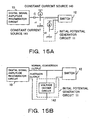
- Figs.15A and 15B show an embodiment of an initial potential generator circuit.
- an initial potential generator circuit 11 resistant to power voltage fluctuations can be obtained by providing a digital signal with a DC level at the output end of a digital signal amplitude regenerator circuit 10.
- the DC component is removed by providing the output end of the digital signal amplitude regenerator circuit 10 with a capacitor C. Then, a new DC component is provided using a constant-current source 140 and a resistor r1.
- a new DC component is provided using a constant-current source 140 and a resistor r1.
- the level of the DC voltage component of the burst data becomes equal to the initial level provided by the initial potential generator circuit 11 when the current of the constant voltage source 140 is generated from the same power voltage, even if an initial potential provided by the initial potential generator circuit 11 changes due to a fluctuation in the power voltage, etc., and thereby the setting process of the threshold can be started from an optimal initial value.
- an initial potential generator circuit 11 resistant to power voltage fluctuations can be obtained by causing the output of the initial potential generator circuit 11 to fluctuate in the same direction as a digital signal output, when the power voltage fluctuates.
- the system is configured so that when a burst data signal received by the digital amplitude regenerator circuit 10 is amplified and reproduced, a normal conversion output and an inversion output obtained by inverting this normal conversion output between the "1" level and "0" level of the digital output level may be generated, and both the outputs may be inputted to a voltage divider circuit 142 of the initial potential generator circuit 11.
- the voltage divider 142 divides the voltage values of the normal conversion output and inversion output, and provides an initial potential. According to this embodiment, since the initial potential is provided based on a transmitted burst data signal and the initial potential fluctuates in the same manner when the DC voltage value of the burst data signal fluctuates, the setting process of a threshold can also be executed from an optimal initial level.
- the initial potential for a threshold setting process cannot be biased to a "1" level or "0" level, since the normal conversion output potential and the inversion output potential are divided are provided as an initial potential.
- pulse width degradation of a burst data signal can be compensated for after being amplified up to an original digital level.
Landscapes
- Engineering & Computer Science (AREA)
- Physics & Mathematics (AREA)
- Nonlinear Science (AREA)
- Power Engineering (AREA)
- Computer Networks & Wireless Communication (AREA)
- Signal Processing (AREA)
- Dc Digital Transmission (AREA)
- Optical Communication System (AREA)
- Manipulation Of Pulses (AREA)
Claims (22)
- Circuit pour compenser la dégradation de la largeur d'impulsion des données en rafale, comportant:un moyen de génération de seuil (14) adapté pour détecter un seuil pour compenser la dégradation de la largeur d'impulsion à partir d'un signal de données en rafale transmis ;un moyen de compensation de largeur d'impulsion (9, 50) adapté pour reformer la largeur d'impulsion en fonction du seuil généré par le moyen de génération de seuil; etun moyen de génération de potentiel initial (11, 52) adapté pour délivrer un potentiel initial au moyen de génération de seuil lorsque le moyen de génération de seuil détecte le seuil.
- Circuit pour compenser la dégradation de la largeur d'impulsion de données en rafale selon la revendication 1, dans lequel
ledit moyen de génération de seuil (14) étant adapté pour délivrer un seuil en poursuivant et en détectant la valeur de crête et la valeur de creux du niveau de signal du signal de données en rafale, et en divisant la valeur de crête et la valeur minimale obtenue. - Circuit pour compenser la dégradation de la largeur d'impulsion de données en rafale selon la revendication 2, dans lequel
ledit moyen de génération de seuil (14) étant adapté pour maintenir la valeur de crête et la valeur minimale avant que soit la détection de crête soit la détection de creux détecte la valeur de crête ou la valeur de creux réelle lorsque la largeur d'impulsion du signal de données en rafale n'est pas appropriée. - Circuit pour compenser la dégradation de la largeur d'impulsion de données en rafale selon la revendication 3, dans lequel
ledit seuil étant adapté pour une mémorisation lorsque ladite valeur de détection de crête ou ladite valeur de détection de creux dépasse ou tombe au-dessous de niveaux prédéterminés. - Circuit pour compenser la dégradation de la largeur d'impulsion de données en rafale selon la revendication 3, dans lequel
ledit seuil étant adapté pour une mémorisation lorsque la différence de niveau entre ladite valeur de détection de crête et ladite valeur de détection de creux dépasse ou tombe au-dessous de valeurs prédéterminées. - Circuit pour compenser la dégradation de la largeur d'impulsion de données en rafale selon la revendication 1, dans lequel
en générant un potentiel correspondant à la largeur d'impulsion d'un signal de données en rafale à chaque extrémité du condensateur en appliquant une tension correspondant à la valeur de tension du signal de données en rafale reçu au condensateur, ledit moyen de génération de seuil (14) utilise ce potentiel en tant que seuil. - Circuit pour compenser la dégradation de la largeur d'impulsion de données en rafale selon la revendication 1, dans lequel
ledit moyen de génération de seuil (14) étant adapté pour achever la détection de seuil à un moment prédéterminé après la détection des données en rafale, et mémoriser le seuil. - Circuit pour compenser la dégradation de la largeur d'impulsion de données en rafale selon la revendication 1, dans lequel
ledit moyen de génération de seuil (14) étant adapté pour achever la détection de seuil après qu'un nombre prédéterminé de bits à partir du bit des données en rafale a été détecté, et mémoriser le seuil. - Circuit pour compenser la dégradation de la largeur d'impulsion de données en rafale selon la revendication 1, dans lequel
ledit circuit de compensation de largeur d'impulsion (9, 50) comprend un moyen pour délivrer le signal de données en rafale dont le potentiel à courant continu est supprimé par un nouveau potentiel à courant continu après qu'un potentiel à courant continu soit supprimé dudit signal de données en rafale reçu, et
ledit moyen de génération de potentiel initial (11, 52) délivre le même potentiel à courant continu que le nouveau potentiel à courant continu délivré aux données en rafale en tant que potentiel initial. - Circuit pour compenser la dégradation de la largeur d'impulsion de données en rafale selon la revendication 1, dans lequel
ledit moyen de génération de potentiel initial (11, 52) délivre le potentiel obtenu en divisant potentiellement le signal de conversion normal et le signal d'inversion du signal de données en rafale en tant que potentiel initial. - Circuit pour compenser la dégradation de la largeur d'impulsion de données en rafale selon la revendication 1, caractérisé en ce qu'il possède une zone d'en-tête avec un rapport cyclique prédéterminé et une zone de données pour mémoriser des données, dans lequelle moyen de compensation de largeur d'impulsion (9, 50) comporte en outreun moyen de commutation (12, 53) pour commuter le potentiel initial au signal de données en rafale lorsque le signal de données en rafale est entré ;un filtre passe bas (13, 54) possédant une fréquence de coupure similaire par rapport à une vitesse de transmission de signal pour lisser la forme d'onde d'une sortie provenant du moyen de commutation;un amplificateur de limitation (15, 58) pour amplifier la sortie dudit filtre passe bas et le délivrer à une borne d'entrée de signal ; etle moyen de génération de seuil (14) est adapté pour commencer une détection de seuil pour compenser la dégradation de la largeur d'impulsion en commutant le commutateur lorsque le signal de données en rafale est entré, terminer la détection de seuil avant que la détection de la zone d'en-tête des données en rafale soit achevée, et mémoriser le seuil jusqu'à ce que le signal de données en rafale soit achevé, dans lequella sortie du moyen de génération de seuil est reliée à la borne de potentiel de référence dudit amplificateur de limitation, et la dégradation de la largeur d'impulsion du signal de données en rafale est compensée par le potentiel délivré à la borne de potentiel de référence en tant que seuil.
- Circuit pour compenser la dégradation de la largeur d'impulsion de données en rafale selon la revendication 11, dans lequel ledit moyen de génération de seuil comporte en outre
un moyen de détection de crête (55) pour détecter le niveau de crête du signal de données en rafale en limitant le volume détecté par unité de temps ;
un moyen de détection de creux (56) pour détecter le niveau de creux du signal de données en rafale en limitant le volume détecté par unité de temps ; et
un moyen diviseur de tension (57) pour générer un seuil à partir d'un potentiel de détection de crête et d'un potentiel de détection de creux, et
les moyens de détection de crête et de creux mémorisant le seuil tant que la détection de ladite zone de données continue. - Circuit pour compenser la dégradation de la largeur d'impulsion de données en rafale selon la revendication 11, dans lequel
le seuil est détecté par une pompe de charge (80) conçue de sorte qu'un courant de charge et un courant de charge peuvent délivrer le volume équivalent de courant lorsqu'une valeur moyenne du signal de données en rafale est équivalente à un potentiel initial. - Circuit pour compenser la dégradation de la largeur d'impulsion de données en rafale selon la revendication 11, dans lequel
le seuil est détecté en détectant une valeur moyenne en utilisant une résistance et une capacité. - Circuit pour compenser la dégradation de la largeur d'impulsion de données en rafale selon la revendication 11, dans lequel
un signal de maintien (19, 62, 122) pour ordonner la mémorisation dudit seuil détecté dans ledit moyen de génération de seuil (14) est généré dans le circuit de compensation de largeur d'impulsion en utilisant chacun ou les deux d'un signal de détection de porteuse pour indiquer qu'un signal de données en rafale est détecté, et d'un signal de réinitialisation généré afin d'ordonner la restauration du seuil lorsqu'il n'y a pas de signal de données en rafale. - Circuit pour compenser la dégradation de la largeur d'impulsion de données en rafale selon la revendication 12, comportant en outre
un moyen de comparaison de tension (102, 103) pour comparer les sorties des moyens de détection de crête et de creux (55, 56), avec le potentiel de référence déterminé respectif,
dans lequel en délivrant un signal de maintien pour ordonner la mémorisation dudit seuil détecté dans ledit moyen de génération de seuil (14) lorsque chacune des sorties dépasse une amplitude de référence, et en annulant le signal de maintien en annulant un signal de détection de porteuse pour indiquer que le signal de données en rafale est détecté ou en utilisant un signal de réinitialisation généré afin d'ordonner la réinitialisation du seuil lorsqu'il n'y a pas de signal en rafale, la fonction du signal de maintien est effectuée. - Circuit pour compenser la dégradation de la largeur d'impulsion de données en rafale selon la revendication 12, comportant en outre
un moyen de comparaison de tension (112) pour comparer la différence de la sortie des moyens de détection de crête et de creux à un potentiel de référence déterminée,
dans lequel en délivrant un signal de maintien pour ordonner la mémorisation dudit seuil détecté dans ledit moyen de génération de seuil (55, 56, 57) lorsque la différence de sortie dépasse une amplitude de référence, et en annulant le signal de maintien en annulant un signal de détection de porteuse pour indiquer qu'un signal de données en rafale est détecté ou en utilisant un signal de réinitialisation généré afin d'ordonner la réinitialisation du seuil lorsqu'il n'existe pas de signal en rafale, la fonction du signal de maintien est effectuée. - Circuit pour compenser la dégradation de la largeur d'impulsion de données en rafale selon la revendication 11, comportant en outre
un moyen de retard (121) pour retarder un signal de détection de porteuse indiquant que le signal de données en rafale est détecté à un temps prédéterminé,
dans lequel en délivrant un signal de maintien pour ordonner la mémorisation dudit seuil détecté dans ledit moyen de génération de seuil (14) retardant la délivrance du signal porteur pendant le temps prédéterminé par le moyen de retard (121), et en annulant le signal de maintien en annulant le signal de détection de porteuse indiquant que le signal de données en rafale est détecté ou en utilisant un signal de réinitialisation généré afin d'ordonner la réinitialisation du seuil lorsqu'il n'existe pas de signal en rafale, la fonction du signal de maintien est exécutée. - Circuit pour compenser la dégradation de la largeur d'impulsion de données en rafale selon la revendication 11, comportant en outre
un moyen de comptage (132) pour compter la sortie du signal numérique du signal de données en rafale conformément à la délivrance d'un signal de détection de porteuse indiquant que le signal de données en rafale est détecté,
dans lequel en délivrant un signal de maintien pour ordonner la mémorisation dudit seuil détecté dans ledit moyen de génération de seuil (14) après un nombre prédéterminé de bits, et en annulant le signal de maintien en annulant un signal de détection de porteuse indiquant que le signal de données en rafale est détecté ou en utilisant un signal de réinitialisation généré afin d'ordonner la réinitialisation du seuil lorsqu'il n'existe pas de signal en rafale, la fonction du signal de maintien est exécutée. - Circuit pour compenser la dégradation de la largeur d'impulsion de données en rafale selon la revendication 11, comportant en outre
un premier moyen de serrage (11) pour délivrer le signal numérique avec un niveau CC,
dans lequel un moyen de génération de potentiel initial (11, 52) résistant aux fluctuations de tension d'alimentation peut être réalisé en coupant la composante de courant continu du signal numérique en reliant un condensateur à la sortie de niveau numérique du signal de données en rafale en série, en délivrant un nouveau niveau CC au signal numérique par ledit moyen de serrage, et en constituant ledit moyen de génération de potentiel initial (11, 52) en utilisant un second moyen de serrage comportant les mêmes caractéristiques que le premier moyen de serrage. - Circuit pour compenser la dégradation de la largeur d'impulsion de données en rafale selon la revendication 11, dans lequel
un moyen de génération de potentiel initial (11, 52) résistant aux fluctuations de tension d'alimentation peut être réalisé en reliant la sortie de conversion normale et la sortie d'inversion du signal de niveau numérique du signal de données en rafale à un moyen diviseur de tension (57), et en utilisant la sortie du moyen diviseur de tension (57) en tant que sortie du moyen de génération de valeur initiale (14). - Procédé pour compenser la dégradation de la largeur d'impulsion de données en rafale possédant une zone d'en-tête avec un rapport cyclique de 1/2 et une zones de données pour mémoriser les données, comportant les étapes consistant à :délivrer un potentiel initial lors de la détection d'un seuil pour compenser la dégradation de la largeur d'impulsion ;commuter le potentiel initial à un signal de données en rafale lorsque le signal de données en rafale est entré ;supprimer les composantes à haute fréquence afin de lisser la forme d'onde du signal de données en rafale ;commencer une détection de seuil pour compenser la dégradation de la largeur d'impulsion lorsque le signal de données en rafale est entré, terminer la détection de seuil avant que la détection de la zone d'en-tête des données en rafale soit achevée, et mémoriser le seuil jusqu'à ce que la détection du signal de données en rafale soit achevée; etreformer la largeur d'impulsion du signal de données en rafale dont la forme d'onde est lissée, en fonction du seuil.
Applications Claiming Priority (2)
| Application Number | Priority Date | Filing Date | Title |
|---|---|---|---|
| JP3436998 | 1998-02-17 | ||
| JP10034369A JPH11234349A (ja) | 1998-02-17 | 1998-02-17 | バーストパルス幅補償回路及びパルス幅補償方法 |
Publications (3)
| Publication Number | Publication Date |
|---|---|
| EP0936737A2 EP0936737A2 (fr) | 1999-08-18 |
| EP0936737A3 EP0936737A3 (fr) | 2000-01-05 |
| EP0936737B1 true EP0936737B1 (fr) | 2007-04-18 |
Family
ID=12412266
Family Applications (1)
| Application Number | Title | Priority Date | Filing Date |
|---|---|---|---|
| EP98111198A Expired - Lifetime EP0936737B1 (fr) | 1998-02-17 | 1998-06-18 | Circuit et procédé pour compenser la dégradation de la largeur d' impulsion de données en rafale |
Country Status (4)
| Country | Link |
|---|---|
| US (1) | US6393069B1 (fr) |
| EP (1) | EP0936737B1 (fr) |
| JP (1) | JPH11234349A (fr) |
| DE (1) | DE69837593T2 (fr) |
Families Citing this family (13)
| Publication number | Priority date | Publication date | Assignee | Title |
|---|---|---|---|---|
| FR2806855B1 (fr) * | 2000-03-21 | 2002-06-21 | St Microelectronics Sa | Demodulateur d'un signal alternatif module en amplitude |
| DE10122023A1 (de) * | 2001-05-07 | 2002-11-21 | Infineon Technologies Ag | Anordnung und Verfahren zur Ermittlung des jeweils aktuellen Pegels eines digitalen Signals |
| US6714598B2 (en) * | 2002-04-29 | 2004-03-30 | Scientific-Atlanta, Inc. | Burst-mode combining of reverse path radio frequency signals |
| US7663697B2 (en) * | 2005-12-08 | 2010-02-16 | Seiko Epson Corporation | Sync-threshold adjust |
| JP4905087B2 (ja) | 2006-11-30 | 2012-03-28 | 富士通オプティカルコンポーネンツ株式会社 | 受信装置 |
| JP5176505B2 (ja) * | 2007-12-03 | 2013-04-03 | 富士通オプティカルコンポーネンツ株式会社 | 光受信装置,光局側装置および光ネットワークシステム |
| US8131238B2 (en) * | 2008-03-20 | 2012-03-06 | Infineon Technologies Ag | Carrier signal detection |
| TWI454042B (zh) * | 2011-05-04 | 2014-09-21 | Actron Technology Corp | 相位偵測裝置及其方法 |
| TWI449322B (zh) * | 2011-06-03 | 2014-08-11 | Actron Technology Corp | 交流發電機之相位偵測裝置及其方法 |
| CN102841253A (zh) * | 2011-06-21 | 2012-12-26 | 朋程科技股份有限公司 | 交流发电机的相位检测装置及其方法 |
| JP2012090284A (ja) * | 2011-11-14 | 2012-05-10 | Fujitsu Optical Components Ltd | 光受信装置,光局側装置および光ネットワークシステム |
| KR102544166B1 (ko) * | 2018-04-19 | 2023-06-16 | 에스케이하이닉스 주식회사 | 펄스 폭 보상 회로 및 이를 이용하는 반도체 장치 |
| CN113452934B (zh) * | 2020-03-26 | 2024-02-13 | 瑞昱半导体股份有限公司 | 图像播放系统及其具有同步数据传输机制的图像数据传输装置及方法 |
Family Cites Families (11)
| Publication number | Priority date | Publication date | Assignee | Title |
|---|---|---|---|---|
| JPS577627A (en) * | 1980-06-17 | 1982-01-14 | Sony Corp | Waveform shaping circuit for code signal |
| GB2164812B (en) * | 1982-07-05 | 1986-12-10 | Matsushita Electric Industrial Co Ltd | Teletext decoder with slicing circuit |
| US5359238A (en) | 1992-08-04 | 1994-10-25 | Ford Motor Company | Analog to digital interface circuit with internal resistance compensation and integrity verification |
| US5281810A (en) | 1992-12-30 | 1994-01-25 | Allen-Bradley Company, Inc. | Photoelectric control unit adapted for determining its own operating margin having dual variable-gain amplifier |
| JP3115739B2 (ja) | 1993-01-27 | 2000-12-11 | シャープ株式会社 | パルス光受信回路 |
| US5373400A (en) | 1993-12-01 | 1994-12-13 | Analog Devices, Inc. | Dynamic threshold updating circuit for a maximum likelihood detector using both positive and negative comparators |
| KR100282936B1 (ko) * | 1994-12-24 | 2001-03-02 | 윤종용 | 디스크 구동장치에 있어서 신호처리를 위한 데이타 검출레벨 조정회로 |
| JP3301889B2 (ja) | 1995-06-15 | 2002-07-15 | 日本オプネクスト株式会社 | バースト光受信回路 |
| JPH09186562A (ja) | 1995-12-28 | 1997-07-15 | Matsushita Electric Ind Co Ltd | 増幅回路 |
| US6163580A (en) * | 1997-06-09 | 2000-12-19 | Sigmatel, Inc. | Method and apparatus for data detection with an enhanced adaptive threshold |
| JP3347053B2 (ja) | 1998-04-17 | 2002-11-20 | 日立建機株式会社 | オフセットブーム式建設機械のオフセット機構 |
-
1998
- 1998-02-17 JP JP10034369A patent/JPH11234349A/ja not_active Withdrawn
- 1998-06-16 US US09/098,229 patent/US6393069B1/en not_active Expired - Lifetime
- 1998-06-18 EP EP98111198A patent/EP0936737B1/fr not_active Expired - Lifetime
- 1998-06-18 DE DE69837593T patent/DE69837593T2/de not_active Expired - Lifetime
Also Published As
| Publication number | Publication date |
|---|---|
| US6393069B1 (en) | 2002-05-21 |
| EP0936737A2 (fr) | 1999-08-18 |
| JPH11234349A (ja) | 1999-08-27 |
| DE69837593T2 (de) | 2007-12-27 |
| EP0936737A3 (fr) | 2000-01-05 |
| DE69837593D1 (de) | 2007-05-31 |
Similar Documents
| Publication | Publication Date | Title |
|---|---|---|
| EP0936737B1 (fr) | Circuit et procédé pour compenser la dégradation de la largeur d' impulsion de données en rafale | |
| US5703506A (en) | Signal processing method | |
| JP4532563B2 (ja) | 光受信器およびその識別閾値生成方法 | |
| EP0197666B1 (fr) | Appareil optique de reproduction d'informations | |
| US4063183A (en) | Adaptive equalizer with improved distortion analysis | |
| JP4387078B2 (ja) | 光受信器 | |
| JP2962218B2 (ja) | ディジタル光受信回路 | |
| JP3435420B2 (ja) | 自動識別レベル制御回路 | |
| JP2000516378A (ja) | 自動利得制御回路 | |
| US6337887B1 (en) | Burst receiving circuit and control method thereof | |
| JP3489087B2 (ja) | 光バースト伝送における反射認識方法および装置 | |
| JP2003158497A (ja) | 信号断検出回路及びそれを用いた光受信装置 | |
| JP2825054B2 (ja) | 2線式時分割伝送方式の受信方法と受信回路 | |
| JP4099994B2 (ja) | 位相ロック・ループ回路 | |
| JP2772193B2 (ja) | 信号識別回路における直流再生方式 | |
| JP2933449B2 (ja) | 自動利得制御回路及びこれを用いたデータ記憶装置 | |
| JPH10124890A (ja) | トラッキング誤差信号検出装置 | |
| JP2748875B2 (ja) | クロック抽出回路 | |
| EP0782264A2 (fr) | Récepteur numérique à seuils adaptifs | |
| JPH11328858A (ja) | 高域強調フィルタのブ―スト調整方法 | |
| JP3821726B2 (ja) | 磁気テープ装置におけるpll同期検出回路および方法 | |
| JP3505605B2 (ja) | 自動利得制御回路 | |
| JPH03108832A (ja) | 再生中継器 | |
| EP0782263A1 (fr) | Détecteur de flancs avec hystéresis | |
| JPS6122487B2 (fr) |
Legal Events
| Date | Code | Title | Description |
|---|---|---|---|
| PUAI | Public reference made under article 153(3) epc to a published international application that has entered the european phase |
Free format text: ORIGINAL CODE: 0009012 |
|
| AK | Designated contracting states |
Kind code of ref document: A2 Designated state(s): DE FR GB |
|
| AX | Request for extension of the european patent |
Free format text: AL;LT;LV;MK;RO;SI |
|
| PUAL | Search report despatched |
Free format text: ORIGINAL CODE: 0009013 |
|
| AK | Designated contracting states |
Kind code of ref document: A3 Designated state(s): AT BE CH CY DE DK ES FI FR GB GR IE IT LI LU MC NL PT SE |
|
| AX | Request for extension of the european patent |
Free format text: AL;LT;LV;MK;RO;SI |
|
| 17P | Request for examination filed |
Effective date: 20000124 |
|
| AKX | Designation fees paid |
Free format text: DE FR GB |
|
| 17Q | First examination report despatched |
Effective date: 20050504 |
|
| GRAP | Despatch of communication of intention to grant a patent |
Free format text: ORIGINAL CODE: EPIDOSNIGR1 |
|
| GRAS | Grant fee paid |
Free format text: ORIGINAL CODE: EPIDOSNIGR3 |
|
| GRAA | (expected) grant |
Free format text: ORIGINAL CODE: 0009210 |
|
| AK | Designated contracting states |
Kind code of ref document: B1 Designated state(s): DE FR GB |
|
| REF | Corresponds to: |
Ref document number: 69837593 Country of ref document: DE Date of ref document: 20070531 Kind code of ref document: P |
|
| ET | Fr: translation filed | ||
| PLBE | No opposition filed within time limit |
Free format text: ORIGINAL CODE: 0009261 |
|
| STAA | Information on the status of an ep patent application or granted ep patent |
Free format text: STATUS: NO OPPOSITION FILED WITHIN TIME LIMIT |
|
| 26N | No opposition filed |
Effective date: 20080121 |
|
| PGFP | Annual fee paid to national office [announced via postgrant information from national office to epo] |
Ref country code: GB Payment date: 20140618 Year of fee payment: 17 |
|
| PGFP | Annual fee paid to national office [announced via postgrant information from national office to epo] |
Ref country code: DE Payment date: 20140611 Year of fee payment: 17 |
|
| PGFP | Annual fee paid to national office [announced via postgrant information from national office to epo] |
Ref country code: FR Payment date: 20140609 Year of fee payment: 17 |
|
| REG | Reference to a national code |
Ref country code: DE Ref legal event code: R119 Ref document number: 69837593 Country of ref document: DE |
|
| GBPC | Gb: european patent ceased through non-payment of renewal fee |
Effective date: 20150618 |
|
| REG | Reference to a national code |
Ref country code: FR Ref legal event code: ST Effective date: 20160229 |
|
| PG25 | Lapsed in a contracting state [announced via postgrant information from national office to epo] |
Ref country code: DE Free format text: LAPSE BECAUSE OF NON-PAYMENT OF DUE FEES Effective date: 20160101 Ref country code: GB Free format text: LAPSE BECAUSE OF NON-PAYMENT OF DUE FEES Effective date: 20150618 |
|
| PG25 | Lapsed in a contracting state [announced via postgrant information from national office to epo] |
Ref country code: FR Free format text: LAPSE BECAUSE OF NON-PAYMENT OF DUE FEES Effective date: 20150630 |