EP0937334B1 - Anordnung zum schutz der ausgangstransistoren in einem leistungsverstärker - Google Patents
Anordnung zum schutz der ausgangstransistoren in einem leistungsverstärker Download PDFInfo
- Publication number
- EP0937334B1 EP0937334B1 EP97912626A EP97912626A EP0937334B1 EP 0937334 B1 EP0937334 B1 EP 0937334B1 EP 97912626 A EP97912626 A EP 97912626A EP 97912626 A EP97912626 A EP 97912626A EP 0937334 B1 EP0937334 B1 EP 0937334B1
- Authority
- EP
- European Patent Office
- Prior art keywords
- power amplifier
- current
- temperature
- transistor
- output transistors
- Prior art date
- Legal status (The legal status is an assumption and is not a legal conclusion. Google has not performed a legal analysis and makes no representation as to the accuracy of the status listed.)
- Expired - Lifetime
Links
- 230000005540 biological transmission Effects 0.000 description 2
- XUIMIQQOPSSXEZ-UHFFFAOYSA-N Silicon Chemical compound [Si] XUIMIQQOPSSXEZ-UHFFFAOYSA-N 0.000 description 1
- 230000003321 amplification Effects 0.000 description 1
- 238000010586 diagram Methods 0.000 description 1
- 238000003199 nucleic acid amplification method Methods 0.000 description 1
- 229910052710 silicon Inorganic materials 0.000 description 1
- 239000010703 silicon Substances 0.000 description 1
Images
Classifications
-
- H—ELECTRICITY
- H03—ELECTRONIC CIRCUITRY
- H03F—AMPLIFIERS
- H03F1/00—Details of amplifiers with only discharge tubes, only semiconductor devices or only unspecified devices as amplifying elements
- H03F1/30—Modifications of amplifiers to reduce influence of variations of temperature or supply voltage or other physical parameters
-
- H—ELECTRICITY
- H03—ELECTRONIC CIRCUITRY
- H03F—AMPLIFIERS
- H03F1/00—Details of amplifiers with only discharge tubes, only semiconductor devices or only unspecified devices as amplifying elements
- H03F1/52—Circuit arrangements for protecting such amplifiers
-
- H—ELECTRICITY
- H03—ELECTRONIC CIRCUITRY
- H03F—AMPLIFIERS
- H03F2200/00—Indexing scheme relating to amplifiers
- H03F2200/468—Indexing scheme relating to amplifiers the temperature being sensed
Definitions
- the invention relates to an arrangement for protecting a power amplifier and, specifically, to an arrangement for protecting, in a power amplifier, the output transistors against temperatures exceeding a certain temperature.
- a temperature sensing transistor adjacent to the output transistors in the power amplifier to sense the temperature of the output transistors and influence the power amplifier when its temperature has reached a predetermined temperature value.
- temperature controllers normally operate in such a manner that at too high a silicon temperature, the power amplifier is turned off in order to let the output transistors cool to a lower temperature. When this lower temperature is reached, the power amplifier is again turned on and, anew, the temperature rises. If the cause of the too high temperature remains, the power amplifier will, thus, alternately be turned off and on.
- the power amplifier alternately is turned off and on constitutes a problem in case the power amplifier constitutes the output stage of e.g. a subscriber line interface circuit whose operation is monitored by means of a microprocessor or a computer. Moreover, the transmission of e.g. speech and/or date through the line interface circuit will be impossible when the operation of the output stage is disturbed in this manner.
- the object of the invention is to bring about an arrangement which eliminates the problems with today's temperature controllers.
- the transmission of speech and/or data through e.g. the above line interface circuit can, thus, continue undisturbed until the line current supplied by the power amplifier becomes so low that a device, e.g. a telephone set, connected to the line, ceases to function.
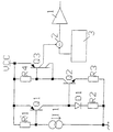
- the single figure shows a circuit diagram of an embodiment of an arrangement according to the invention for protecting output transistors (not shown) in a power amplifier 1 against temperatures exceeding a predetermined temperature value.
- the arrangement according to the invention comprises a temperature sensing transistor Q1 which in a manner not shown, is arranged adjacent to the output transistors (not shown) of the power amplifier 1 to sense their temperature.
- thermosensor not just a temperature sensing transistor has to be used to sense the temperature of the output transistors, but that any suitable temperature sensor, e.g. a diode, may be used.
- the temperature sensing transistor Q1 is adapted, in a manner to be described below, to vary the driving current of the power amplifier 1 inversely proportional to the temperature of the output transistors for temperatures between a first temperature value and a predetermined higher, second temperature value.
- the emitter of the temperature sensing transistor Q1 is connected to a supply voltage VCC, while its base is connected, on the one hand, to the supply voltage VCC via a resistor R1 and, on the other hand, to ground via a current generator I1.
- the collector of the transistor Q1 is connected to the interconnection point between the base of a transistor Q2 and the anode of a diode D1.
- the cathode of the diode D1 is connected to ground via a resistor R2.
- the emitter of the transistor Q2 is connected to ground via a resistor R3, while its collector is connected to the supply voltage VCC via a resistor R4.
- the interconnection point between the collector of the transistor Q2 and the resistor R4 is connected to the base as well as a first collector of a multi-collector transistor Q3 whose emitter is connected to the supply voltage VCC.
- a second collector of the transistor Q3 is connected to one input terminal of a current subtraction circuit 2 whose second input terminal is connected to the output terminal of a driving circuit 3 and whose output terminal is connected to the input terminal of the power amplifier 1.
- the driving circuit 3 is adapted to output on its output terminal, a current to the second input terminal of the subtraction circuit 2 for driving the power amplifier 1.
- the subtraction circuit 2 is adapted to subtract from the current received from the driving circuit 3, the current received from the second collector of the transistor Q3 and supply the resulting difference current as driving current to the input terminal of the power amplifier 1.
- the base-emitter path of the transistor Q1 is biased to a voltage corresponding to the temperature at which the transistor is to be turned on and the driving current to the power amplifier 1 is to be reduced.
- This voltage is set by the resistance of the resistor R1 and by the value of the current in the current generator I1.
- the current mirror formed by the diode D1 and the transistor Q2, constitutes together with the resistors R2 and R3 an amplifier for amplifying a collector current of the transistor Q1.
- a threshold value is set for the current from this amplifier, i.e. the collector current of the transistor Q2. For currents exceeding this threshold value, the multi-collector transistor Q3 will be conducting. A current exceeding the threshold value is mirrored to the second collector of the transistor Q3, which is connected to one input terminal of the subtraction circuit 2.
- the current through the temperature sensing transistor Q1 will increase.
- the collector current of the transistor Q1 is so large that the output current from the second collector of the multi-collector transistor Q3 is as large as the input current from the driving circuit 3 to the subtraction circuit 2, the driving current from the subtraction circuit 2 to the power amplifier 1 will be zero. Consequently, at this temperature, the power amplifier 1 will be in an idle state due to the fact that there is no input driving current on its input terminal.
- the resistance of the resistor R1 and the size of the current of the current generator I1 thus determine the temperature at which the driving current to the power amplifier is to be reduced.
- the driving current continues to be reduced up to the temperature at which the driving current to the power amplifier 1 is zero.
- This temperature can be set by selecting the amplification of the collector current of the transistor Q1 in relation to the size of the current from the driving circuit 3.
Landscapes
- Engineering & Computer Science (AREA)
- Power Engineering (AREA)
- Amplifiers (AREA)
Claims (1)
- Anordnung zum Schützen von Ausgangstransistoren eines Leistungsverstärkers (1) gegen Temperaturen, welche eine vorbestimmte Temperatur überschreiten, umfassend einen Temperatursensor, welcher zum Abtasten der Temperatur der Ausgangstransistoren und zum Beeinflussen einer Steuerstroms einer Steuerschaltung (3) an den Eingang des Leistungserstärkers (1) angepasst ist, wenn eine vorbestimmte Temperatur erreicht ist,
dadurch gekennzeichnet, dass
diese eine Subtraktionsschaltung (2) umfasst, deren einer Eingang mit dem Temperatursensor (Q1, Q2, Q3, I1, D1, R1, R2, R3, R4) verbunden ist, welcher zum Erzeugen eines Stroms im Ansprechen auf abgetastete Temperaturen, welche die vorbestimmte Temperatur überschreiten, angepasst ist, deren anderer Eingang mit der Steuerschaltung (3) verbunden ist, und deren Ausgang mit dem Eingang des Leistungsverstärkers (1) verbunden ist, wobei die Subtraktionsschaltung (2) angepasst ist, einen Strom, welcher durch den Temperatursensor (Q1, Q2, Q3, I1, D1 R1, R2, R3, R4) erzeugt wurde, von dem Strom von der Steuerschaltung (3) abzuziehen, um einen resultierenden Strom zu erhalten, und zum Zuführen dieses resultierenden Stroms als Steuerstrom zum Eingang des Leistungsverstärkers (1).
Applications Claiming Priority (3)
| Application Number | Priority Date | Filing Date | Title |
|---|---|---|---|
| SE9604101 | 1996-11-08 | ||
| SE9604101A SE511337C2 (sv) | 1996-11-08 | 1996-11-08 | Anordning för att skydda sluttransistorerna i en effektförstärkare |
| PCT/SE1997/001870 WO1998021820A1 (en) | 1996-11-08 | 1997-11-07 | Arrangement for protecting the output transistors in a power amplifier |
Publications (2)
| Publication Number | Publication Date |
|---|---|
| EP0937334A1 EP0937334A1 (de) | 1999-08-25 |
| EP0937334B1 true EP0937334B1 (de) | 2003-03-19 |
Family
ID=20404546
Family Applications (1)
| Application Number | Title | Priority Date | Filing Date |
|---|---|---|---|
| EP97912626A Expired - Lifetime EP0937334B1 (de) | 1996-11-08 | 1997-11-07 | Anordnung zum schutz der ausgangstransistoren in einem leistungsverstärker |
Country Status (10)
| Country | Link |
|---|---|
| US (1) | US5942945A (de) |
| EP (1) | EP0937334B1 (de) |
| JP (1) | JP4065328B2 (de) |
| KR (1) | KR100379590B1 (de) |
| CN (1) | CN1101616C (de) |
| AU (1) | AU4975197A (de) |
| CA (1) | CA2271113A1 (de) |
| DE (1) | DE69720027T2 (de) |
| SE (1) | SE511337C2 (de) |
| WO (1) | WO1998021820A1 (de) |
Families Citing this family (8)
| Publication number | Priority date | Publication date | Assignee | Title |
|---|---|---|---|---|
| SE512796C2 (sv) * | 1998-09-18 | 2000-05-15 | Ericsson Telefon Ab L M | Förfarande jämte anordning för att mäta temperatur i en halvledarkomponent |
| KR100453877B1 (ko) | 2001-07-26 | 2004-10-20 | 메덱스젠 주식회사 | 연쇄체화에 의한 면역 글로블린 융합 단백질의 제조 방법 및 이 방법에 의해 제조된 TNFR/Fc 융합 단백질, 상기 단백질을 코딩하는 DNA, 상기 DNA를 포함하는벡터, 및 상기 벡터에 의한 형질전환체 |
| US7751783B2 (en) * | 2004-06-30 | 2010-07-06 | Black Sand Technologies, Inc. | Power amplifier protection circuit and associated methods |
| US7751784B2 (en) * | 2004-06-30 | 2010-07-06 | Black Sand Technologies, Inc. | Method of protecting power amplifiers |
| US20060043490A1 (en) * | 2004-09-02 | 2006-03-02 | Texas Instruments Incorporated | Electrostatic discharge (ESD) detection and protection |
| CN104270105B (zh) * | 2014-09-16 | 2017-04-26 | 广州杰士莱电子有限公司 | 数字功放电路 |
| US10965255B1 (en) | 2019-10-30 | 2021-03-30 | Psemi Corporation | Overvoltage protection for power amplifier with soft shutdown |
| US12525922B2 (en) * | 2022-08-23 | 2026-01-13 | Psemi Corporation | Over temperature protection with soft shutdown for power amplifier |
Family Cites Families (8)
| Publication number | Priority date | Publication date | Assignee | Title |
|---|---|---|---|---|
| US3449680A (en) * | 1966-03-29 | 1969-06-10 | Motorola Inc | Transistor protection circuit |
| CA991756A (en) * | 1974-04-19 | 1976-06-22 | Multi-State Devices Ltd. | Semi-conductor thermal protection arrangement |
| JPS5837138Y2 (ja) * | 1977-02-24 | 1983-08-22 | 株式会社東芝 | 増幅回路の保護回路 |
| US4158180A (en) * | 1978-04-13 | 1979-06-12 | General Electric Company | Temperature control circuit |
| US4523154A (en) * | 1983-05-18 | 1985-06-11 | Genrad, Inc. | Enhanced-accuracy semiconductor power amplifier |
| NZ216904A (en) * | 1985-07-22 | 1989-01-06 | Beale David George | Audio amplifier with overload limiting |
| US4779161A (en) * | 1986-01-22 | 1988-10-18 | Ge Company | Multi-driver integrated circuit |
| US5383083A (en) * | 1992-05-19 | 1995-01-17 | Pioneer Electronic Corporation | Protective apparatus for power transistor |
-
1996
- 1996-11-08 SE SE9604101A patent/SE511337C2/sv unknown
-
1997
- 1997-10-30 US US08/961,019 patent/US5942945A/en not_active Expired - Lifetime
- 1997-11-07 JP JP52246598A patent/JP4065328B2/ja not_active Expired - Lifetime
- 1997-11-07 AU AU49751/97A patent/AU4975197A/en not_active Abandoned
- 1997-11-07 EP EP97912626A patent/EP0937334B1/de not_active Expired - Lifetime
- 1997-11-07 KR KR10-1999-7003974A patent/KR100379590B1/ko not_active Expired - Fee Related
- 1997-11-07 CN CN97199416A patent/CN1101616C/zh not_active Expired - Fee Related
- 1997-11-07 DE DE69720027T patent/DE69720027T2/de not_active Expired - Lifetime
- 1997-11-07 CA CA002271113A patent/CA2271113A1/en not_active Abandoned
- 1997-11-07 WO PCT/SE1997/001870 patent/WO1998021820A1/en not_active Ceased
Also Published As
| Publication number | Publication date |
|---|---|
| KR100379590B1 (ko) | 2003-04-10 |
| CA2271113A1 (en) | 1998-05-22 |
| JP4065328B2 (ja) | 2008-03-26 |
| JP2001504304A (ja) | 2001-03-27 |
| EP0937334A1 (de) | 1999-08-25 |
| HK1023859A1 (en) | 2000-09-22 |
| DE69720027T2 (de) | 2003-10-23 |
| SE9604101L (sv) | 1998-05-09 |
| DE69720027D1 (de) | 2003-04-24 |
| AU4975197A (en) | 1998-06-03 |
| SE511337C2 (sv) | 1999-09-13 |
| CN1235710A (zh) | 1999-11-17 |
| CN1101616C (zh) | 2003-02-12 |
| SE9604101D0 (sv) | 1996-11-08 |
| KR20000053063A (ko) | 2000-08-25 |
| US5942945A (en) | 1999-08-24 |
| WO1998021820A1 (en) | 1998-05-22 |
Similar Documents
| Publication | Publication Date | Title |
|---|---|---|
| US4021701A (en) | Transistor protection circuit | |
| KR930006304B1 (ko) | 온도검출회로 | |
| US4092693A (en) | Temperature sensing protection circuit for ic power chip having thermal hysteresis characteristic | |
| US4574205A (en) | Temperature detecting transistor circuit | |
| JPH0683042B2 (ja) | 出力ドライバ回路 | |
| US7057396B2 (en) | Disconnection detecting circuit for sensor apparatus | |
| EP0937334B1 (de) | Anordnung zum schutz der ausgangstransistoren in einem leistungsverstärker | |
| US5006949A (en) | Temperature compensated overload trip level solid state relay | |
| US4870533A (en) | Transistor protection circuit | |
| US4771228A (en) | Output stage current limit circuit | |
| US4330757A (en) | Semiconductor power amplification circuit | |
| US5917382A (en) | Sensor of the instant power dissipated in a power transistor | |
| JPS59144208A (ja) | 集積回路の電力素子保護装置 | |
| US5568547A (en) | Subscriber circuit provided with a circuit for monitoring a subscriber instrument | |
| EP0058005B1 (de) | Schutzschaltung für einen Ausgangstransistor | |
| US4924343A (en) | Solid state optical relay | |
| KR910001050B1 (ko) | 열보호회로 | |
| JP3691123B2 (ja) | 半導体保護回路 | |
| JP2876522B2 (ja) | 過電圧検出回路を内蔵するic | |
| CN109375687B (zh) | 一种抗辐照双极温度监测电路 | |
| JP3945340B2 (ja) | 演算増幅器 | |
| US4152668A (en) | Protection circuit for amplifier circuits | |
| JPH1186177A (ja) | 2線式信号伝送器 | |
| JPS6057769B2 (ja) | 電気回路 | |
| HK1023859B (en) | Arrangement for protecting the output transistors in a power amplifier |
Legal Events
| Date | Code | Title | Description |
|---|---|---|---|
| PUAI | Public reference made under article 153(3) epc to a published international application that has entered the european phase |
Free format text: ORIGINAL CODE: 0009012 |
|
| 17P | Request for examination filed |
Effective date: 19990408 |
|
| AK | Designated contracting states |
Kind code of ref document: A1 Designated state(s): DE ES FI FR GB IT NL SE |
|
| GRAG | Despatch of communication of intention to grant |
Free format text: ORIGINAL CODE: EPIDOS AGRA |
|
| 17Q | First examination report despatched |
Effective date: 20020625 |
|
| GRAG | Despatch of communication of intention to grant |
Free format text: ORIGINAL CODE: EPIDOS AGRA |
|
| GRAH | Despatch of communication of intention to grant a patent |
Free format text: ORIGINAL CODE: EPIDOS IGRA |
|
| GRAH | Despatch of communication of intention to grant a patent |
Free format text: ORIGINAL CODE: EPIDOS IGRA |
|
| GRAA | (expected) grant |
Free format text: ORIGINAL CODE: 0009210 |
|
| AK | Designated contracting states |
Designated state(s): DE ES FI FR GB IT NL SE |
|
| PG25 | Lapsed in a contracting state [announced via postgrant information from national office to epo] |
Ref country code: NL Free format text: LAPSE BECAUSE OF FAILURE TO SUBMIT A TRANSLATION OF THE DESCRIPTION OR TO PAY THE FEE WITHIN THE PRESCRIBED TIME-LIMIT Effective date: 20030319 Ref country code: IT Free format text: LAPSE BECAUSE OF FAILURE TO SUBMIT A TRANSLATION OF THE DESCRIPTION OR TO PAY THE FEE WITHIN THE PRESCRIBED TIME-LIMIT;WARNING: LAPSES OF ITALIAN PATENTS WITH EFFECTIVE DATE BEFORE 2007 MAY HAVE OCCURRED AT ANY TIME BEFORE 2007. THE CORRECT EFFECTIVE DATE MAY BE DIFFERENT FROM THE ONE RECORDED. Effective date: 20030319 Ref country code: FR Free format text: LAPSE BECAUSE OF FAILURE TO SUBMIT A TRANSLATION OF THE DESCRIPTION OR TO PAY THE FEE WITHIN THE PRESCRIBED TIME-LIMIT Effective date: 20030319 Ref country code: FI Free format text: LAPSE BECAUSE OF FAILURE TO SUBMIT A TRANSLATION OF THE DESCRIPTION OR TO PAY THE FEE WITHIN THE PRESCRIBED TIME-LIMIT Effective date: 20030319 |
|
| REG | Reference to a national code |
Ref country code: GB Ref legal event code: FG4D |
|
| REF | Corresponds to: |
Ref document number: 69720027 Country of ref document: DE Date of ref document: 20030424 Kind code of ref document: P |
|
| PG25 | Lapsed in a contracting state [announced via postgrant information from national office to epo] |
Ref country code: SE Free format text: LAPSE BECAUSE OF FAILURE TO SUBMIT A TRANSLATION OF THE DESCRIPTION OR TO PAY THE FEE WITHIN THE PRESCRIBED TIME-LIMIT Effective date: 20030619 |
|
| NLV1 | Nl: lapsed or annulled due to failure to fulfill the requirements of art. 29p and 29m of the patents act | ||
| PG25 | Lapsed in a contracting state [announced via postgrant information from national office to epo] |
Ref country code: ES Free format text: LAPSE BECAUSE OF FAILURE TO SUBMIT A TRANSLATION OF THE DESCRIPTION OR TO PAY THE FEE WITHIN THE PRESCRIBED TIME-LIMIT Effective date: 20030930 |
|
| PLBE | No opposition filed within time limit |
Free format text: ORIGINAL CODE: 0009261 |
|
| STAA | Information on the status of an ep patent application or granted ep patent |
Free format text: STATUS: NO OPPOSITION FILED WITHIN TIME LIMIT |
|
| EN | Fr: translation not filed | ||
| 26N | No opposition filed |
Effective date: 20031222 |
|
| REG | Reference to a national code |
Ref country code: GB Ref legal event code: 732E |
|
| PGFP | Annual fee paid to national office [announced via postgrant information from national office to epo] |
Ref country code: GB Payment date: 20151118 Year of fee payment: 19 |
|
| PGFP | Annual fee paid to national office [announced via postgrant information from national office to epo] |
Ref country code: DE Payment date: 20160115 Year of fee payment: 19 |
|
| REG | Reference to a national code |
Ref country code: DE Ref legal event code: R119 Ref document number: 69720027 Country of ref document: DE |
|
| GBPC | Gb: european patent ceased through non-payment of renewal fee |
Effective date: 20161107 |
|
| PG25 | Lapsed in a contracting state [announced via postgrant information from national office to epo] |
Ref country code: DE Free format text: LAPSE BECAUSE OF NON-PAYMENT OF DUE FEES Effective date: 20170601 Ref country code: GB Free format text: LAPSE BECAUSE OF NON-PAYMENT OF DUE FEES Effective date: 20161107 |