EP0938138A2 - Rangée de FETs pour opération en niveaux de puissance différents - Google Patents
Rangée de FETs pour opération en niveaux de puissance différents Download PDFInfo
- Publication number
- EP0938138A2 EP0938138A2 EP99301160A EP99301160A EP0938138A2 EP 0938138 A2 EP0938138 A2 EP 0938138A2 EP 99301160 A EP99301160 A EP 99301160A EP 99301160 A EP99301160 A EP 99301160A EP 0938138 A2 EP0938138 A2 EP 0938138A2
- Authority
- EP
- European Patent Office
- Prior art keywords
- fet
- gate
- layer
- fets
- terminals
- Prior art date
- Legal status (The legal status is an assumption and is not a legal conclusion. Google has not performed a legal analysis and makes no representation as to the accuracy of the status listed.)
- Ceased
Links
Images




Classifications
-
- H—ELECTRICITY
- H10—SEMICONDUCTOR DEVICES; ELECTRIC SOLID-STATE DEVICES NOT OTHERWISE PROVIDED FOR
- H10W—GENERIC PACKAGES, INTERCONNECTIONS, CONNECTORS OR OTHER CONSTRUCTIONAL DETAILS OF DEVICES COVERED BY CLASS H10
- H10W70/00—Package substrates; Interposers; Redistribution layers [RDL]
- H10W70/60—Insulating or insulated package substrates; Interposers; Redistribution layers
- H10W70/611—Insulating or insulated package substrates; Interposers; Redistribution layers for connecting multiple chips together
- H10W70/614—Insulating or insulated package substrates; Interposers; Redistribution layers for connecting multiple chips together the multiple chips being integrally enclosed
-
- H—ELECTRICITY
- H10—SEMICONDUCTOR DEVICES; ELECTRIC SOLID-STATE DEVICES NOT OTHERWISE PROVIDED FOR
- H10W—GENERIC PACKAGES, INTERCONNECTIONS, CONNECTORS OR OTHER CONSTRUCTIONAL DETAILS OF DEVICES COVERED BY CLASS H10
- H10W70/00—Package substrates; Interposers; Redistribution layers [RDL]
- H10W70/01—Manufacture or treatment
- H10W70/05—Manufacture or treatment of insulating or insulated package substrates, or of interposers, or of redistribution layers
- H10W70/093—Connecting or disconnecting other interconnections thereto or therefrom, e.g. connecting bond wires or bumps
-
- H—ELECTRICITY
- H10—SEMICONDUCTOR DEVICES; ELECTRIC SOLID-STATE DEVICES NOT OTHERWISE PROVIDED FOR
- H10W—GENERIC PACKAGES, INTERCONNECTIONS, CONNECTORS OR OTHER CONSTRUCTIONAL DETAILS OF DEVICES COVERED BY CLASS H10
- H10W90/00—Package configurations
-
- H—ELECTRICITY
- H10—SEMICONDUCTOR DEVICES; ELECTRIC SOLID-STATE DEVICES NOT OTHERWISE PROVIDED FOR
- H10W—GENERIC PACKAGES, INTERCONNECTIONS, CONNECTORS OR OTHER CONSTRUCTIONAL DETAILS OF DEVICES COVERED BY CLASS H10
- H10W72/00—Interconnections or connectors in packages
- H10W72/851—Dispositions of multiple connectors or interconnections
- H10W72/874—On different surfaces
-
- H—ELECTRICITY
- H10—SEMICONDUCTOR DEVICES; ELECTRIC SOLID-STATE DEVICES NOT OTHERWISE PROVIDED FOR
- H10W—GENERIC PACKAGES, INTERCONNECTIONS, CONNECTORS OR OTHER CONSTRUCTIONAL DETAILS OF DEVICES COVERED BY CLASS H10
- H10W72/00—Interconnections or connectors in packages
- H10W72/90—Bond pads, in general
- H10W72/941—Dispositions of bond pads
- H10W72/9413—Dispositions of bond pads on encapsulations
-
- H—ELECTRICITY
- H10—SEMICONDUCTOR DEVICES; ELECTRIC SOLID-STATE DEVICES NOT OTHERWISE PROVIDED FOR
- H10W—GENERIC PACKAGES, INTERCONNECTIONS, CONNECTORS OR OTHER CONSTRUCTIONAL DETAILS OF DEVICES COVERED BY CLASS H10
- H10W90/00—Package configurations
- H10W90/10—Configurations of laterally-adjacent chips
-
- H—ELECTRICITY
- H10—SEMICONDUCTOR DEVICES; ELECTRIC SOLID-STATE DEVICES NOT OTHERWISE PROVIDED FOR
- H10W—GENERIC PACKAGES, INTERCONNECTIONS, CONNECTORS OR OTHER CONSTRUCTIONAL DETAILS OF DEVICES COVERED BY CLASS H10
- H10W90/00—Package configurations
- H10W90/701—Package configurations characterised by the relative positions of pads or connectors relative to package parts
- H10W90/731—Package configurations characterised by the relative positions of pads or connectors relative to package parts of die-attach connectors
- H10W90/736—Package configurations characterised by the relative positions of pads or connectors relative to package parts of die-attach connectors between a chip and a stacked lead frame, conducting package substrate or heat sink
Definitions
- the field of the invention relates generally to field-effect transistors.
- FETs Field-effect transistors
- MOSFETs metal-oxide-semiconductor field-effect transistors
- f The main motivation for high frequency ( f ) operation is the reduction in size (proportional to 1/ f ) of passive components, such as transformers and filter capacitors, which can comprise a substantial proportion of volume of devices.
- the FET Being able to switch a power semiconductor (FET) at a higher frequency allows one to take advantage of 1/ f scaling of magnetics (due to lower flux density) and filters (since energy storage a CV 2 f ).
- FET's performance is satisfactory; however, as the frequency is increased to 10MHz and beyond, several factors limit its switching efficiency and safe operating area (SOA).
- SOA safe operating area
- the most critical limitation relates to the gate arrangement of FET arrays integrated onto a silicon wafer or die in electrical parallel fashion.
- the gate electrode is comprised of a polycrystalline silicon material that has an order of magnitude of higher resistivity than other metals, such as aluminum.
- the use of polycrystalline silicon is primarily selected because of its superior properties, including its ability to withstand high temperature and its ability to achieve a well-controlled electrical interface with silicon oxide.
- a gate electrode does suffer certain drawbacks which may be described with reference to Fig. 1 illustrating a prior art network 100.
- a plurality of polycrystalline gate electrodes are illustrated by a plurality of polysilicon resistor-MOS gate networks 102 1 , 102 2 , 102 3 ... 102 N .
- a gate signal 104 is distributed outward from a pad 106 centrally located within a die and by using an aluminum run, commonly referred to as a gate runner which has limitations for effectively reducing gate resistance.
- the pad is a conductive area of an integrated circuit specially designed and positioned for interconnection to other circuit chips, with the pad being typically positioned around the periphery of the chip.
- the gate signal 104 propagates from the gate pad connection 106 and into the polysilicon resistor-MOS gate networks 102 1 , 102 2 , 102 3 ... 102 N which act as delay lines. The delay encountered may be envisioned by the examination of the expression 108 of Fig. 1.
- the FET transistor represented by the polysilicon resistor-MOS gate networks 102 1 ... 102 N closest to the gate pad 106 will tum on first, and the FET farthest away from the gate pad 106 will tum on last.
- This non-uniform tum-on has several disadvantages which increase as the operational frequency, f, increases, one of which is that the effective average-on resistance will be less than the static on-resistance.
- Another disadvantage, which is of more concern is over stressing FETs closest to the gate pad 106 because they carry a larger share of the load current than those located further away from the gate pad 106.
- the gate resistance encountered when using a polycrystalline silicon gate electrode affects switching losses when a FET used for high power switching application is excited by a sinusoidal waveform.
- the gate switching loss is proportional to the gate resistance of the power FET, as well as to other resistances in the gate drive circuits.
- the other resistances include series interconnect resistances between driver devices and the main power FETs being driven by the driver.
- sinusoidal (resonant) drive techniques In order to switch at high frequencies, it is known to use sinusoidal (resonant) drive techniques so that the switching loss is proportional to the gate resistance instead of frequency.
- these techniques require the use of devices extemal to the FET chip which, in tum, adds to the inductance of the interconnection leads which, in tum, degrades the switching speed capability of the FET.
- HDI High density interconnect
- HDI packaging utilizes metallization layers that provide excellent electrical conductivity for the interconnection of individual chips and, thus, substantially reduce the unwanted self-inductance and capacitive loading drawbacks caused by using leads to provide interchip and intrachip connections. It is desirable to utilize the HDI techniques to free the off-the-shelf FET devices of their switching speed and performance limitations.
- the present invention is directed to an arrangement of three or more metallization layers for the source, drain and gate terminals of one or more off-the-shelf field-effect transistors (FETs) to form a package that compensates for the high resistance of its polycrystalline silicon gate electrodes and provides a high-level of circuit performance having an optimum balance between conduction (resistance) and switching (capacitance) losses.
- FETs field-effect transistors
- the (FET) package comprises one or more FETs, each having gate, source and drain terminals, the gate terminals having a predetermined resistance, the FET package also having a predetermined "overlap" capacitance between the gate and source terminals.
- the FET package comprises first, second and third layers of metallization.
- the first layer of metallization comprises a substrate on which each of the one or more FETs is affixed.
- the first layer is electrically interconnected to the drain terminal of each of the one or more FETs.
- the second layer of metallization is arranged in parallel with the first layer and configured to reduce the overlap capacitance between the gate and source terminals.
- the second layer is electrically interconnected to the source terminal of each of the FETs by means of a plurality of via openings.
- the third layer of metallization ccmprises a gate runner and is electrically interconnected to the gate terminal of each of the FETs and configured to reduce the gate resistance of the one or more FETs.
- Additional semiconductor devices may be incorporated into the FET package using additional terminals interconnected through the metallization layers, thus providing additional features such as, for example, gate driver devices, over-temperature monitors, and current mirror devices.
- Fig. 2 illustrates a field-effect transistor (FET) 10 array block according to a preferred embodiment of the present invention, preferably a metal-oxide-semiconductor field-effect transistor (MOSFET) and particularly suited for power applications, such as those described in U.S. Patent 5,384,691, issued January 24, 1995.
- FET block 10 comprises one or more FETs which may be of conventional, off-the-shelf-type.
- FET block 10 is fabricated using high density interconnect (HDI) techniques, as described in U.S. Patent 4,783,695 issued November 8, 1988.
- HDI high density interconnect
- the FET 10 has drain, source and gate terminals 12, 14 and 16, respectively, which may also be referred to herein as drain, source and gate electrodes, respectively or, altematively, as drain, source and gate pads, respectively.
- a plurality of FETs 10 may be arranged, as to be described, into a multi-device package that has three terminals for external connections: a gate control, a power source, and a drain. These three terminals can be surface mount posts or wire bond pads or other suitable terminals.
- the FET array block of Fig. 1 is a standalone multichip module having top-side connections for the drain, gate, and source. With the contacts all on one side, rather than both top and bottom, one-side packaging techniques may be advantageously used.
- Fig. 3 illustrates a multi-device, high density interconnect (HDI) package 18 comprising two or more FETs 10 which, for the purpose of illustration, are power FETs.
- Fig. 3 illustrates a ceramic substrate 20 on which is affixed a copper pad 22 which serves as a heat spreader.
- Each of the FETs 10 is conventional in nature and comprises a N+ substrate drain layer 24 having a metallized surface serving as the drain terminal 12 (Fig. 2) which is soldered to the copper pad 22.
- Fig. 2 Overlaying each drain layer 24 is a N- epitaxy layer 26 which has its middle region occupied by a P- base layer 28 which, in tum, contains a N+ layer 30.
- a polycrystalline silicon gate layer 32 overlays, as shown in Fig.
- gate metal layer 16 previously referred to as gate terminal 16 overlaps, as shown in Fig. 3, portions of layers 32 and 34; and a source metal layer 14, previously referred to as source terminal 14, overlays, as shown in Fig. 3, portions of layers 28, 30, and 34.
- the drain terminal 12 in one embodiment, may be located on the bottom of the FET 10; that is, the metallized surface of the drain layer 24 is soldered to the copper pad 22 which, in turn, interconnects all of the drain terminals of the FETs together.
- an electrical feed-through member to be discussed with reference to element 48 of Fig. 4, is provided to electrically connect the drain terminals to extemal devices.
- the drain terminal 12 may be located on the top of the FET 10 (as shown in Fig. 2) by means of a copper post separated from the FET 10 indicated by reference number 36 in Fig. 3, which is soldered to the copper pad 22 and extends upward to the top surface of at least one of the FETs 10.
- Fig. 3 further illustrates first, second and third metallization layers 38, 40 and 42 for interconnecting the drain, source and gate terminals, 12, 14 and 16, respectively.
- the first and second layers 38 and 40, respectively, are preferably comprised of copper and have a typical thickness of 0.5 mils, whereas the third layer 42 is preferably comprised of copper and has a typical thickness in the range from about 0.5 to 1.0 mils.
- the first and second metallization layers 38 and 40 are arranged into two planes parallel to each other so as to reduce the overall parasitic inductance of the multi-device package 18. It should be noted that for bottom-side drain terminals, there is no need for the copper post 36; and the copper pad 22, which has a typical thickness of 5 mils, serves the same purpose as first metallization layer 38.
- the layers 38, 40 and 42 are separated from each other by a polyimide dielectric layer 44 having a typical thickness of 1 mil and comprised of a resin based polymer composite which may be Kapton® which is available from E.I. DuPont de Nemours & Co.
- Each of the layers 38, 40 and 42 is connected to the drain, source and gate terminals 12, 14, and 16, respectively, by way of one or more vias 46 formed in the associated dielectric layer 44.
- the respective dielectric layers 44 may be ablated to expose the drain (copper post 36), source and gate terminals 12, 14, and 16, respectively, and provide appropriate connections thereto.
- layer 38 has a two-step via 46 arrangement: layer 40 has a single via 46 arrangement, and layer 42 has a three-step via 46 arrangement which, for the sake of clarity, is only shown for the right-most FET 10 of Fig. 3.
- the arrangement of vias 46 may be selected so that layers 38, 40 and 42 may have any elevation with respect to each other.
- the multi-device, high density interconnect package 18 is further described with reference to Fig. 4.
- Fig. 4 illustrates an arrangement of sixteen (16) power FETs 10.
- Fig. 4 for the sake of clarity, only completely illustrates the third metallization layer 42 associated with gate terminal 16 and not the first and second metallization layers 38 and 40 (shown in Fig. 3), respectively, of the drain 12 and source 14 terminals, respectively.
- Fig. 4 illustrates contact pads 48 and 50 both comprised of an electrically conductive material and associated with drain and source terminals 12 and 14, respectively.
- the contact pad 48 was previously referred to with reference to Fig. 3 as a feed-through member 48 and is electrically connected by appropriate means, such as soldering or direct copper bonding, to copper pad 22 which, as previously described with reference to Fig. 3, has electrically connected thereto each of the drain terminals of each of the FETs 10 comprising the multi-device package 18.
- the contact pad 48 provides a one-place electrical connection of the drain terminals 12 to external devices. For such an arrangement for contact pad 48, there is no need for the copper posts 36, shown in Fig. 4.
- the contact pad 50 is electrically connected to the source terminals of each of the FETs 10 by way of the second metallization layer 40 (shown in Fig. 3) and the vias 46 shown in Fig. 4, but more completely illustrated in Fig. 3.
- the contact pad 50 provides a one-place electrical connection of the source terminals 14 to extemal devices.
- the third metallization layer 42 advantageously provides a single continuous layer arranging all of the gate terminals 16 of all of the FETs 10 in parallel with each other.
- the third metallization layer 42 is arranged relative to the first (drain) and second (source) metallization layers, 38 and 40, respectively, so as to minimize overlap therebetween which, in tum, minimizes the overlap capacitance between both the gate (layer 42) and drain (layer 38) terminals, 16 and 12, respectively, and the overlap capacitance between the gate (layer 42) and source (layer 40) terminals, 16 and 14, respectively, which, in tum, minimizes the reduced switching speeds of the FETs 10.
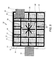
- Fig. 5 illustrates an FET array 52 which is similar to the FET array 18 of Fig. 4 with the addition of a gate driver network 54 integrated into, i.e., made a part of the array 52 and located at the central region thereof.
- the gate driver network 54 is centrally located so as to take advantage of the symmetrical layout provided by a signal distribution arrangement 56 having an X-shaped central portion with the ends thereof electrically connected to the gate terminals 14 of the four FETs comprising the gate driver network 54.
- Fig. 5 further illustrates a metallization region 58 which interconnects the source terminals of the FETs 10 by way of vias 60 of the gate drive network 54 and, if desired, may be part of the second metallization layer 40, shown in Fig.
- a contact pad (not shown) for the source terminals, as well as a contact pad for the drain terminals, of the FETs 10 of the gate driver network 48 needs to be provided in a manner as described for contact pads 50 and 48 of Fig. 3.
- the FETs 10 of Figs. 4 and 5, as well as those of Figs. 2 and 3, have a single gate contact so as to yield one effective gate resistance.
- the effective gate resistance may be further reduced by using a FET having four gate contact pads, as described with reference to Fig. 6.
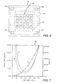
- Fig. 6 illustrates a FET 62 having four gate terminals 16A, 16B, 16C, 16D located in the four comers of the periphery of FET 62 and interconnected by the third metallization layer 42.
- the FET 62 further comprises a contact pad array 64 electrically connected to the second layer 40 which may be used to replace the source contact pad 50 of Figs. 4 and 5.
- HDI structures are advantageously employed to provide second and third level interconnect structures such as those illustrated in Fig. 6.
- the FET array 18 has the same breakdown voltage and/or power level of the individual FETs 10 mounted thereon. Actually, the breakdown voltage is determined by the FET 10 having the lowest breakdown voltage. The terms “breakdown voltage” and “power level” may be used herein in an interchangeable manner to describe the power switching parameters of the FETs 10 described herein.
- the total on-state resistance of the FET array 18 is the parallel combination of the on-state resistance of the individual FETs 10. Therefore, if sixteen individual FETs are used, as shown in Fig. 4, the total resistance of the FET array 18 is sixteen times lower than one FET 10, as are conduction losses, of the individual FETs 10.
- the gate switching capacitance of the array 18 is also sixteen times higher than that of the individual FET 10.
- the number of FETs 10 can be selected to provide an optimum balance between conduction (resistance) and switching (capacitance) losses. Further, this selectable number increases the yield of FETs 10 because it eliminates the need for fabricating one FET 10 having the desired conduction and switching losses. The selection of the number of FETs 10 that yields the desired conduction and switching losses associated with the gate resistance of the FETs 10 may be further described with reference to Fig. 7.
- Fig. 7 illustrates a family 66 of plots representative of the total FET power distribution as a function of FET area.
- the family 66 is comprised of plots 68, 70, and 72, wherein plots 68 and 70 represent the operational responses of off-the-shelf FET types 1RF150 and 1RF230, respectively, and wherein plot 72 represents the capacitance of a particular FET having a switching capability that exceeds 1 MHz.
- Fig. 7 has an X axis representative of chip size (mils) of the FET and two Y axes, with the first Y axis representative of resistance loss (watts) and with the second Y axis representative of capacitive loss (p f ).
- minimum power loss is a strong function of the FET size, and this minimum power loss depends upon voltage rating, switching frequency, and power level.
- the parameters illustrated in Fig. 7 may be selected in a manner so that the FET 10 or the FET arrays 18 and 52 provide an optimum arrangement with regard to on-resistance and switching capacitance. More particularly, the FET 10 may be selected to have a chip size of 50 mils (gradient of X axis of Fig. 7) and then the number of FET's 10 may be selected to correspond to any desired operational region with respect to plots 68, 70 and 72.
- One advantage of the selection of the number of FETs that determine the FET array is the ability to build large devices, not only large FET arrays, but also large MOS-gated arrays such as those comprised of IGBTs that operate at relatively low switching frequencies (10 KHz - 150 KHz) when compared to the FET 10 as described hereinabove having switching speeds of from 100 KHz to less than 10 MHz.
- Such selectable arrays provide an advantage because conduction losses tend to dominate for these switching frequencies.
- the practice of the present invention is equally applicable to MOS-FET power devices whose utilization, for example, is more fully described in U.S. Patent 5,384,691.
- exemplary building blocks may include over-temperature monitors, electrostatic discharge (ESD) damage protection, and current mirror devices.
- ESD electrostatic discharge
- Fig. 8 is composed of Figs. 8(a), 8(b), 8(c), and 8(d), that respectively illustrate (a) a gate tum-off configuration 74; (b) parallel FETs 76; (c) a current mirror 78; and (d) a gate driver configuration 80.
- Fig. 8(a) illustrates FETs Q1 and Q2, with Q2 being arranged as a gate tum-off FET which acts as a low resistance path to gate current during turn-off. The low impedance path is important when Q2 is tumed on.
- Fig. 8(b) illustrates the parallel arrangement provided by two FETs Q1 and Q2 arranged as shown therein.
- Fig. 8(c) illustrates a current mirror arrangement with the FET Q2 acting as a current mirror FET.
- the current mirror FET Q2 has an isolated or independent source contact which provides, for example, a representative sample of the total current flowing in the arrangement of Fig. 8(c). This sample can be used as part of a control loop.
- Fig. 8(d) shows a gate driver configuration wherein FET Q2 acts as a gate driver FET that may form part of the FET array 46 of Fig. 5.
- the FET arrays of Figs. 4 and 5 may each be treated as a self-contained device placed on a heat spreading substrate, such as that provided by the copper pad 22.
- FET 10 of Figs. 2 and 3 is a three terminal device (gate, source and drain) wherein all three terminals could be arranged on the same plane using a series of vias to bring all contacts to the same surface in a manner generally illustrated in Fig. 3. This has particular importance if the copper pad 22 has a thickness of about 40 mils, for example.
- the present invention advantageously provides for one or more FETs arranged in an array wherein the gate, source and drain terminals of all of the FETs are provided with electrical interconnections by a three layer metallization arrangement.
- the FET arrays may be selected so as to provide for the desired on-resistance and switching capacitance to serve the needs of a selectable power level.
- the present invention also provides several production advantages. First, only one-size FET needs to be produced, and the number of these FETs may be selected to provide a desired operational response for a particular power level. Second, the use of a building block (one-size FET) to provide a larger die increases the yield.
Landscapes
- Semiconductor Integrated Circuits (AREA)
- Internal Circuitry In Semiconductor Integrated Circuit Devices (AREA)
- Insulated Gate Type Field-Effect Transistor (AREA)
- Junction Field-Effect Transistors (AREA)
Applications Claiming Priority (2)
| Application Number | Priority Date | Filing Date | Title |
|---|---|---|---|
| US24485 | 1987-03-11 | ||
| US09/024,485 US5959357A (en) | 1998-02-17 | 1998-02-17 | Fet array for operation at different power levels |
Publications (2)
| Publication Number | Publication Date |
|---|---|
| EP0938138A2 true EP0938138A2 (fr) | 1999-08-25 |
| EP0938138A3 EP0938138A3 (fr) | 2003-08-20 |
Family
ID=21820831
Family Applications (1)
| Application Number | Title | Priority Date | Filing Date |
|---|---|---|---|
| EP99301160A Ceased EP0938138A3 (fr) | 1998-02-17 | 1999-02-17 | Rangée de FETs pour opération en niveaux de puissance différents |
Country Status (3)
| Country | Link |
|---|---|
| US (1) | US5959357A (fr) |
| EP (1) | EP0938138A3 (fr) |
| JP (1) | JP4424698B2 (fr) |
Cited By (4)
| Publication number | Priority date | Publication date | Assignee | Title |
|---|---|---|---|---|
| WO2002023631A3 (fr) * | 2000-09-13 | 2002-06-06 | Intel Corp | Couche d'accumulation directe sur un boitier de de encapsule dote d'une structure barriere d'humidite |
| EP1434268A3 (fr) * | 2002-12-26 | 2004-08-25 | Yamaha Hatsudoki Kabushiki Kaisha | Substrat électrique, module de puissance et entraíneur de moteur |
| US7078788B2 (en) | 2000-08-16 | 2006-07-18 | Intel Corporation | Microelectronic substrates with integrated devices |
| EP4513544A1 (fr) * | 2023-08-24 | 2025-02-26 | Shinko Electric Industries Co., Ltd. | Appareil à semi-conducteur |
Families Citing this family (34)
| Publication number | Priority date | Publication date | Assignee | Title |
|---|---|---|---|---|
| KR100230428B1 (ko) * | 1997-06-24 | 1999-11-15 | 윤종용 | 다층 도전성 패드를 구비하는 반도체장치 및 그 제조방법 |
| US6057779A (en) * | 1997-08-14 | 2000-05-02 | Micron Technology, Inc. | Method of controlling access to a movable container and to a compartment of a vehicle, and a secure cargo transportation system |
| US6356535B1 (en) * | 1998-02-04 | 2002-03-12 | Micron Technology, Inc. | Communication systems and methods of communicating |
| WO2000021126A1 (fr) * | 1998-10-05 | 2000-04-13 | Kulicke & Soffa Investments, Inc. | Protection de la surface des plots de connexion cuivre des semi-conducteurs |
| US6303423B1 (en) * | 1998-12-21 | 2001-10-16 | Megic Corporation | Method for forming high performance system-on-chip using post passivation process |
| US6965165B2 (en) | 1998-12-21 | 2005-11-15 | Mou-Shiung Lin | Top layers of metal for high performance IC's |
| US6936531B2 (en) | 1998-12-21 | 2005-08-30 | Megic Corporation | Process of fabricating a chip structure |
| US10973397B2 (en) | 1999-03-01 | 2021-04-13 | West View Research, Llc | Computerized information collection and processing apparatus |
| US8636648B2 (en) | 1999-03-01 | 2014-01-28 | West View Research, Llc | Endoscopic smart probe |
| JP4094174B2 (ja) | 1999-06-04 | 2008-06-04 | 株式会社ルネサステクノロジ | 半導体装置の製造方法 |
| US8065155B1 (en) | 1999-06-10 | 2011-11-22 | Gazdzinski Robert F | Adaptive advertising apparatus and methods |
| US7710273B2 (en) * | 1999-09-02 | 2010-05-04 | Round Rock Research, Llc | Remote communication devices, radio frequency identification devices, wireless communication systems, wireless communication methods, radio frequency identification device communication methods, and methods of forming a remote communication device |
| US6818545B2 (en) * | 2001-03-05 | 2004-11-16 | Megic Corporation | Low fabrication cost, fine pitch and high reliability solder bump |
| US7498196B2 (en) | 2001-03-30 | 2009-03-03 | Megica Corporation | Structure and manufacturing method of chip scale package |
| US7932603B2 (en) | 2001-12-13 | 2011-04-26 | Megica Corporation | Chip structure and process for forming the same |
| TW503496B (en) * | 2001-12-31 | 2002-09-21 | Megic Corp | Chip packaging structure and manufacturing process of the same |
| TW584950B (en) | 2001-12-31 | 2004-04-21 | Megic Corp | Chip packaging structure and process thereof |
| TW544882B (en) | 2001-12-31 | 2003-08-01 | Megic Corp | Chip package structure and process thereof |
| US6673698B1 (en) | 2002-01-19 | 2004-01-06 | Megic Corporation | Thin film semiconductor package utilizing a glass substrate with composite polymer/metal interconnect layers |
| JP3616605B2 (ja) * | 2002-04-03 | 2005-02-02 | 沖電気工業株式会社 | 半導体装置 |
| WO2003107422A1 (fr) * | 2002-06-13 | 2003-12-24 | 松下電器産業株式会社 | Dispositif a semi-conducteurs et son procede de fabrication |
| US7427024B1 (en) | 2003-12-17 | 2008-09-23 | Gazdzinski Mark J | Chattel management apparatus and methods |
| DE102004019447A1 (de) * | 2004-04-19 | 2005-11-10 | Siemens Ag | Vorrichtung, insbesondere intelligentes Leistungsmodul, mit planarer Verbindungstechnik |
| US7560808B2 (en) * | 2005-10-19 | 2009-07-14 | Texas Instruments Incorporated | Chip scale power LDMOS device |
| US20090015407A1 (en) * | 2007-07-13 | 2009-01-15 | Micron Technology, Inc. | Rifid tags and methods of designing rfid tags |
| US7777630B2 (en) * | 2007-07-26 | 2010-08-17 | Round Rock Research, Llc | Methods and systems of RFID tags using RFID circuits and antennas having unmatched frequency ranges |
| US8179232B2 (en) * | 2008-05-05 | 2012-05-15 | Round Rock Research, Llc | RFID interrogator with adjustable signal characteristics |
| US7852221B2 (en) * | 2008-05-08 | 2010-12-14 | Round Rock Research, Llc | RFID devices using RFID circuits and antennas having unmatched frequency ranges |
| US8712334B2 (en) | 2008-05-20 | 2014-04-29 | Micron Technology, Inc. | RFID device using single antenna for multiple resonant frequency ranges |
| US8053898B2 (en) * | 2009-10-05 | 2011-11-08 | Samsung Electronics Co., Ltd. | Connection for off-chip electrostatic discharge protection |
| US8847293B2 (en) * | 2012-03-02 | 2014-09-30 | Taiwan Semiconductor Manufacturing Company, Ltd. | Gate structure for semiconductor device |
| US9337163B2 (en) * | 2012-11-13 | 2016-05-10 | General Electric Company | Low profile surface mount package with isolated tab |
| US9006584B2 (en) * | 2013-08-06 | 2015-04-14 | Texas Instruments Incorporated | High voltage polymer dielectric capacitor isolation device |
| US9899484B1 (en) * | 2016-12-30 | 2018-02-20 | Texas Instruments Incorporated | Transistor with source field plates under gate runner layers |
Family Cites Families (11)
| Publication number | Priority date | Publication date | Assignee | Title |
|---|---|---|---|---|
| US4182023A (en) * | 1977-10-21 | 1980-01-08 | Ncr Corporation | Process for minimum overlap silicon gate devices |
| US4198250A (en) * | 1979-02-05 | 1980-04-15 | Intel Corporation | Shadow masking process for forming source and drain regions for field-effect transistors and like regions |
| US4343078A (en) * | 1979-03-05 | 1982-08-10 | Nippon Electric Co., Ltd. | IGFET Forming method |
| CA1198226A (fr) * | 1982-06-01 | 1985-12-17 | Eliezer Kinsbron | Methode de fabrication d'un dispositif semiconducteur |
| US4471524A (en) * | 1982-06-01 | 1984-09-18 | At&T Bell Laboratories | Method for manufacturing an insulated gate field effect transistor device |
| JPH06101652B2 (ja) * | 1987-02-12 | 1994-12-12 | 三菱電機株式会社 | バイアス回路 |
| US4783695A (en) * | 1986-09-26 | 1988-11-08 | General Electric Company | Multichip integrated circuit packaging configuration and method |
| US5384691A (en) * | 1993-01-08 | 1995-01-24 | General Electric Company | High density interconnect multi-chip modules including embedded distributed power supply elements |
| US5696403A (en) * | 1993-10-25 | 1997-12-09 | Lsi Logic Corporation | System having input-output drive reduction |
| US5455442A (en) * | 1993-11-17 | 1995-10-03 | Harris Corporation | COMFET switch and method |
| US5498556A (en) * | 1995-01-10 | 1996-03-12 | United Microelectronics Corp. | Metal-oxide-semiconductor field-effect transistor and its method of fabrication |
-
1998
- 1998-02-17 US US09/024,485 patent/US5959357A/en not_active Expired - Lifetime
-
1999
- 1999-02-04 JP JP02679799A patent/JP4424698B2/ja not_active Expired - Fee Related
- 1999-02-17 EP EP99301160A patent/EP0938138A3/fr not_active Ceased
Cited By (7)
| Publication number | Priority date | Publication date | Assignee | Title |
|---|---|---|---|---|
| US7078788B2 (en) | 2000-08-16 | 2006-07-18 | Intel Corporation | Microelectronic substrates with integrated devices |
| WO2002023631A3 (fr) * | 2000-09-13 | 2002-06-06 | Intel Corp | Couche d'accumulation directe sur un boitier de de encapsule dote d'une structure barriere d'humidite |
| US6713859B1 (en) | 2000-09-13 | 2004-03-30 | Intel Corporation | Direct build-up layer on an encapsulated die package having a moisture barrier structure |
| US7416918B2 (en) | 2000-09-13 | 2008-08-26 | Intel Corporation | Direct build-up layer on an encapsulated die package having a moisture barrier structure |
| EP1434268A3 (fr) * | 2002-12-26 | 2004-08-25 | Yamaha Hatsudoki Kabushiki Kaisha | Substrat électrique, module de puissance et entraíneur de moteur |
| US7119437B2 (en) | 2002-12-26 | 2006-10-10 | Yamaha Hatsudoki Kabushiki Kaisha | Electronic substrate, power module and motor driver |
| EP4513544A1 (fr) * | 2023-08-24 | 2025-02-26 | Shinko Electric Industries Co., Ltd. | Appareil à semi-conducteur |
Also Published As
| Publication number | Publication date |
|---|---|
| JPH11274370A (ja) | 1999-10-08 |
| JP4424698B2 (ja) | 2010-03-03 |
| EP0938138A3 (fr) | 2003-08-20 |
| US5959357A (en) | 1999-09-28 |
Similar Documents
| Publication | Publication Date | Title |
|---|---|---|
| US5959357A (en) | Fet array for operation at different power levels | |
| US5637922A (en) | Wireless radio frequency power semiconductor devices using high density interconnect | |
| US7639061B2 (en) | Semiconductor device and capacitance regulation circuit | |
| US5532512A (en) | Direct stacked and flip chip power semiconductor device structures | |
| JP7642714B2 (ja) | 半導体装置 | |
| JP4955078B2 (ja) | 半導体装置 | |
| JP3345241B2 (ja) | 半導体装置 | |
| WO1999065077A9 (fr) | Conditionnement a resistance reduite pour dispositifs a semi-conducteurs | |
| US20020096748A1 (en) | Back-to -back connected power semiconductor device package | |
| US12255191B2 (en) | Semiconductor device | |
| US20050194660A1 (en) | IGBT module | |
| US7019362B2 (en) | Power MOSFET with reduced dgate resistance | |
| WO2004049435A1 (fr) | Dispositif semi-conducteur a pinces pour raccordement sur des elements exterieurs | |
| US5366932A (en) | Semi-conductor chip packaging method and semi-conductor chip having interdigitated gate runners with gate bonding pads | |
| US5027192A (en) | Fast power semiconductor circuit | |
| US7042730B2 (en) | Non-isolated heatsink(s) for power modules | |
| JP2003197914A (ja) | 半導体装置 | |
| US20240421139A1 (en) | Module assembly of multiple semiconductor devices with insulating substrates | |
| US20020180036A1 (en) | Semiconductor device | |
| EP3748851B1 (fr) | Dispositif à semi-conducteur et agencement de semi-conducteur comprenant des dispositifs à semi-conducteur | |
| CN112951819A (zh) | 半导体器件模块及组装方法 | |
| JP7736907B2 (ja) | ターンオン/ターンオフ挙動のバランスのための非対称な集積集中ゲート抵抗器及び/又はパワー処理の向上のための複数の離間した集中ゲート抵抗器を有する半導体デバイス | |
| KR20060007014A (ko) | 캡슐화된 전력 반도체 조립체 | |
| KR101754923B1 (ko) | 고 전자이동도 트랜지스터 기반 전력 모듈 | |
| JP2000174201A (ja) | マルチチップモジュール型半導体装置 |
Legal Events
| Date | Code | Title | Description |
|---|---|---|---|
| PUAI | Public reference made under article 153(3) epc to a published international application that has entered the european phase |
Free format text: ORIGINAL CODE: 0009012 |
|
| AK | Designated contracting states |
Kind code of ref document: A2 Designated state(s): AT BE CH CY DE DK ES FI FR GB GR IE IT LI LU MC NL PT SE |
|
| AX | Request for extension of the european patent |
Free format text: AL;LT;LV;MK;RO;SI |
|
| RTI1 | Title (correction) |
Free format text: FET ARRAY FOR OPERATION AT DIFFERENT POWER LEVELS |
|
| PUAL | Search report despatched |
Free format text: ORIGINAL CODE: 0009013 |
|
| AK | Designated contracting states |
Designated state(s): AT BE CH CY DE DK ES FI FR GB GR IE IT LI LU MC NL PT SE |
|
| AX | Request for extension of the european patent |
Extension state: AL LT LV MK RO SI |
|
| 17P | Request for examination filed |
Effective date: 20040220 |
|
| 17Q | First examination report despatched |
Effective date: 20040329 |
|
| AKX | Designation fees paid |
Designated state(s): DE FR GB IT |
|
| 17Q | First examination report despatched |
Effective date: 20040329 |
|
| STAA | Information on the status of an ep patent application or granted ep patent |
Free format text: STATUS: THE APPLICATION HAS BEEN REFUSED |
|
| 18R | Application refused |
Effective date: 20120219 |