EP0938732B1 - Cellule electronique analogique, notamment destinee a etre implantee dans un circuit integre, et circuit integre comportant de telles cellules - Google Patents
Cellule electronique analogique, notamment destinee a etre implantee dans un circuit integre, et circuit integre comportant de telles cellules Download PDFInfo
- Publication number
- EP0938732B1 EP0938732B1 EP97945906A EP97945906A EP0938732B1 EP 0938732 B1 EP0938732 B1 EP 0938732B1 EP 97945906 A EP97945906 A EP 97945906A EP 97945906 A EP97945906 A EP 97945906A EP 0938732 B1 EP0938732 B1 EP 0938732B1
- Authority
- EP
- European Patent Office
- Prior art keywords
- cell
- terminal
- input
- output
- current conveyor
- Prior art date
- Legal status (The legal status is an assumption and is not a legal conclusion. Google has not performed a legal analysis and makes no representation as to the accuracy of the status listed.)
- Expired - Lifetime
Links
- 239000003990 capacitor Substances 0.000 claims abstract description 12
- 230000006870 function Effects 0.000 claims description 27
- 239000011159 matrix material Substances 0.000 claims description 11
- 230000002457 bidirectional effect Effects 0.000 claims description 6
- 230000001131 transforming effect Effects 0.000 claims description 2
- 238000012886 linear function Methods 0.000 claims 1
- 235000021183 entrée Nutrition 0.000 description 17
- 238000010586 diagram Methods 0.000 description 16
- 230000010287 polarization Effects 0.000 description 7
- 238000013528 artificial neural network Methods 0.000 description 3
- 230000006399 behavior Effects 0.000 description 3
- 238000005516 engineering process Methods 0.000 description 3
- 101000848724 Homo sapiens Rap guanine nucleotide exchange factor 3 Proteins 0.000 description 2
- 102100034584 Rap guanine nucleotide exchange factor 3 Human genes 0.000 description 2
- XUIMIQQOPSSXEZ-UHFFFAOYSA-N Silicon Chemical compound [Si] XUIMIQQOPSSXEZ-UHFFFAOYSA-N 0.000 description 2
- 238000001914 filtration Methods 0.000 description 2
- 230000010354 integration Effects 0.000 description 2
- 238000000034 method Methods 0.000 description 2
- 229910052710 silicon Inorganic materials 0.000 description 2
- 239000010703 silicon Substances 0.000 description 2
- 230000003068 static effect Effects 0.000 description 2
- 238000009795 derivation Methods 0.000 description 1
- 230000005611 electricity Effects 0.000 description 1
- 238000005265 energy consumption Methods 0.000 description 1
- 239000007943 implant Substances 0.000 description 1
- 230000001939 inductive effect Effects 0.000 description 1
- 238000003909 pattern recognition Methods 0.000 description 1
- 230000009711 regulatory function Effects 0.000 description 1
- 230000004044 response Effects 0.000 description 1
- 238000005070 sampling Methods 0.000 description 1
- 238000000926 separation method Methods 0.000 description 1
- 238000011282 treatment Methods 0.000 description 1
Images



Classifications
-
- G—PHYSICS
- G11—INFORMATION STORAGE
- G11C—STATIC STORES
- G11C27/00—Electric analogue stores, e.g. for storing instantaneous values
- G11C27/02—Sample-and-hold arrangements
- G11C27/024—Sample-and-hold arrangements using a capacitive memory element
Definitions
- the invention relates to the field of analog electronics. It aims more precisely a configurable elementary analog cell capable of ensuring transfer function determined.
- the invention also relates to an integrated circuit including a plurality of elementary cells networked to form a component programmable analog.
- EPAC Electronically Programmable Analog Array Circuit
- This type of component behaves like an analog network programmable in which the different signals which pass are discretized in view of their digital processing, then reconverted into analog signals. These components operate using switched capacitance technology. Their operating frequency is therefore relatively limited to 120 kHz. It is therefore impossible with such components to carry out filtering at frequencies high.
- a first problem which the invention therefore proposes to solve is that of the operating frequency limitation imposed by existing technology.
- the components of the EPAC type operate by producing digital treatments which therefore consume energy, whatever the value of the signal to be processed. This therefore prohibits the use of such components in applications requiring relative energy autonomy, such as example the realization of filtering of hearing aids.
- a second problem which the invention therefore proposes to solve is therefore that of electricity consumption, and as a corollary of energy autonomy such components.
- a third problem which the invention therefore proposes to solve is that the compactness of the elementary cells of an analog component programmable.
- the component described in the aforementioned document operates using a switched capacity technology ensuring a sampling of certain signals.
- switched capacities induces limitations in frequency of use as well as problems of non-linearity and noises.
- the invention overcomes all these drawbacks, and aims to produce a component programmable analog operating at high frequencies of the order of MHz, which has a low consumption, and satisfactory compactness.
- the invention therefore relates first of all to an analog electronic cell elementary, in particular intended to be installed in an integrated circuit analog programmable, and comprising an input terminal (E), a exits).
- the main ones can be produced analog functions.
- In playing jointly on the values of the capacitances of the resistors we can also get high pass, low pass, band pass or tape rejector.
- the structure of the elementary cell is completely analog, which allows it to operate at higher frequencies than those allowed with programmable analog components of the prior state which include digital processing.
- the reference potentials M 1 and M 2 are connected, so that the cell operates in common mode.
- the cell includes a second current conveyor allowing it to operate in differential mode.
- the output of the second current conveyor is connected to the reference potential M 2 and constitutes the negative terminal (S - ) of the differential output, while one of the inputs (X) of the second current conveyor is connected to the potential reference (M 1 ), and that the other input (Y) of the second current conveyor constitutes the negative terminal (E - ) of the differential input.
- this cell is bidirectional, and made up of two cells as described above, head to tail mounted, the input and output terminals of the first cell being connected respectively to the output and input terminals of the second cell.
- the resistances of the RC circuits connected to the various terminals of the current conveyors are adjustable electronically.
- one of the adjustable resistances measured between its two lower and upper terminals respectively is produced by the association of two transistors placed in parallel, and operating in ohmic regime, the gate of one of the transistors being brought to a control potential (+ V C ) relative to the lower terminal of the adjustable resistor, the gate of the other transistor being brought to the opposite control potential (-V C ) relative to the upper terminal of the adjustable resistor.
- the capacities of the RC circuits connected to the different current conveyor terminals are also adjustable.
- one of the resistors connected to the second current conveyor is adjustable and performed as described above.
- the current conveyors have controllable bias sources.
- the two polarization sources are controlled simultaneously to give the current conveyors an open circuit or short circuit function.
- a properly controlled cell can serve as a bypass, or to the opposite of an open switch between adjacent cells.
- the two sources of polarization of the conveyor are controlled independently of each other, so that implement non-linear analog functions such as rectification, multiplication, logarithm and exponential.
- analog elementary cells implanted inside the analog circuit are carried out as described previously.
- the invention also covers alternative embodiments using cells not comprising no current conveyor, but equivalent means, provided that the spirit of the invention is respected, that is to say that the cells are purely analog, and contain resistive and capacitive components of value adjustable electronically.
- the means for adjusting the values of each capacitive and resistive components are constituted by a memory erasable analog (EEPROM), directly connected to the resistive elements and capacitive, and to the sources of bias of the current conveyors of the cells elements of the network.
- EEPROM memory erasable analog
- the different elementary cells are intended to be connected to the network.
- the different cells elementary are interconnected according to a matrix network.
- the different cells connected together form a mesh.
- the different elementary cells can be interconnected according to a tree, systolic or connectionist network, thereby approaching the topology of a neural network.
- Figure 1 is a block diagram showing an elementary cell unidirectional operating in common mode.
- Figure 2 is a block diagram showing an elementary cell unidirectional operating in differential mode.
- Figures 3 and 4 are block diagrams showing a cell bidirectional elementary operating respectively in common mode and in differential mode.
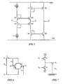
- Figure 5 is an electronic diagram showing the internal structure of a conventional current conveyor.
- Figure 6 is an electrical diagram showing the realization of a resistance adjustable according to the invention.
- Figure 7 is an electronic diagram showing a preferred form of realization of an adjustable resistance.
- Figures 8 and 9 are electronic diagrams illustrating two embodiments adjustable capacity according to the invention.
- Figure 10 is a diagram showing a bidirectional cell operating as a gyrator.
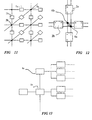
- Figure 11 is a block diagram illustrating different cells according to the invention mounted in a matrix network.
- Figure 12 is a block diagram illustrating different cells operating in differential mode mounted in a matrix network.
- Figure 13 is a block diagram showing the different cells according to the invention interconnected according to a tree network.
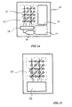
- Figure 14 is a block diagram showing the different elements components an integrated circuit according to the invention.
- Figure 15 is a block diagram showing a variant of Figure 8 using analog memory.
- the invention relates on the one hand, to an elementary cell analog programmable, and on the other hand, an integrated circuit comprising a plurality of elementary cells interconnected in a network.
- Such an elementary cell (1) essentially consists of a current conveyor structure (CC) and two parallel RC circuits (R 1, C 1 , R 2 , C 2 ) charging an input (X) and the output (Z) of the current conveyor (CC).
- the current conveyor structure known per se, will not be described here in detail. However, it can in particular be produced according to an electronic diagram forming the subject of FIG. 5, in which the reference elements M 1 to M 8 are MOSFET transistors and the current sources I 0 are polarization sources.
- the transfer function a plurality of transfer functions of order 0 or 1. It is possible to cite by way of example and without limitation the functions of follower, inverting amplifier, integrator, derivator, high-pass filter, low-pass, band-pass or band-rejector.
- such a structure consists of two current conveyors (CC 1 and CC 2 ).
- the first current conveyor (CC 1 ) has an input (Y 1 ) connected to the positive terminal (E + ) of the cell, the output (Z 1 ) of the current conveyor (CC 1 ) is connected to the upper terminal ( S + ) of the cell output.
- the second current conveyor (CC 2 ) has an input (X 2 ) directly connected to the lower terminal (E - ) of the cell input while the output (Z 2 ) of the conveyor (CC 2 ) is connected to the negative terminal (S - ) of the cell output.
- the two conveyors (CC 1 and CC 2 ) are connected by two characteristic RC circuits (RC E , RC S ).
- a first circuit connects the inputs (X 1 ) and (Y 2 ) respectively of the first current conveyor (CC 1 ) of the second (CC 2 ).
- a second RC circuit (RC S ).
- This architecture corresponds to the symmetrization with respect to a fictitious average potential of a basic cell as illustrated in FIG. 1.
- one of the inputs Y 3 of the first current conveyor CC 3 is connected to the output Z 4 of the second conveyor of CC 4 , these two points being themselves connected to a terminal ES 1 serving as input / output of the global cell (1).
- the output Z 3 of the first current conveyor CC 3 is connected to the input X 4 of the second current conveyor CC 4 , these two points also being connected to a second input / output terminal ES 2 .
- the inputs X 3 and X 4 of the current conveyors CC 3 , CC 4 are connected by two RC circuits to a common potential (M).
- the outputs of each current conveyor are also each connected to an RC circuit itself connected to the common potential (M).
- each of the RC circuits connected to input / output terminals of each cell is shared with the adjacent cells.
- cells in differential version can be mounted head to tail to be bidirectional.
- two cells (2) equivalent to those shown in Figure 2 are mounted head to tail, the outputs (S 1 + ) and (S 1 - ) of the first cell of A being connected, respecting the polarity at the inputs (E 2 + ) and (E 2 - ) of cell 2B.
- the outputs (S 2 + ) and (S 2 - ) of cell 2B are connected to the inputs (E 1 + ) and (E 1 - ) of cell 2A.
- each of the components of the different RC circuits connected to the current conveyors are electronically adjustable, i.e. their value can be controlled by a control signal.
- the resistors are constituted as illustrated in FIG. 6. More precisely, the circuit exhibits behavior equivalent to that of a resistance in the sense that the current I R which passes through it is proportional to the voltage V R measured between its positive R + and negative R - terminals. In practice, this resistive behavior is obtained by the association of two MOS transistors (T 1 , T 2 ) mounted in parallel, and polarized in ohmic regime.
- the resistance value is adjusted by the control potential (V C ) applied to the gates of each of these transistors (T).
- the first transistor (T 1 ) sees its gate (G 1 ) carried a potential V C relative to the lower terminal R - of the resistance.
- the gate (G 2 ) of the other transistor (T 2 ) is brought to the potential -V C with respect to the upper terminal R + of the resistor.
- successive ranges are chosen which form calibers, by example from 1 k ⁇ to 10 k ⁇ , then from 10 to 100 k ⁇ , and from 100 k ⁇ to 1 M ⁇ .
- the frequency response to the control signal of such a resistance is fast, and higher than 10 MHz.
- the resistance can be obtained according to the assembly object of FIG. 7.
- This assembly consists of two MOS transistors (T 3 , T 4 ) connected in series, one of the transistors (T 3 ) being connected to the positive power source (Vdd), while the other transistor (T 4 ) has one of its terminals connected to the negative power source (Vss).
- the common point of these two transistors constitutes the positive terminal of the equivalent resistance, the common potential (M) constituting the negative terminal of the equivalent resistance.
- the resistance value is adjusted by the control potential (Vn, Vp) applied to the gates of each of the transistors.
- the first transistor (T 3 ) has its gate (G 3 ) brought to the potential (Vn) relative to the lower terminal (R - ) of the resistor.
- the gate (G 2 ) of the other transistor (T 4 ) is brought to the potential (Vp) also with respect to the lower terminal of the resistor.
- the resistance value is then given by: 1 2. ⁇ .Cox. W L . ( V not - V Your ) ., with the same conventions as for the form described above.
- the impedance of such a circuit measured between the terminals C1 + and C1 - is therefore equal to that of the fixed capacitance C multiplied by the gain of the current amplifier, ie R1 / R2.
- This gain is adjusted by the use of one of the two adjustable resistors R 1 or R 2 , installed in accordance with one of the variable resistance diagrams described above.
- the adjustable capacity is produced according to a second architecture illustrated in FIG. 9.
- this adjustable capacity is based on a principle of capacitive multiplier based on current conveyor.
- the current conveyor (CC 7 ) has an input connected (Y 7 ) to the upper terminal (C 2 + ) of the equivalent adjustable capacity.
- the other input (X 7 ) of the current conveyor (CC 7 ) is connected to the common potential (M) via a resistor (R 71 ) of fixed value.
- the output (Z 7 ) of the current conveyor is connected on the one hand, to the common potential (M) via an adjustable resistance (R 72 ) and on the other hand, to the input (Y 7 ) of the current conveyor, i.e. the upper limit of the adjustable capacity (C 2 + ).
- the internal impedances of the cells are negligible and the apparent impedance of such a structure, between the terminals (C 1 + , C 1 - ) therefore corresponds to that of the fixed capacitance (C) multiplied by a gain adjustable according to the value of R 71 or R 72 .
- variable capacities are obtained in a range from 10 picoFarads to 4 nanoFarads.
- the current conveyor structures have at least two sources of polarization.
- a bidirectional cell as illustrated in FIG. 3, can also have a gyrator type second order transfer function.
- FIG. 10 illustrates such a cell in which the current conveyors have been shown one behind the other to facilitate understanding. More specifically, the RC circuit connected to the input terminal (29) of the cell, consists only of a single capacitor. The resistance R 9 in series with the input Y 8 of the current conveyor (8) corresponds to the internal resistance of the input (Y 8 ) of the current conveyor. The input (X 8 ) of the current conveyor (CC 8 ) is connected to the common potential (M). The RC circuit connected to the input (X 9 ) of the current conveyor (CC 9 ) consists only of a resistor (R 10 ).
- the RC circuit connected to the output (S) of the cell, that is to say to the input (Y 9 ) of the current conveyor (CC 9 ) is made up of a single capacity (C 10 ).
- the invention also relates to an electronic circuit built-in analog programmable.
- a programmable analog circuit essentially presents a plurality of purely elementary cells analog interconnected to each other in the form of an analog network.
- Each of the cells notably has resistive and capacitive components of adjustable value enabling each cell to be given simple transfers, that is to say of order 0 or 1.
- the association of these different cells between them gives the network a global transfer function complex, and resulting from the association of elementary transfer functions.
- the integrated circuit comprises means to adjust the sizes of each component according to predetermined values capacitive and / or resistive.
- the different elementary cells (1.a, 1.b) are interconnected in the form of a network matrix.
- this network comprises a plurality of nodes (5a, 5b) forming a matrix grid.
- the different adjacent nodes are each connected by elementary cells.
- the different cells connected at the level of a common node share one of the RC circuits connected at the output of one of current conveyors.
- Figure 12 illustrates the same type of network topology with differential cells.
- the RC circuits connecting the output terminals of a differential cell are shared at the level of the two (6a, 6b) of such a network.
- the topology in the form of a matrix network makes it possible in particular to treat advantageously the cases where several signals must be processed in parallel, then integrated into feedback loops.
- the links at the level of each of the nodes allow elementary cells to be used to perform functions of summation of signals.
- the matrix topology proves to be advantageous in the application to prototyping and / or implementation of analog functions. It also allows to process multichannel analog functions, i.e. using this parallelism.
- the cells can be organized under form of a tree network as illustrated in figure 13.
- Such a topology can give rise to an operation of the “neural network” type.
- the elementary structure of a cell allows to realize between input and output a short circuit or an open circuit, or a function of programmable transfer from input to output or vice versa.
- Interconnection such cells together make it possible for signal processing, speech processing and recognition, image processing and pattern recognition, operations treatable by structures organized in neural networks.
- the operations thus treatable are for example correlation, matrix self-organization, classification, learning and self-learning ... etc.
- the cell structure according to the invention therefore adapts well to matrix, arborescent, systolic, connectionist or other.
- the network (15) of elementary cells (12) can be controlled as illustrated in Figure 14.
- the integrated circuit (14) therefore has a network (15) of elementary cells and control means constituted by a memory digital (16) containing the information corresponding to the values of the capacitive and resistive elements, as well as the state of the different sources of polarization of each of the elementary cells.
- This memory (16) can be programmed in a manner known per se.
- This memory (16) is associated with a logic control unit (17) capable of select the different information contained in the digital memory (16).
- This logic control unit (17) supplies a converter digital / analog (18) to transform digital information into signals analog corresponding in particular to the control voltages of the different adjustable resistances and capacities described above.
- Converter digital / analog (18) feeds an analog multiplexer (19) which switches the analog signal thus created in the direction of the cell (12), and more precisely of the variable resistance or target polarization source.
- a memory analog (20) directly supplies the various adjustable components of each cell, without the need for a multiplexer or digital to analog converter.
- a programmable analog component according to the invention has many applications. It can in particular be used to carry out very small analog filter elements, such as hearing aids. It can also be used to interface sensors measure or provide regulatory functions.
Landscapes
- Networks Using Active Elements (AREA)
- Semiconductor Integrated Circuits (AREA)
- Design And Manufacture Of Integrated Circuits (AREA)
- Analogue/Digital Conversion (AREA)
Description
- une structure de convoyeur de courant présentant deux entrées (X,Y) et une sortie (Z), une des entrées (Y) étant reliée à la borne d'entrée (E) de la cellule, la sortie (Z) étant reliée à la borne de sortie (S) de la cellule ;
- deux circuits RC parallèles (R1,C1 ;R2,C2) connectés chacun d'une part respectivement à un potentiel de référence (M1, M2), et d'autre part, respectivement à l'entrée libre (X) du convoyeur de courant, et à la borne de sortie (S) de la cellule, les valeurs des résistances et capacités (R1,C1 ;R2,C2) étant réglables par voie électronique à des valeurs prédéterminées pour conférer à la cellule une fonction de transfert d'ordre 0 ou 1.

F(s) = K × 1 + sτ1 / 1 + sτ2 où K représente le gain statique, τ1 et τ2 correspondant aux différentes fréquences de coupures des filtrés ainsi réalisés.
- un premier convoyeur de courant monté en suiveur, dont une entrée est reliée à la borne supérieure (C1 +) de la capacité réglable ;
- un second convoyeur de courant monté en amplificateur de courant,
dont :
- une entrée est reliée à la sortie du premier convoyeur de courant et à une première résistance (RC1) elle-même reliée au potentiel commun (M),
- l'autre entrée est reliée à une seconde résistance (RC2), elle-même reliée au potentiel commun (M),
- une capacité fixe (C) dont une borne est reliée à la borne inférieure de la capacité réglable (C1 -) et dont l'autre borne est conjointement reliée à la sortie du deuxième convoyeur de courant et à l'entrée libre du premier convoyeur de courant.
- un convoyeur de courant monté en amplificateur de courant dont :
- une entrée (X) est reliée à une première résistance, elle-même reliée au potentiel commun,
- la sortie (Z) est reliée à une seconde résistance, elle-même reliée au potentiel commun,
- l'entrée (Y) est reliée à la borne supérieure de la capacité réglable.
- une capacité fixe dont une borne est reliée à la borne supérieure de la capacité réglable, et dont l'autre borne est reliée à la sortie (Z) du convoyeur de courant.
- une pluralité de cellules élémentaires analogiques selon l'invention, interconnectées les unes aux autres pour former un réseau analogique, chacune des cellules comportant des composants actifs et des composants résistifs et capacitifs de valeur réglable pour conférer à chaque cellule une fonction de transfert d'ordre 0 ou 1.;
- des moyens pour régler selon des valeurs prédéterminées les grandeurs de chaque composant capacitif et/ou résistif.
- une mémoire numérique contenant des informations numériques correspondant aux valeurs prédéterminées des éléments capacitifs et résistifs ainsi qu'à l'état des sources de polarisation ;
- un convertisseur numérique/analogique transformant en valeur analogique les données de la mémoire numérique ;
- un multiplexeur analogique relié au convertisseur, et apte à alimenter les éléments résistifs et capacitifs, et les sources de polarisation des convoyeurs de courant des cellules élémentaires du réseau.
- une entrée (Y) de ce convoyeur de courant (CC) est reliée à la borne d'entrée (E) de la cellule ;
- l'autre entrée (X) du convoyeur de courant est reliée à un circuit RC parallèle (R1, C1) lui-même connecté au potentiel commun (M);
- la sortie (Z) du convoyeur de courant est reliée d'une part, à la sortie (S) de la cellule, et d'autre part, à un second circuit RC parallèle (R2, C2) lui-même également connecté au potentiel commun (M).
- K correspond au gain statique, c'est-à-dire à R2/R1,
- les valeurs τ1 et τ2 correspondent respectivement aux constantes de temps des circuits R1, C1 et R2, C2
- µ est la mobilité,
- Cox est la capacité surfacique d'oxyde de grille,
- W est la largeur du canal du transistor,
- VT est la tension de seuil du transistor
- un premier convoyeur de courant CC5:
- monté en suiveur, dont une entrée X5 est reliée à la borne supérieure (C1 +) de la capacité réglable ;
- un second convoyeur de courant CC6 monté en amplificateur de courant,
dont :
- une entrée Y6 est reliée à la sortie Z5 du premier convoyeur de courant CC5 et à une première résistance (RC1) elle-même reliée au potentiel commun (M),
- l'autre entrée X6 est reliée à une seconde résistance (RC2), elle-même reliée au potentiel commun (M),
- une capacité fixe (C) dont une borne est reliée à la borne inférieure de la capacité réglable (C1 -) et dont l'autre borne est conjointement reliée à la sortie Z6 du deuxième convoyeur de courant et à l'entrée libre Y5 du premier convoyeur de courant .
- l'unicité de la structure de cellules de base pour assurer de multiples fonctions de transfert ;
- une densité relativement élevée permettant typiquement d'implanter cent cellules élémentaires dans une surface de 4 mm2 ;
- une consommation énergétique fonction uniquement du nombre de cellules utilisées ;
- une très large bande passante due à l'utilisation d'une cellule purement analogique.
Claims (15)
- Cellule électronique analogique élémentaire unidirectionnelle, notamment destinée à être implantée dans un circuit intégré analogique programmable, et comportant une borne d'entrée (E), une borne de sortie (S) caractérisée en ce qu'elle comporte :une structure de convoyeur de courant présentant deux entrées (X,Y) et une sortie (Z), une des entrées (Y) étant reliée à la borne d'entrée (E) de la cellule, la sortie (Z) étant reliée à la borne de sortie (S) de la cellule ;deux circuits RC parallèles (R1,C1 ;R2,C2) connectés chacun d'une part respectivement à un potentiel de référence (M1, M2), et d'autre part, respectivement à l'entrée libre (X) du convoyeur de courant, et à la borne de sortie (S) de la cellule, les valeurs des résistances et capacités (R1,C1 ;R2,C2) étant réglables par voie électronique à des valeurs prédéterminées pour conférer à la cellule une fonction de transfert d'ordre 0 ou 1.
- Cellule électronique analogique élémentaire unidirectionnelle selon la revendication 1, caractérisée en ce que les potentiels de référence M1 et M2 sont connectés, de manière que la cellule fonctionne en mode commun.
- Cellule électronique analogique élémentaire unidirectionnelle selon la revendication 1, caractérisée en ce qu'elle comporte un second convoyeur de courant lui permettant de fonctionner en mode différentiel, la sortie (Z) du second convoyeur de courant étant reliée au potentiel de référence M2 et constituant la borne négative (S-) de la sortie différentielle, une des entrées (X) du second convoyeur de courant étant reliée au potentiel de référence (M1), l'autre entrée (Y) du second convoyeur de courant constituant la borne négative E- de l'entrée différentielle.
- Cellule électronique analogique élémentaire bidirectionnelle, notamment destinée à être implantée dans un circuit intégré analogique programmable, caractérisée en ce qu'elle est constituée de deux cellules selon l'une des revendications 1 à 3, montées tête-bêche, les bornes d'entrée (E1) et de sortie (S1) de la première cellule étant reliées respectivement aux bornes de sortie (S2) et d'entrée (E2) de la seconde cellule.
- Cellule selon l'une des revendications 1 à 4, caractérisée en ce qu'une des résistances réglables (R1, R2), mesurées entre ses deux bornes respectivement inférieure (R1 -), et supérieure (R1 +), est réalisée par l'association de deux transistors mis en parallèle, et fonctionnant en régime ohmique, la grille d'un des transistors étant portée à un potentiel (+VC) de commande par rapport à la borne inférieure (R1 -) de la résistance réglable, la grille de l'autre transistor étant portée au potentiel de commande opposé (-VC) par rapport à la borne supérieure (R1 +) de la résistance réglable.
- Cellule selon l'une des revendications 1 ou 4, caractérisée en ce que l'une des résistances réglables (R1, R2), mesurées entre ses deux bornes respectivement inférieure (R1 -), et supérieure (R1 +), est réalisée par l'association de deux transistors mis en série, et fonctionnant en régime ohmique et de tensions de seuil (VTOM, VTOP) la borne d'un des transistors (T3) étant reliée à l'alimentation positive (Vdd), une des bornes de l'autre transistor (T4) étant reliée à l'alimentation négative (Vss), le point commun entre les deux transistors (T3, T4) constituant la borne positive (R1 +) de la résistance régable, la grille du transistor (T4) étant portée à un potentiel (Vn) de commande, la grille de l'autre transistor étant portée à un potentiel de commande (Vp) tel Vn - Vton = Vp - Vtop.
- Cellule selon l'une des revendications 1 à 6, caractérisée en ce que :la capacité réglable, mesurée entre ses bornes respectivement supérieure (C1 +) et inférieure (C1 -) est constituée par :un premier convoyeur de courant monté en suiveur, dont une entrée est reliée à la borne supérieure (C1 +) de la capacité réglable ;un second convoyeur de courant monté en amplificateur de courant, dont :une entrée est reliée à la sortie du premier convoyeur de courant et à une première résistance (RC1) elle-même reliée au potentiel commun (M),l'autre entrée est reliée à une seconde résistance (RC2), elle-même reliée au potentiel commun (M),une capacité fixe (C) dont une borne est reliée à la borne inférieure de la capacité réglable (C1 -) et dont l'autre borne est conjointement reliée à la sortie du deuxième convoyeur de courant et à l'entrée libre du premier convoyeur de courant ;et en ce qu'une des résistances (RC1, RC2) reliées au second convoyeur de courant est réglable et réalisée selon la revendication 3.
- Cellule selon l'une des revendications 1 à 6, caractérisée en ce que la capacité réglable, mesurée entre ses bornes respectivement supérieure (C1 +) et inférieure (C1 -) est constituée par :un convoyeur de courant monté en amplificateur de courant dont :une entrée (X) est reliée à une première résistance (R1), elle-même reliée au potentiel commun (M),la sortie (Z) est reliée à une seconde résistance (R2), elle-même reliée au potentiel commun (M),l'entrée (Y) est reliée à la borne supérieure (C1 +) de la capacité régable.une capacité fixe (C ) dont une borne est reliée à la borne supérieure (C1+) de la capacité réglable, et dont l'autre borne est reliée à la sortie (Z) du convoyeur de courant.
- Cellule selon l'une des revendications 1 à 8, caractérisée en ce que les convoyeurs de courant présentent des sources de polarisation (I0) commandée simultanément pour conférer à la cellule une fonction de circuit ouvert ou de court-circuit.
- Cellule selon l'une des revendications 1 à 8, caractérisée en ce que les convoyeurs de courant présentent des sources de polarisation (I0) commandées indépendamment pour conférer à la cellule une fonction non linéaire.
- Circuit électronique intégré analogique programmable, caractérisé en ce qu'il comporte :une pluralité de cellules élémentaires analogiques réalisées selon une des revendications 1 à 10, interconnectées les unes aux autres pour former un réseau analogique, chacune des cellules comportant des composants actifs et des composants résistifs et capacitifs de valeur réglable pour conférer à chaque cellule une fonction de transfert d'ordre 0 ou 1 ;des moyens pour régler selon des valeurs prédéterminées les grandeurs de chaque composant capacitif et/ou résistif.
- Circuit intégré électronique analogique programmable selon la revendication 11, caractérisé en ce que les moyens pour régler à des valeurs prédéterminées les grandeurs de chaque composant capacitif et/ou résistif sont constitués par :une mémoire numérique (16) contenant des informations numériques correspondant aux valeurs prédéterminées des éléments capacitifs et résistifs ainsi qu'à l'état des sources de polarisation ;un convertisseur numérique/analogique (18) transformant en valeur analogique les données de la mémoire numérique ;un multiplexeur analogique (19) relié au convertisseur (18), et apte à alimenter les éléments résistifs et capacitifs, et les sources de polarisation des convoyeurs de courant des cellules élémentaires (12) du réseau (15).
- Circuit intégré électronique analogique programmable selon l'une des revendications 11 ou 12, caractérisé en ce que les moyens pour régler à des valeurs prédéterminées les valeurs de chaque composants capacitifs et résistifs sont constitués par une mémoire analogique effaçable (EEPROM) (20), directement reliée aux éléments résistifs et capacitifs, et aux sources de polarisation des convoyeurs de courant des cellules élémentaires (12) du réseau (15).
- Circuit intégré électronique analogique programmable selon l'une des revendications 11 à 13, caractérisé en ce que les différentes cellules élémentaires (2) sont interconnectées selon un réseau matriciel.
- Circuit intégré électronique analogique programmable selon l'une des revendications 11 à 13, caractérisé en ce que les différentes cellules élémentaires (2) sont interconnectées selon un réseau arborescent.
Applications Claiming Priority (3)
| Application Number | Priority Date | Filing Date | Title |
|---|---|---|---|
| FR9614105A FR2755788B1 (fr) | 1996-11-14 | 1996-11-14 | Cellule electronique analogique, notamment destinee a etre implantee dans un circuit integre, et circuit integre comportant de telles cellules |
| FR9614105 | 1996-11-14 | ||
| PCT/FR1997/002026 WO1998021726A1 (fr) | 1996-11-14 | 1997-11-12 | Cellule electronique analogique, notamment destinee a etre implantee dans un circuit integre, et circuit integre comportant de telles cellules |
Publications (2)
| Publication Number | Publication Date |
|---|---|
| EP0938732A1 EP0938732A1 (fr) | 1999-09-01 |
| EP0938732B1 true EP0938732B1 (fr) | 2001-07-11 |
Family
ID=9497776
Family Applications (1)
| Application Number | Title | Priority Date | Filing Date |
|---|---|---|---|
| EP97945906A Expired - Lifetime EP0938732B1 (fr) | 1996-11-14 | 1997-11-12 | Cellule electronique analogique, notamment destinee a etre implantee dans un circuit integre, et circuit integre comportant de telles cellules |
Country Status (5)
| Country | Link |
|---|---|
| EP (1) | EP0938732B1 (fr) |
| AT (1) | ATE203122T1 (fr) |
| DE (1) | DE69705634T2 (fr) |
| FR (1) | FR2755788B1 (fr) |
| WO (1) | WO1998021726A1 (fr) |
Families Citing this family (4)
| Publication number | Priority date | Publication date | Assignee | Title |
|---|---|---|---|---|
| US6701340B1 (en) | 1999-09-22 | 2004-03-02 | Lattice Semiconductor Corp. | Double differential comparator and programmable analog block architecture using same |
| US6362684B1 (en) | 2000-02-17 | 2002-03-26 | Lattice Semiconductor Corporation | Amplifier having an adjust resistor network |
| US6424209B1 (en) | 2000-02-18 | 2002-07-23 | Lattice Semiconductor Corporation | Integrated programmable continuous time filter with programmable capacitor arrays |
| US9582687B2 (en) | 2015-05-15 | 2017-02-28 | King Fahd University Of Petroleum And Minerals | Reconfigurable integrator/differentiator circuit using current follower based simulated inductor |
Family Cites Families (2)
| Publication number | Priority date | Publication date | Assignee | Title |
|---|---|---|---|---|
| GB9007492D0 (en) * | 1990-04-03 | 1990-05-30 | Pilkington Micro Electronics | Semiconductor integrated circuit |
| US5124666A (en) * | 1991-03-04 | 1992-06-23 | Industrial Technology Research Institute | CMOS current convevor and its filter applications |
-
1996
- 1996-11-14 FR FR9614105A patent/FR2755788B1/fr not_active Expired - Fee Related
-
1997
- 1997-11-12 WO PCT/FR1997/002026 patent/WO1998021726A1/fr not_active Ceased
- 1997-11-12 EP EP97945906A patent/EP0938732B1/fr not_active Expired - Lifetime
- 1997-11-12 DE DE69705634T patent/DE69705634T2/de not_active Expired - Fee Related
- 1997-11-12 AT AT97945906T patent/ATE203122T1/de not_active IP Right Cessation
Also Published As
| Publication number | Publication date |
|---|---|
| FR2755788A1 (fr) | 1998-05-15 |
| EP0938732A1 (fr) | 1999-09-01 |
| DE69705634T2 (de) | 2001-10-31 |
| DE69705634D1 (de) | 2001-08-16 |
| WO1998021726A1 (fr) | 1998-05-22 |
| FR2755788B1 (fr) | 1998-12-31 |
| ATE203122T1 (de) | 2001-07-15 |
Similar Documents
| Publication | Publication Date | Title |
|---|---|---|
| EP0030173B1 (fr) | Filtre à capacités commutées à transfert de charges | |
| EP0028960B1 (fr) | Matrice de détection d'un rayonnement électromagnétique et intensificateur d'images radiologiques comportant une telle matrice | |
| FR2532115A1 (fr) | Circuit comprenant un element a transconductance variable | |
| EP0011556B1 (fr) | Filtre à transfert de charges électriques, programmable numériquement | |
| FR2558659A1 (fr) | Circuit de polarisation d'un transistor a effet de champ | |
| EP0562905A1 (fr) | Circuit à retard variable | |
| EP2131494A1 (fr) | Circuit à capacités commutées à consommation réduite | |
| EP0901227A1 (fr) | Circuit à retard variable | |
| FR2716052A1 (fr) | Dispositif d'ajustement d'une fréquence de coupure d'un filtre, et filtre comportant un tel dispositif. | |
| EP0810728A1 (fr) | Filtre audio analogique pour fréquences aigues | |
| EP0905852A1 (fr) | Circuit de protection associable à un filtre | |
| EP3457566A1 (fr) | Dispositif modifiant la valeur d'impedance d'une resistance de reference | |
| EP1647091B1 (fr) | Amplificateur de tension a faible consommation | |
| WO1998021726A1 (fr) | Cellule electronique analogique, notamment destinee a etre implantee dans un circuit integre, et circuit integre comportant de telles cellules | |
| EP2553623B1 (fr) | Circuit électronique analogique de traitement d'un signal lumineux, système et procédé de traitement correspondants | |
| EP0603070B1 (fr) | Procédé et dispositif pour la convolution analogique d'images | |
| EP0076737B1 (fr) | Intégrateur symétrique et application à un filtre | |
| FR3035290A1 (fr) | Carte electronique et systeme d'acquisition et de generation de signaux correspondant, comprenant un ou des commutateurs matriciels numeriques programmables | |
| EP0917288B1 (fr) | Cellule comportant une pseudo-capacité notamment pour rétine artificielle | |
| EP0129470B1 (fr) | Dispositif photosensible à l'état solide | |
| FR2582170A1 (fr) | Dipole auto-adaptatif | |
| EP3299991B1 (fr) | Circuit sommateur | |
| EP1146732B1 (fr) | Dispositif de conversion d'un photosignal en tension dans les senseurs d'images à intégrateurs déportés | |
| FR2478906A1 (fr) | Gyrateur a un seul amplificateur | |
| EP0021910A1 (fr) | Mosaique de détecteurs de rayonnement lue par un dispositif semiconducteur, et système de prise de vues comportant une telle mosaique |
Legal Events
| Date | Code | Title | Description |
|---|---|---|---|
| PUAI | Public reference made under article 153(3) epc to a published international application that has entered the european phase |
Free format text: ORIGINAL CODE: 0009012 |
|
| 17P | Request for examination filed |
Effective date: 19990506 |
|
| AK | Designated contracting states |
Kind code of ref document: A1 Designated state(s): AT BE CH DE ES FR GB IE IT LI PT |
|
| 17Q | First examination report despatched |
Effective date: 19991022 |
|
| GRAG | Despatch of communication of intention to grant |
Free format text: ORIGINAL CODE: EPIDOS AGRA |
|
| GRAG | Despatch of communication of intention to grant |
Free format text: ORIGINAL CODE: EPIDOS AGRA |
|
| GRAH | Despatch of communication of intention to grant a patent |
Free format text: ORIGINAL CODE: EPIDOS IGRA |
|
| GRAH | Despatch of communication of intention to grant a patent |
Free format text: ORIGINAL CODE: EPIDOS IGRA |
|
| GRAA | (expected) grant |
Free format text: ORIGINAL CODE: 0009210 |
|
| AK | Designated contracting states |
Kind code of ref document: B1 Designated state(s): AT BE CH DE ES FR GB IE IT LI PT |
|
| PG25 | Lapsed in a contracting state [announced via postgrant information from national office to epo] |
Ref country code: IE Free format text: LAPSE BECAUSE OF FAILURE TO SUBMIT A TRANSLATION OF THE DESCRIPTION OR TO PAY THE FEE WITHIN THE PRESCRIBED TIME-LIMIT Effective date: 20010711 Ref country code: AT Free format text: LAPSE BECAUSE OF FAILURE TO SUBMIT A TRANSLATION OF THE DESCRIPTION OR TO PAY THE FEE WITHIN THE PRESCRIBED TIME-LIMIT Effective date: 20010711 |
|
| REF | Corresponds to: |
Ref document number: 203122 Country of ref document: AT Date of ref document: 20010715 Kind code of ref document: T |
|
| REG | Reference to a national code |
Ref country code: CH Ref legal event code: EP |
|
| REF | Corresponds to: |
Ref document number: 69705634 Country of ref document: DE Date of ref document: 20010816 |
|
| REG | Reference to a national code |
Ref country code: IE Ref legal event code: FG4D Free format text: FRENCH |
|
| GBT | Gb: translation of ep patent filed (gb section 77(6)(a)/1977) |
Effective date: 20010831 |
|
| PG25 | Lapsed in a contracting state [announced via postgrant information from national office to epo] |
Ref country code: PT Free format text: LAPSE BECAUSE OF FAILURE TO SUBMIT A TRANSLATION OF THE DESCRIPTION OR TO PAY THE FEE WITHIN THE PRESCRIBED TIME-LIMIT Effective date: 20011011 |
|
| PG25 | Lapsed in a contracting state [announced via postgrant information from national office to epo] |
Ref country code: GB Free format text: LAPSE BECAUSE OF NON-PAYMENT OF DUE FEES Effective date: 20011112 |
|
| PG25 | Lapsed in a contracting state [announced via postgrant information from national office to epo] |
Ref country code: LI Free format text: LAPSE BECAUSE OF NON-PAYMENT OF DUE FEES Effective date: 20011130 Ref country code: CH Free format text: LAPSE BECAUSE OF NON-PAYMENT OF DUE FEES Effective date: 20011130 Ref country code: BE Free format text: LAPSE BECAUSE OF NON-PAYMENT OF DUE FEES Effective date: 20011130 |
|
| REG | Reference to a national code |
Ref country code: GB Ref legal event code: IF02 |
|
| PG25 | Lapsed in a contracting state [announced via postgrant information from national office to epo] |
Ref country code: ES Free format text: LAPSE BECAUSE OF FAILURE TO SUBMIT A TRANSLATION OF THE DESCRIPTION OR TO PAY THE FEE WITHIN THE PRESCRIBED TIME-LIMIT Effective date: 20020131 |
|
| PLBE | No opposition filed within time limit |
Free format text: ORIGINAL CODE: 0009261 |
|
| STAA | Information on the status of an ep patent application or granted ep patent |
Free format text: STATUS: NO OPPOSITION FILED WITHIN TIME LIMIT |
|
| BERE | Be: lapsed |
Owner name: INSTITUT NATIONAL DES SCIENCES APPLIQUEES DE LYON Effective date: 20011130 |
|
| PG25 | Lapsed in a contracting state [announced via postgrant information from national office to epo] |
Ref country code: DE Free format text: LAPSE BECAUSE OF NON-PAYMENT OF DUE FEES Effective date: 20020702 |
|
| 26N | No opposition filed | ||
| REG | Reference to a national code |
Ref country code: CH Ref legal event code: PL |
|
| PG25 | Lapsed in a contracting state [announced via postgrant information from national office to epo] |
Ref country code: FR Free format text: LAPSE BECAUSE OF NON-PAYMENT OF DUE FEES Effective date: 20020730 |
|
| REG | Reference to a national code |
Ref country code: FR Ref legal event code: ST |
|
| REG | Reference to a national code |
Ref country code: FR Ref legal event code: ST |
|
| PG25 | Lapsed in a contracting state [announced via postgrant information from national office to epo] |
Ref country code: IT Free format text: LAPSE BECAUSE OF NON-PAYMENT OF DUE FEES Effective date: 20051112 |