EP0940890A1 - Kontaktsatz - Google Patents
Kontaktsatz Download PDFInfo
- Publication number
- EP0940890A1 EP0940890A1 EP98400233A EP98400233A EP0940890A1 EP 0940890 A1 EP0940890 A1 EP 0940890A1 EP 98400233 A EP98400233 A EP 98400233A EP 98400233 A EP98400233 A EP 98400233A EP 0940890 A1 EP0940890 A1 EP 0940890A1
- Authority
- EP
- European Patent Office
- Prior art keywords
- pins
- pair
- pairs
- male connector
- female connector
- Prior art date
- Legal status (The legal status is an assumption and is not a legal conclusion. Google has not performed a legal analysis and makes no representation as to the accuracy of the status listed.)
- Granted
Links
Images


Classifications
-
- H—ELECTRICITY
- H01—ELECTRIC ELEMENTS
- H01R—ELECTRICALLY-CONDUCTIVE CONNECTIONS; STRUCTURAL ASSOCIATIONS OF A PLURALITY OF MUTUALLY-INSULATED ELECTRICAL CONNECTING ELEMENTS; COUPLING DEVICES; CURRENT COLLECTORS
- H01R13/00—Details of coupling devices of the kinds covered by groups H01R12/70 or H01R24/00 - H01R33/00
- H01R13/648—Protective earth or shield arrangements on coupling devices, e.g. anti-static shielding
- H01R13/658—High frequency shielding arrangements, e.g. against EMI [Electro-Magnetic Interference] or EMP [Electro-Magnetic Pulse]
- H01R13/6581—Shield structure
- H01R13/6585—Shielding material individually surrounding or interposed between mutually spaced contacts
-
- H—ELECTRICITY
- H01—ELECTRIC ELEMENTS
- H01R—ELECTRICALLY-CONDUCTIVE CONNECTIONS; STRUCTURAL ASSOCIATIONS OF A PLURALITY OF MUTUALLY-INSULATED ELECTRICAL CONNECTING ELEMENTS; COUPLING DEVICES; CURRENT COLLECTORS
- H01R13/00—Details of coupling devices of the kinds covered by groups H01R12/70 or H01R24/00 - H01R33/00
- H01R13/648—Protective earth or shield arrangements on coupling devices, e.g. anti-static shielding
- H01R13/658—High frequency shielding arrangements, e.g. against EMI [Electro-Magnetic Interference] or EMP [Electro-Magnetic Pulse]
- H01R13/6591—Specific features or arrangements of connection of shield to conductive members
- H01R13/6592—Specific features or arrangements of connection of shield to conductive members the conductive member being a shielded cable
-
- H—ELECTRICITY
- H01—ELECTRIC ELEMENTS
- H01R—ELECTRICALLY-CONDUCTIVE CONNECTIONS; STRUCTURAL ASSOCIATIONS OF A PLURALITY OF MUTUALLY-INSULATED ELECTRICAL CONNECTING ELEMENTS; COUPLING DEVICES; CURRENT COLLECTORS
- H01R27/00—Coupling parts adapted for co-operation with two or more dissimilar counterparts
-
- H—ELECTRICITY
- H01—ELECTRIC ELEMENTS
- H01R—ELECTRICALLY-CONDUCTIVE CONNECTIONS; STRUCTURAL ASSOCIATIONS OF A PLURALITY OF MUTUALLY-INSULATED ELECTRICAL CONNECTING ELEMENTS; COUPLING DEVICES; CURRENT COLLECTORS
- H01R13/00—Details of coupling devices of the kinds covered by groups H01R12/70 or H01R24/00 - H01R33/00
- H01R13/646—Details of coupling devices of the kinds covered by groups H01R12/70 or H01R24/00 - H01R33/00 specially adapted for high-frequency, e.g. structures providing an impedance match or phase match
- H01R13/6461—Means for preventing cross-talk
Definitions
- the present invention relates to a contact set for connecting a multi pair communication cable having wire pairs, in particular individually shielded wire pairs, said set comprising a male connector provided to be plugged into a female connector, said female connector comprising a first, a second, a third and a fourth pair of connection pins provided for being connected to corresponding wires of said wire pairs.
- Such a contact set is known from EP 0 755 100, wherein said four pairs of pins are each provided in a separate holder part.
- crosstalk between the different pairs of connection pins is considerable reduced providing in such a manner a good transmission characteristics up to and possibly beyond 600 MHz.
- a drawback of this known contact set is that the female connector presents a specific configuration so that only a male connector having a corresponding specific configuration may be mated in the female connector.
- a known RJ-45 male connector may not be mated therein.
- the object of the present invention is to provide a contact set which allows transmission with high frequencies, in particular up to and possibly beyond 600 MHz, but wherein the female connector is still compatible for plugging in known RJ-45 male connectors with frequencies up to 100 and 200 MHz (category 5 or 6 connectors).
- the contact set according to the invention is characterised in that said female connector comprises a central pair and a further pair of pins in such a manner to form an aligned series of pins with said third and fourth pairs of pins wherein said central pair is located in the middle of said series and the two pins of said further pair of pins are located on both sides of said central pair of pins, said third and fourth pairs of pins being each located at a respective extremity of said series, said central pair of pins being connected to a first pair of electrical contacts connecting the central pair of pins with said first pair of pins and said further pair of pins being connected to a second pair of electrical contacts connecting the further pair of pins with said second pair of pins in such a manner that upon connection of a first male connector having corresponding first and second pairs of pins provided in first and second holder parts separate from the other pins, said first and second pairs of electrical contacts are released, and upon connection of a second male connector consisting of four aligned pairs of pins mating in said series of pins, said
- the formed configuration of eight aligned pins comprising the third and fourth pairs of pins and the additional pairs of pins, i.e. the central and further pairs of pins, corresponds to a configuration of an RJ-45 connector so that the obtained female connector is compatible for plugging in known RJ-45 connectors.
- the electrical contacts When plugging in a male connector having corresponding first and second pairs of pins, the electrical contacts are released so that electrical signals will be transmitted from the first, second, third and fourth pairs of pins from the male connector to the first, second, third and fourth pairs of pins from the female connector.
- This transmission may be achieved with high frequencies since the first and second pairs of pins of the male connector are located in separate holder parts, since the remaining third and fourth pairs of pins are sufficiently spaced apart from each other, i.e. at both extremities of the aligned series and since the central and further pairs of pins do not receive electrical signals, the electrical contacts with the first and second pairs of pins being released.
- the electrical signals do not reach the central and further pairs of the female connector. This results in an absence of crosstalk between those pins.
- each pair of pins in said first male connector is provided in a corresponding holder part, each holder part being separated from one another by means of a shield.
- said shield is provided for grounding said further pair of pins of the female connector upon connection of said first male connector.
- said male connector comprises a corresponding central pair of connection pins provided to be mated into the central pair of pins in the female connector. This enables to use the central pairs of pins for additional electrical signals.
- the invention also relates to a female connector to be used in a contact set according to the invention.
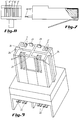
- FIG. 1 there is illustrated a female connector according to the invention.
- This connector comprises a first pair of connection pins 1 located in a first holder part 7 and a second pair of connection pins 2 located in a second holder part 8.
- a further holder part 9 is designed for receiving an RJ-45 male connector as will be described further.
- This further holder part comprises a series of connection pins 3 to 6, comprising at a first extremity of the series a third pair of connection pins 3 and at the other extremity a fourth pair of connection pins 4.
- a series of eight wires 10-17 are provided for being connected to the connection pins 1 to 4 respectively.
- the pairs of wires are separated from one another in order to reduce crosstalk at their connection with the connection pins.
- each pair of wires is shielded, as illustrated in Figure 2.
- connection pins there are provided a central pair 5 and a further pair 6 of connection pins, so as to mate with the corresponding pins provided in a standard RJ-45 male connector, as will be described further when referring to Figures 7 and 8.
- Figure 5 illustrates that the further pair 6 of connection pins from the female connector is electrically connected to the second pair 2 of connection pins, by means of electrical connections 18. Similarly the central pair 5 of connection pins is electrically connected to the first pair 1 of connection pins (not shown).
- the electrical connections 18 are released, so that signals transmitted through wires 14' to 17' will be transmitted to the wires 14 to 17 through the intermediary of pins 1'-1 and 2'-2 and will not pass through the pins 5 and 6.
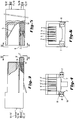
- the holder part 8' from the male connector comprises a shield 19 ( Figures 3-4) in such a manner that upon plugging in this connector in the female connector ( Figures 5-6), the further pair 6 of pins may be grounded since the released electrical connection 18 comes into contact with the shield 19.
- the holder part 7' could for the same reason also be shielded so as to ground the central pair 5 of pins.
- the central pair is not grounded but used for an additional signal.
- the male connector comprises a corresponding central pair 5' of pins.
- the male connector may also comprise a further pair 6' of pins.
- the first 1' and second 2' pairs of pins are not connected to the central 5' and further 6' pairs of pins.
- Figures 7 and 8 illustrate a standard RJ-45 male connector.
- the first 1 and second 2 pairs of pins are not connected to corresponding pins of the male connector.
- wires 14 to 17 which are connected to those pins 1 and 2.
- the electrical connections 18 guarantee the transmission of signals from the corresponding wires 14'' to 17'' from the male connector ( Figure 7) to the wires 14 to 17 from the female connector, since the signals are transmitted from the central 5 and further 6 pairs of pins to the first 1 and second 2 pairs of pins and follow the path 5''-5-1-14&15 and 6''-6-2-16&17.
- central and further pairs of pins may be omitted from the male connector of Figures 3 and 4, or may be used according to an alternative for additional signals.
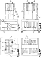
- the male connector according to Figure 9 comprises also the first 1', second 2', third 3' and fourth 4' pair of pins as described before.
- each pair of pins is provided in a corresponding holder part.
- the shield 20 is provided for grounding the further pair of pins 6 of the female connector (see Figure 15) upon connection of the male connector. This may for example be achieved by providing a connection plate 21 connecting the shield 20 with the pins 6.
- the central pair of pins 5 is also grounded.
- the shield makes only contact with the further pair of pins so that the central pair of pins may be used for an additional electrical signal.
- the male ( Figure 12) and female ( Figure 17) connectors further comprise connection forks 22 provided for readily connecting the wires of the cable (not shown).
- the second connection pins 2 are separated into two portions 2a and 2b.
- the first connection pins 1 are separated into two portions (not shown).
- the central pair of pins 5 is connected to a first electrical contact (not shown) connecting the central pair of pins with the first pair of pins 1.
- each pin of the further pair of pins 6 is connected to a second electrical contact 26 connecting the further pair of pins 6 with the second portion 2b of the second pair of pins.
- protrusion 23 provided on the male connector will release the contact between the second electrical contact 26 from the second portion 2b of the second connection pins and connect at the same time the first portion 2a with the second portion 2b from the second pair of pins so that electrical signals from the wires connected to the second pair of pins 2' of the male connector are transmitted to the corresponding wires connected to the second pair of pins 2 of the female connector.
- protrusion 23 will release the contact between the first electrical contact (not shown) from the second portion of the first connection pins and connect at the same time the first portion with the second portion from the first pair of pins 1 so that electrical signals from the wires connected to the first pair of pins 1' of the male connector are transmitted to the corresponding wires connected to the first pair of pins 1 of the female connector.
- the male connector according to Figures 9 to 13 comprises a protuberance 24 and the female connector comprises corresponding notches 25 (as illustrated in Figure15), in order to prevent the connection of the male connector according to the invention in a conventional female RJ-45 connector. Connection of a conventional RJ-45 male connector to the female connector according to the invention is still enabled.
- the first electrical contact connecting the central pair of pins with the first pair of pins will be held, so that electrical signals from the wires connected to the central pair of pins of the conventional male connector are transmitted to the wires connected to the first pair of pins 1 of the female connector.
- the second electrical contact 26 connecting the further pair of pins 6 with the second pair of pins 2b will be held, so that electrical signals from the wires connected to the central pair of pins of the conventional male connector are transmitted to the wires connected to the second pair of pins 2b of the female connector.
Landscapes
- Details Of Connecting Devices For Male And Female Coupling (AREA)
- Coupling Device And Connection With Printed Circuit (AREA)
Priority Applications (5)
| Application Number | Priority Date | Filing Date | Title |
|---|---|---|---|
| DE69808595T DE69808595T2 (de) | 1998-02-04 | 1998-02-04 | Kontaktsatz |
| EP98400233A EP0940890B1 (de) | 1998-02-04 | 1998-02-04 | Kontaktsatz |
| JP02546499A JP4312866B2 (ja) | 1998-02-04 | 1999-02-02 | コンタクトセット |
| CN99101861A CN1108008C (zh) | 1998-02-04 | 1999-02-03 | 触点组 |
| US09/243,453 US6193533B1 (en) | 1998-02-04 | 1999-02-03 | Contact set |
Applications Claiming Priority (1)
| Application Number | Priority Date | Filing Date | Title |
|---|---|---|---|
| EP98400233A EP0940890B1 (de) | 1998-02-04 | 1998-02-04 | Kontaktsatz |
Publications (2)
| Publication Number | Publication Date |
|---|---|
| EP0940890A1 true EP0940890A1 (de) | 1999-09-08 |
| EP0940890B1 EP0940890B1 (de) | 2002-10-09 |
Family
ID=8235259
Family Applications (1)
| Application Number | Title | Priority Date | Filing Date |
|---|---|---|---|
| EP98400233A Expired - Lifetime EP0940890B1 (de) | 1998-02-04 | 1998-02-04 | Kontaktsatz |
Country Status (5)
| Country | Link |
|---|---|
| US (1) | US6193533B1 (de) |
| EP (1) | EP0940890B1 (de) |
| JP (1) | JP4312866B2 (de) |
| CN (1) | CN1108008C (de) |
| DE (1) | DE69808595T2 (de) |
Cited By (7)
| Publication number | Priority date | Publication date | Assignee | Title |
|---|---|---|---|---|
| DE10053843C1 (de) * | 2000-10-30 | 2002-06-20 | Siemens Ag | Ethernet Steckverbindung mit zusätzlichen Kontakten zur Spannungsversorgungseinspeisung |
| DE10065595A1 (de) * | 2000-12-28 | 2002-08-14 | Ackermann Albert Gmbh Co | Elektrisches Steckverbindersystem sowie Stecker und Buchse für Steckverbindersystem |
| EP2096715A3 (de) * | 2008-02-27 | 2011-01-05 | Olympus Medical Systems Corp. | Elektrischer Steckverbinder |
| WO2011025525A1 (en) * | 2009-08-25 | 2011-03-03 | Tyco Electronics Corporation | Electrical connector with separable contacts |
| US8016621B2 (en) | 2009-08-25 | 2011-09-13 | Tyco Electronics Corporation | Electrical connector having an electrically parallel compensation region |
| US8128436B2 (en) | 2009-08-25 | 2012-03-06 | Tyco Electronics Corporation | Electrical connectors with crosstalk compensation |
| US8435082B2 (en) | 2010-08-03 | 2013-05-07 | Tyco Electronics Corporation | Electrical connectors and printed circuits having broadside-coupling regions |
Families Citing this family (14)
| Publication number | Priority date | Publication date | Assignee | Title |
|---|---|---|---|---|
| USD461449S1 (en) | 2000-11-16 | 2002-08-13 | J.S.T. Mfg., Ltd. | Connector for printed circuit boards |
| USD461769S1 (en) | 2000-11-16 | 2002-08-20 | J.S.T. Mfg., Ltd. | Connector for printed circuit boards |
| US6554366B2 (en) * | 2001-09-14 | 2003-04-29 | L & P Property Management Company | Nut plate retainer |
| US8182294B2 (en) | 2007-05-07 | 2012-05-22 | Ortronics, Inc. | Connector assembly and related methods of use |
| US8758047B2 (en) | 2007-05-07 | 2014-06-24 | Ortronics, Inc. | Port replication assembly with adapter cable and related methods of use |
| US7601024B2 (en) * | 2007-05-07 | 2009-10-13 | Ortronics, Inc. | Shielded connector assembly for preterminated systems |
| US7628657B2 (en) | 2007-05-07 | 2009-12-08 | Ortronics, Inc. | Connector assembly for use with plugs and preterminated cables |
| US7485010B2 (en) * | 2007-06-14 | 2009-02-03 | Ortronics, Inc. | Modular connector exhibiting quad reactance balance functionality |
| US7481678B2 (en) * | 2007-06-14 | 2009-01-27 | Ortronics, Inc. | Modular insert and jack including bi-sectional lead frames |
| US9455765B2 (en) | 2011-09-07 | 2016-09-27 | Commscope, Inc. Of North Carolina | Communications connectors having frequency dependent communications paths and related methods |
| US9112320B2 (en) | 2012-02-23 | 2015-08-18 | Commscope, Inc. Of North Carolina | Communications connectors having electrically parallel sets of contacts |
| US9246285B2 (en) | 2013-03-13 | 2016-01-26 | Panduit Corp. | Network jack with backwards capability and systems using same |
| US9419391B2 (en) | 2013-08-20 | 2016-08-16 | Panduit Corp. | Communication connector |
| US10559927B2 (en) | 2013-10-11 | 2020-02-11 | Panduit Corp. | Switchable RJ45/ARJ45 jack |
Citations (5)
| Publication number | Priority date | Publication date | Assignee | Title |
|---|---|---|---|---|
| US4261633A (en) * | 1979-08-27 | 1981-04-14 | Amp Incorporated | Wiring module for telephone jack |
| US4682837A (en) * | 1984-07-26 | 1987-07-28 | The Siemon Company | Eight conductor modular plug |
| EP0692884A1 (de) * | 1994-07-14 | 1996-01-17 | Molex Incorporated | Modularer Steckverbinder mit verringertem Übersprechen |
| EP0755100A2 (de) * | 1996-02-29 | 1997-01-22 | Telesafe AS | Kontaktsatz für Kabel mit verdrillten, einzeln abgeschirmten Leitungspaaren |
| WO1997041624A1 (en) * | 1996-04-26 | 1997-11-06 | Austin Taylor Communications Limited | Electrical socket for two plugs |
Family Cites Families (9)
| Publication number | Priority date | Publication date | Assignee | Title |
|---|---|---|---|---|
| US4717217A (en) * | 1980-02-12 | 1988-01-05 | Virginia Patent Development Corporation | Connector for mating modular plug with printed circuit board |
| US4699443A (en) * | 1984-12-28 | 1987-10-13 | American Telephone And Telegraph Company | Modular telephone jack |
| US4682827A (en) | 1985-08-26 | 1987-07-28 | Woodward Eldon D | Combination toy box-drafting table |
| GB8600831D0 (en) * | 1986-01-15 | 1986-02-19 | Amp Italia | Modular jack |
| US5030123A (en) * | 1989-03-24 | 1991-07-09 | Adc Telecommunications, Inc. | Connector and patch panel for digital video and data |
| US5123854A (en) * | 1991-03-13 | 1992-06-23 | Molex Incorporated | Shunted electrical connector |
| US5961354A (en) * | 1997-01-13 | 1999-10-05 | Lucent Technologies, Inc. | Electrical connector assembly |
| US5921818A (en) * | 1997-06-23 | 1999-07-13 | Lucent Technologies Inc. | Low crosstalk electrical connector |
| US5951330A (en) * | 1997-09-03 | 1999-09-14 | Lucent Technologies Inc. | Alignment apparatus for use in the jack interface housing of a communication plug |
-
1998
- 1998-02-04 EP EP98400233A patent/EP0940890B1/de not_active Expired - Lifetime
- 1998-02-04 DE DE69808595T patent/DE69808595T2/de not_active Expired - Lifetime
-
1999
- 1999-02-02 JP JP02546499A patent/JP4312866B2/ja not_active Expired - Fee Related
- 1999-02-03 US US09/243,453 patent/US6193533B1/en not_active Expired - Lifetime
- 1999-02-03 CN CN99101861A patent/CN1108008C/zh not_active Expired - Fee Related
Patent Citations (5)
| Publication number | Priority date | Publication date | Assignee | Title |
|---|---|---|---|---|
| US4261633A (en) * | 1979-08-27 | 1981-04-14 | Amp Incorporated | Wiring module for telephone jack |
| US4682837A (en) * | 1984-07-26 | 1987-07-28 | The Siemon Company | Eight conductor modular plug |
| EP0692884A1 (de) * | 1994-07-14 | 1996-01-17 | Molex Incorporated | Modularer Steckverbinder mit verringertem Übersprechen |
| EP0755100A2 (de) * | 1996-02-29 | 1997-01-22 | Telesafe AS | Kontaktsatz für Kabel mit verdrillten, einzeln abgeschirmten Leitungspaaren |
| WO1997041624A1 (en) * | 1996-04-26 | 1997-11-06 | Austin Taylor Communications Limited | Electrical socket for two plugs |
Cited By (19)
| Publication number | Priority date | Publication date | Assignee | Title |
|---|---|---|---|---|
| DE10053843C1 (de) * | 2000-10-30 | 2002-06-20 | Siemens Ag | Ethernet Steckverbindung mit zusätzlichen Kontakten zur Spannungsversorgungseinspeisung |
| DE10065595A1 (de) * | 2000-12-28 | 2002-08-14 | Ackermann Albert Gmbh Co | Elektrisches Steckverbindersystem sowie Stecker und Buchse für Steckverbindersystem |
| EP1220375A3 (de) * | 2000-12-28 | 2003-06-11 | Albert Ackermann GmbH & Co. KG | Elektrisches Steckverbindersystem sowie Stecker und Buchse für Steckverbindersystem |
| EP2096715A3 (de) * | 2008-02-27 | 2011-01-05 | Olympus Medical Systems Corp. | Elektrischer Steckverbinder |
| US8282425B2 (en) | 2009-08-25 | 2012-10-09 | Tyco Electronics Corporation | Electrical connectors having open-ended conductors |
| US8496501B2 (en) | 2009-08-25 | 2013-07-30 | Tyco Electronics Corporation | Electrical connector with separable contacts |
| US8016621B2 (en) | 2009-08-25 | 2011-09-13 | Tyco Electronics Corporation | Electrical connector having an electrically parallel compensation region |
| US8128436B2 (en) | 2009-08-25 | 2012-03-06 | Tyco Electronics Corporation | Electrical connectors with crosstalk compensation |
| WO2011025525A1 (en) * | 2009-08-25 | 2011-03-03 | Tyco Electronics Corporation | Electrical connector with separable contacts |
| US8287316B2 (en) | 2009-08-25 | 2012-10-16 | Tyco Electronics Corporation | Electrical connector with separable contacts |
| US9787015B2 (en) | 2009-08-25 | 2017-10-10 | Commscope Technologies Llc | Electrical connector with separable contacts |
| US7967644B2 (en) | 2009-08-25 | 2011-06-28 | Tyco Electronics Corporation | Electrical connector with separable contacts |
| US8632368B2 (en) | 2009-08-25 | 2014-01-21 | Tyco Electronics Corporation | Electrical connector with separable contacts |
| US9124043B2 (en) | 2009-08-25 | 2015-09-01 | Tyco Electronics Corporation | Electrical connectors having open-ended conductors |
| US9198289B2 (en) | 2009-08-25 | 2015-11-24 | Tyco Electronics Services Gmbh | Electrical connectors and printed circuits having broadside-coupling regions |
| US9660385B2 (en) | 2009-08-25 | 2017-05-23 | Commscope Technologies Llc | Electrical connectors having open-ended conductors |
| US9692180B2 (en) | 2009-08-25 | 2017-06-27 | Commscope Technologies Llc | Electrical connectors and printed circuits having broadside-coupling regions |
| US8435082B2 (en) | 2010-08-03 | 2013-05-07 | Tyco Electronics Corporation | Electrical connectors and printed circuits having broadside-coupling regions |
| US10135194B2 (en) | 2010-08-03 | 2018-11-20 | Commscope Technologies Llc | Electrical connectors and printed circuits having broadside-coupling regions |
Also Published As
| Publication number | Publication date |
|---|---|
| CN1243346A (zh) | 2000-02-02 |
| JP4312866B2 (ja) | 2009-08-12 |
| CN1108008C (zh) | 2003-05-07 |
| JP2000113944A (ja) | 2000-04-21 |
| DE69808595D1 (de) | 2002-11-14 |
| EP0940890B1 (de) | 2002-10-09 |
| US6193533B1 (en) | 2001-02-27 |
| DE69808595T2 (de) | 2003-06-18 |
Similar Documents
| Publication | Publication Date | Title |
|---|---|---|
| EP0940890B1 (de) | Kontaktsatz | |
| US11811168B2 (en) | Connector assembly | |
| JP4318810B2 (ja) | 漏話が低減されると共に異なる接触装置で使用されるように構成されたモジュラコネクタ | |
| EP0426348B1 (de) | Kabelverbinder mit niedriger Induktanzbahn | |
| EP0646996B1 (de) | Blindsteck-Führung mit Erdungskontakt | |
| EP1274151B1 (de) | USB elektrischer Verbinder | |
| CA2262727C (en) | Low crosstalk connector configuration | |
| EP1168525B1 (de) | Für die Verarbeitung von verschiedenen Signalarten inklusive Signale mit hoher Geschwindigkeit verwendbarer Verbinder | |
| US5639266A (en) | High frequency electrical connector | |
| US6739904B2 (en) | Cable connector assembly | |
| US4341428A (en) | Interconnection system for shielded electrical cable | |
| US9692181B2 (en) | Matched high-speed interconnector assembly | |
| US5267868A (en) | Shielded electrical connector assemblies | |
| EP0486298A1 (de) | Mehrpoliger Verbinder zur Signalübertragung | |
| US20040077222A1 (en) | High performance jack for telecommunication applications | |
| EP0755100B1 (de) | Kontaktsatz für Kabel mit verdrillten, einzeln abgeschirmten Leitungspaaren | |
| US6176743B1 (en) | Electrical adapter | |
| EP2939314B1 (de) | Schnittstellenadapter | |
| US5340333A (en) | Shielded modular adapter | |
| JPH11224741A (ja) | モジュラープラグ | |
| MX2008011542A (es) | Receptaculo con arreglo de contacto para optimizacion de interferencia. | |
| US7645168B2 (en) | Distribution module for converting between symmetrical and asymmetrical data transmission paths | |
| US6869321B1 (en) | Dual female electrical connector and connector module | |
| US7066769B2 (en) | Electrical connector | |
| EP0393670A2 (de) | Sich selbst abschliessender Steckverbinder und Kabelanordnung |
Legal Events
| Date | Code | Title | Description |
|---|---|---|---|
| PUAI | Public reference made under article 153(3) epc to a published international application that has entered the european phase |
Free format text: ORIGINAL CODE: 0009012 |
|
| AK | Designated contracting states |
Kind code of ref document: A1 Designated state(s): BE CH DE FR GB IT LI |
|
| AX | Request for extension of the european patent |
Free format text: AL;LT;LV;MK;RO;SI |
|
| 17P | Request for examination filed |
Effective date: 20000308 |
|
| AKX | Designation fees paid |
Free format text: BE CH DE FR GB IT LI |
|
| RAP1 | Party data changed (applicant data changed or rights of an application transferred) |
Owner name: NEXANS |
|
| 17Q | First examination report despatched |
Effective date: 20011017 |
|
| GRAG | Despatch of communication of intention to grant |
Free format text: ORIGINAL CODE: EPIDOS AGRA |
|
| RIC1 | Information provided on ipc code assigned before grant |
Free format text: 7H 01R 24/00 A, 7H 01R 27/00 B, 7H 01R 12/16 B |
|
| GRAG | Despatch of communication of intention to grant |
Free format text: ORIGINAL CODE: EPIDOS AGRA |
|
| GRAH | Despatch of communication of intention to grant a patent |
Free format text: ORIGINAL CODE: EPIDOS IGRA |
|
| RIC1 | Information provided on ipc code assigned before grant |
Free format text: 7H 01R 24/00 A, 7H 01R 27/00 B, 7H 01R 12/16 B |
|
| GRAH | Despatch of communication of intention to grant a patent |
Free format text: ORIGINAL CODE: EPIDOS IGRA |
|
| GRAA | (expected) grant |
Free format text: ORIGINAL CODE: 0009210 |
|
| AK | Designated contracting states |
Kind code of ref document: B1 Designated state(s): BE CH DE FR GB IT LI |
|
| REG | Reference to a national code |
Ref country code: GB Ref legal event code: FG4D |
|
| REG | Reference to a national code |
Ref country code: CH Ref legal event code: EP |
|
| REF | Corresponds to: |
Ref document number: 69808595 Country of ref document: DE Date of ref document: 20021114 |
|
| REG | Reference to a national code |
Ref country code: CH Ref legal event code: NV Representative=s name: CRONIN INTELLECTUAL PROPERTY |
|
| ET | Fr: translation filed | ||
| PLBE | No opposition filed within time limit |
Free format text: ORIGINAL CODE: 0009261 |
|
| STAA | Information on the status of an ep patent application or granted ep patent |
Free format text: STATUS: NO OPPOSITION FILED WITHIN TIME LIMIT |
|
| 26N | No opposition filed |
Effective date: 20030710 |
|
| REG | Reference to a national code |
Ref country code: CH Ref legal event code: PCAR Free format text: CRONIN INTELLECTUAL PROPERTY;CHEMIN DE PRECOSSY 31;1260 NYON (CH) |
|
| REG | Reference to a national code |
Ref country code: FR Ref legal event code: PLFP Year of fee payment: 19 |
|
| PGFP | Annual fee paid to national office [announced via postgrant information from national office to epo] |
Ref country code: CH Payment date: 20160217 Year of fee payment: 19 Ref country code: DE Payment date: 20160218 Year of fee payment: 19 Ref country code: IT Payment date: 20160223 Year of fee payment: 19 |
|
| PGFP | Annual fee paid to national office [announced via postgrant information from national office to epo] |
Ref country code: FR Payment date: 20160218 Year of fee payment: 19 Ref country code: BE Payment date: 20160217 Year of fee payment: 19 Ref country code: GB Payment date: 20160217 Year of fee payment: 19 |
|
| PG25 | Lapsed in a contracting state [announced via postgrant information from national office to epo] |
Ref country code: BE Free format text: LAPSE BECAUSE OF NON-PAYMENT OF DUE FEES Effective date: 20170228 |
|
| REG | Reference to a national code |
Ref country code: DE Ref legal event code: R119 Ref document number: 69808595 Country of ref document: DE |
|
| REG | Reference to a national code |
Ref country code: CH Ref legal event code: PL |
|
| GBPC | Gb: european patent ceased through non-payment of renewal fee |
Effective date: 20170204 |
|
| PG25 | Lapsed in a contracting state [announced via postgrant information from national office to epo] |
Ref country code: CH Free format text: LAPSE BECAUSE OF NON-PAYMENT OF DUE FEES Effective date: 20170228 Ref country code: LI Free format text: LAPSE BECAUSE OF NON-PAYMENT OF DUE FEES Effective date: 20170228 |
|
| REG | Reference to a national code |
Ref country code: FR Ref legal event code: ST Effective date: 20171031 |
|
| PG25 | Lapsed in a contracting state [announced via postgrant information from national office to epo] |
Ref country code: DE Free format text: LAPSE BECAUSE OF NON-PAYMENT OF DUE FEES Effective date: 20170901 Ref country code: FR Free format text: LAPSE BECAUSE OF NON-PAYMENT OF DUE FEES Effective date: 20170228 |
|
| REG | Reference to a national code |
Ref country code: BE Ref legal event code: MM Effective date: 20170228 |
|
| PG25 | Lapsed in a contracting state [announced via postgrant information from national office to epo] |
Ref country code: IT Free format text: LAPSE BECAUSE OF NON-PAYMENT OF DUE FEES Effective date: 20170204 Ref country code: GB Free format text: LAPSE BECAUSE OF NON-PAYMENT OF DUE FEES Effective date: 20170204 |