EP0940973A2 - Appareil de régistration et procédé d'imagerie à résolution variable - Google Patents
Appareil de régistration et procédé d'imagerie à résolution variable Download PDFInfo
- Publication number
- EP0940973A2 EP0940973A2 EP99200470A EP99200470A EP0940973A2 EP 0940973 A2 EP0940973 A2 EP 0940973A2 EP 99200470 A EP99200470 A EP 99200470A EP 99200470 A EP99200470 A EP 99200470A EP 0940973 A2 EP0940973 A2 EP 0940973A2
- Authority
- EP
- European Patent Office
- Prior art keywords
- transfer gate
- green
- photosensor
- red
- blue
- Prior art date
- Legal status (The legal status is an assumption and is not a legal conclusion. Google has not performed a legal analysis and makes no representation as to the accuracy of the status listed.)
- Withdrawn
Links
- 238000000034 method Methods 0.000 title claims abstract description 14
- 238000003384 imaging method Methods 0.000 title abstract description 34
- 238000012546 transfer Methods 0.000 claims abstract description 171
- 230000003287 optical effect Effects 0.000 claims abstract description 151
- 238000003491 array Methods 0.000 claims abstract description 42
- 230000003111 delayed effect Effects 0.000 claims description 9
- 230000033001 locomotion Effects 0.000 claims description 7
- 230000000737 periodic effect Effects 0.000 abstract description 6
- 230000001960 triggered effect Effects 0.000 abstract description 5
- 230000004044 response Effects 0.000 abstract description 3
- 238000001444 catalytic combustion detection Methods 0.000 description 9
- 230000010354 integration Effects 0.000 description 7
- 230000006870 function Effects 0.000 description 5
- 238000005286 illumination Methods 0.000 description 5
- 230000010363 phase shift Effects 0.000 description 5
- 238000012805 post-processing Methods 0.000 description 5
- 238000000926 separation method Methods 0.000 description 5
- 238000012545 processing Methods 0.000 description 4
- 230000005855 radiation Effects 0.000 description 4
- 238000012937 correction Methods 0.000 description 3
- 238000012986 modification Methods 0.000 description 3
- 230000004048 modification Effects 0.000 description 3
- 238000005070 sampling Methods 0.000 description 3
- 238000011982 device technology Methods 0.000 description 2
- 238000010586 diagram Methods 0.000 description 2
- 238000001914 filtration Methods 0.000 description 2
- 239000011521 glass Substances 0.000 description 2
- 230000005484 gravity Effects 0.000 description 2
- 230000007246 mechanism Effects 0.000 description 2
- 230000003595 spectral effect Effects 0.000 description 2
- 239000000758 substrate Substances 0.000 description 2
- 238000012952 Resampling Methods 0.000 description 1
- 230000005540 biological transmission Effects 0.000 description 1
- 238000006243 chemical reaction Methods 0.000 description 1
- 230000000593 degrading effect Effects 0.000 description 1
- 230000001934 delay Effects 0.000 description 1
- 238000012634 optical imaging Methods 0.000 description 1
- 230000005693 optoelectronics Effects 0.000 description 1
- 230000037361 pathway Effects 0.000 description 1
- 230000008569 process Effects 0.000 description 1
- 230000006335 response to radiation Effects 0.000 description 1
- 230000035945 sensitivity Effects 0.000 description 1
- 239000007787 solid Substances 0.000 description 1
Images










Classifications
-
- H—ELECTRICITY
- H04—ELECTRIC COMMUNICATION TECHNIQUE
- H04N—PICTORIAL COMMUNICATION, e.g. TELEVISION
- H04N1/00—Scanning, transmission or reproduction of documents or the like, e.g. facsimile transmission; Details thereof
- H04N1/46—Colour picture communication systems
- H04N1/48—Picture signal generators
- H04N1/486—Picture signal generators with separate detectors, each detector being used for one specific colour component
Definitions
- the field of the present invention relates to high resolution color and monochromatic imaging capturing systems including digital imaging systems, which employ a Charged Coupled Device, (CCD).
- CCD Charged Coupled Device
- the field of the present invention relates to the scanning or capturing of high-resolution images including color and monochromatic images using image scanners, digital cameras, facsimile machines, photocopiers, or other image capturing systems and methods, and the like.
- An original image is the actual information content, displayed on a document, or the like, which is to be captured.
- an original image may include text, line art, color or monochrome photographic or halftone images, graphics, artwork or the like, alone or in combination.
- a sensing system for capturing an original image comprises one or more radiation sensitive elements for providing an electrical signal in response to radiation falling thereon.
- CCD Charged Coupled Device
- a CCD array comprises a plurality of individual pixels, each addressable to determine a voltage value generated by an amount of radiation falling on an individual pixel and wherein the plurality of pixels may be arranged in a single linear row or in a two dimensional array.
- a tri-linear CCD comprises three linear arrays of individually addressable pixels, each arranged for capturing an image of a different portion of the original image and each including a color mask positioned between the array of pixels and the original image such that only light of a color transmitted by the color mask exposes the individual pixels of the array.
- each of the three linear arrays of pixels may be moved or scanned across an original image such that e.g. a first array captures only a red portion of the original image, a second array captures only a green portion of the original image and a third array captures only a blue portion of the original image when a red, green and blue filter set are used.
- the Linetime, T, or integration time is the amount of time required to integrate the voltage signal of a CCD pixel, or linear array of CCD pixels, in order to achieve an appropriate electrical signal representative of the level of radiation falling onto the pixel or array of pixels.
- the linetime usually depends on the illumination level of the original image an is usually constant for a given scanning system.
- the linear array will move over a portion of the original image during the linetime duration.
- the portion of the original image traversed by the linear array during one linetime is defined as a scan line.
- the linetime starts at t N-1 and ends at t N when the CCD array has moved to line N+1.
- the linetime is substantially equal to the time between two consecutive transfer gate pulses, i.e. the pulse which transfers the voltage accumulated in CCD array during the linetime.
- the period of the transfer gate pulse signal is given by T.
- a pixel may be defined as a single element of a CCD array or the portion of the original image captured by a single element of a CCD during the linetime.
- the resolution of a scan or image refers how many pixels are sampled per unit of distance.
- an x-direction which is defined as parallel to a longitudinal axis of a linear CCD array axis or parallel to a scan line, the resolution is defined by the pitch of individual CCD elements.
- a y-direction which is defined as the direction of relative motion between the linear CCD array and the original image, the resolution is determined by the speed of the relative motion of the array over the original image.
- the optical resolution, or base resolution is the y-resolution, (and therefore speed of the relative motion of the linear array over the original image), which corresponds to the pitch of the CCD elements in the x-direction.
- the captured pixels are square.
- Resolution [dpi] 25.4[mm/in] (speed[mm/sec]) (linetime[sec])
- Resolution [ppmm] 1 (speed[mm/sec]) (linetime[sec]) (Where “dpi” is dots per inch, “mm” is millimeters, “ppmm” is pixels per millimeter, “in” is inches, and, “sec” is seconds.)
- optical imaging system employs a magnification ratio of one an original image pixel at optical resolution is equal to the size of the CCD element. At other resolutions or scan speeds, and other magnification ratios original image pixel sizes will typically be larger.
- an original image may be scanned at a number of resolutions in the y-direction by changing the speed of movement of the linear array with respect to the original image.
- the size of a pixel scanned at a resolution other than the optical resolution is proportional to the optical resolution divided by the scanning resolution. For example, if a scanning system has an optical resolution of 4,000 dpi (i.e. the CCD elements have a pitch of 10 ⁇ m in the x-direction), and it is desired to scan the original at 1600 dpi the scanned or sampled pixel size in the y-direction is 2.5 times larger or approximately having a pitch of 25 ⁇ m.
- BGR - blue, green and red also used in reference with the three primary color separations of the CCD.
- TRANSFER GATE SIGNAL, TG(t) is a periodic timing signal generated by any known microprocessor, oscillator, timing or clock means to trigger a CCD photosensor array.
- TRANSFER GATE RECEIVING MEANS are the pin-outs on the photosensor array, e.g., a CCD, for receiving the Transfer Gate Signal(s); the channels for receiving trigger signals and the like.
- OPTICAL LINE SPACING OLS(K+1:K)
- OLS(K+1:K) is the interchannel spacing, i.e., the distance, center to center, leading edge to leading edge, or trailing edge to trailing edge between a leading photosensor array K and a lagging photosensor K+1.
- the spacing between the color channels In particular in a tri-linear CCD array the spacing between the color channels.
- the optical line or interchannel spacing is specified in units of micrometers, pixels or number of scan lines at optical resolution.
- the optical line spacing between the red and green sensors will be referenced with the notation OLS(R:G).
- the green-blue optical line spacing will be referenced with OLS(G:B) and the red-blue optical line spacing with OLS(R:B).
- OLS(K+1:K) the optical line spacing, between a lagging K+1 and leading K photosensor array, respectively, may be hereinafter referred to as, OLS(K+1:K), where K+1 and K are lagging and leading sensors, respectively.
- LINESKIP is the number of scan lines between the R, G and B channels of a tri-linear CCD array.
- the lineskip is simply the interchannel or optical line spacing between the R, G, B channels.
- notation may be used in referring to the LINESKIP between a given pair of photosensors.
- LINESKIP(R:G) may be used to represent the lineskip between the red and green color photosensors.
- the lineskip between a lagging photosensor array K+1 and a leading photosensor array K, respectively may be hereinafter referred to as, LINESKIP(K+1:K), where K and K+1 are leading and lagging sensors, respectively.
- FRACTIONAL LINESKIP for example, in color scanning systems utilizing a trilinear CCD, a FRACTIONAL LINESKIP occurs at resolutions in which the LINESKIP, the optical line spacing between a pair of color sensors divided by the scanned pixel size, is not equal to an integer.
- FRAC(x) may hereinafter be used on occasion to abbreviate FRACTIONAL(x).
- an original image on a substrate is illuminated along a scan line and the illumination energy reflected from, or transmitted through the substrate is captured by an optical system to form an image of the scan line on a sensor, such as a tri-linear CCD array.
- the sensor, or CCD converts the optical image of the scan to an electronic signal representation of the scan line.
- a desired portion of the original is scanned by simultaneously moving the illumination system, optical system and CCD sensor relative to the original along a motion direction hereinafter referred to as the "scanning or y-direction.
- systems also exist in which the original document is moved relative to a fixed optical system.
- a tri-linear CCD is comprised of three rows or channels of photosensor elements, for capturing a red, green and a blue component of the original image.
- the spacing between the color channels or interchannel spacing may be specified in units of microns, pixels or number of scan lines at optical resolution and is preferably equal to an integer number of pixel lengths or optical line spacings (OLS).
- OLS optical line spacings
- CCD part number KLI-8013 manufactured by the EASTMAN KODAK Company has blue, green and red sensor arrays spaced equally apart in the scanning direction by a distance of 108 ⁇ m or 12 9 micron pixels.
- CCDs of the prior art have one common transfer gate receiving means for transferring voltages from each of the three color channels so that all three color sensors are activated to scan simultaneously.
- each channel is scanning a different portion of the original image or different scan line.
- the separation between the channels measured in scan lines depends on the scanning resolution in the y-direction. Since at optical resolution the inter-channel spacing between the color channels is equal to a integer number of scan lines, the data from a scan line scanned by the leading channel e.g. the blue channel of Figure 5 is easily matched up with the data provided by the trailing red and green channels when these channels scan the same scan line at a later time.
- the present invention solves the problems of the prior art without increasing memory requirements and without extensive post processing and filtering of raw shifted pixel data.
- the need for time consuming multi-pass scanning or imaging is eliminated.
- the teachings of the present invention reduce the need for CCDs with expensive precision made optical line spacings.
- the photo to electronic conversion is performed by a sensing system employing a plurality of photosensor arrays such as a CCD, having an independent transfer gate receiving means for each photosensor.
- the sensing system which employs a plurality of photosensor arrays such as a CCD, does not need to have an optical line spacing between sensor arrays (the interchannel spacing) equivalent to an integer number of optical pixel lengths.
- a method for registering a plurality of fractionally shifted integrated scenes for an imaging system comprising an optical system and a sensing system, said sensing system including an integer number of photosensor arrays wherein said integer is a number N greater than or equal to 2, said photosensor arrays having optical line spacings OLS(K+1:K) in reference to a leading photosensor array K and with respect to a lagging photosensor array K+1, for K equal to an integer from 1 to N-1, and wherein each of said plurality of N photosensor arrays further includes corresponding N transfer gate receiving means so that each of said N photosensor arrays is capable of being independently triggered to pass accumulated charge in the photo site into electrical signals in response to a corresponding one of a plurality of transfer gate signals, TG i (t), where i is an integer from 1 to N and wherein each one of said transfer gate signals has a periodicity T and angular frequency ⁇ , said transfer gate signals being of the general form TG i (
- the number of N photosensor arrays comprises three photosensor arrays, a blue photosensor array, a green photosensor array and a red photosensor array for blue, green and red color spectral separation, respectively, said blue, green and red photosensor arrays further including a blue, green and red transfer gate receiving means, respectively.
- a blue transfer gate signal TG B ( ⁇ t) corresponds to said blue transfer gate receiving means for said blue photosensor array
- a green transfer gate signal TG G ( ⁇ t) corresponds to said green transfer gate receiving means for said green photosensor array
- a red transfer gate signal TG R ( ⁇ t) corresponds to said red transfer gate receiving means for said red photosensor array
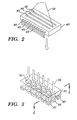
- FIGS. 1-3 illustrate the interrelationships between components including a CCD of a typical imaging device such as a flat bed scanner.
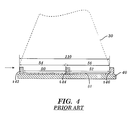
- FIG. 4 is a sectioned view taken along 4-4 of FIG. 3 and a diagrammatic representation of the inner components of the CCD viewed on edge in the scanning direction, or moving direction, of the CCD.
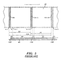
- FIG. 5 illustrates how an image is scanned in real time at an optical resolution utilizing a common transfer gate system.
- FIG. 6A is a perspective view of FIG. 5 taken along the y-axis illustrating the integrated scenes for each color, BGR, which align left justified as a result of an optical resolution scan.
- FIG. 6B is an edge-view diagram of FIG. 6A taken along the y-axis illustrating the integrated scenes for each color, BGR, which align left justified as a result of an optical resolution scan.
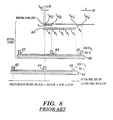
- FIGS. 7-9 illustrate the general misregistration errors which occur when the lineskip has a fractional component, the fractional lineskip, for resolutions in which the optical line spacing divided by the sampled pixel size is not equal to an integer.
- FIG. 10 is an edge-view diagram taken along the y-axis illustrating the integrated scenes for each color, BGR, which misregister and do not align left justified when a scan is performed at resolution in which the lineskip has a fractional component, (fractional lineskip).
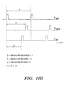
- FIGS. 11A-B show how the transfer gate signals for the present invention are related through phase shifts with respect to time.
- FIGS. 12A-B compare an imaging system of the prior art with the imaging system and method of the present invention.
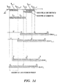
- FIGS. 13-14 show how the teachings of the present invention correct for misregistration by providing time shifted transfer gate signals which register the color integrated scenes.
- FIG. 15A is a perspective view of a multisensor CCD and shows how the present invention can be used to register shifted integrated scenes when the CCD line spacing is nonuniform and is equal to an integer.
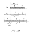
- FIG. 15B shows the misregistration errors in the integrated scenes prior to correction with time the shifted transfer gate signals of the present invention.
- FIG. 16A is a top view of a monochromatic piecewise linear CCD which shows how the present invention can be used to register the shifted monochromatic integrated scenes when there is a fractional lineskip for a selected resolution.
- FIG. 16B shows the misregistration error prior to correction with the time shifted transfer gate signals of the present invention.
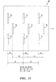
- FIG. 17 is a top view of a color multi-segmented piecewise linear CCD which shows how the present invention can be used to register a plurality of shifted color integrated scenes when there is a fractional lineskip between a leading and lagging photosensor for a selected resolution.
- FIG. 18 shows relationship between variable exposure controls and how teachings of the present invention can be applied to register a plurality of shifted color integrated scenes when misregistration errors occur as a result of variable color exposures during a scan.
- the present invention can be applied to a variety of image capturing systems and methods based on sensing systems comprising a plurality of photosensor arrays such as the photosensor arrays used in Charged Coupled Device technology, including, but not limited to, transmissive and reflective optical scanning systems, high resolution scanners, color digital cameras and color photocopying systems and the like.
- a photosensor array is a line sensor for scanning and capturing an electronic image from an original image; and that a plurality of photosensor arrays includes a CCD or CCD line sensing array.
- a sensing system employing a color trilinear CCD sensor essentially comprises three photosensor arrays, one array for each BGR color.
- FIGS. 1-3 are a schematic and partial representation of a prior art imaging system based on a trilinear color photosensor array or CCD platform, comprising a reflective flatbed scanner 1 having a glass plate surface 12, an illumination system essentially comprising a light source 14, an optical system essentially comprising a plurality of mirrors 16, a magnification system essentially comprising a lens 20, a movable CCD 40, and a linear drive system (not shown).
- An original 10 to be scanned is placed on the glass surface 12. The original is illuminated by the light source 14 and the resulting beam of light is reflected via the pathways as shown by arrows 30 onto the top surface of the CCD 40.
- FIGS. 2 and 3 illustrate, generally, how a trilinear CCD 40 having blue 46, green 44 and red 42 sensors comprises three rows of color integral filter stripes for spectral separation.
- FIG. 3 illustrates the pixel data sensed by the middle row 44, the green sensor array of light capturing elements.
- the CCD 40 is an analog solid state device that converts an amount of radiation falling thereon into a proportional voltage which is read and processed.
- the analog signals 35 from the CCD 40 are typically converted into digital data by a suitable Analog to Digital Converter.
- the digital data can then be further processed by known means to correct for imperfections in the light transmission and reflection, non-uniformity's in the CCD sensor elements and analog electronics, and then further processed through a number of image processing modules to achieve the desired resolution and quality.
- optical pixel length 9 ⁇ m is assumed for purposes of illustration. It will be readily understood by one skilled in the art that other CCDs may be illustrated where, for example, the optical line spacing is some other integer multiple of optical pixel lengths; the optical pixel size is a different length than 9 ⁇ m; and/or, the lead color sensor is for some other color than blue.
- magnification system employs a magnification ratio equal to one, and only resolution scans performed at a lower than optical resolution will be described. It will be readily understood by one skilled in the art that the present invention has applications to resolutions greater than optical resolution, and to imaging systems employing other magnification ratios.
- FIG. 4 diagrammatically illustrates a cross section of a prior art CCD 40 in the scanning direction (y-direction).
- the blue sensor 46 also known as the master sensor, is the lead sensor in the scanning direction, which is typically followed by the green sensor 44 and red sensor 42, respectively.
- the red 42 and green 44 color pixel sensor arrays, and the green 44 and blue 46 color pixel sensor arrays, are each separated by a channel 50 and 52, respectively.
- channels 50 and 52 are manufactured in equal lengths, each channel length 50 and 52 being equal to an integer number of optical pixel lengths.
- the lengths of channels 50 and 52 are shown as being equivalent to eleven optical pixel lengths (as indicated by hypothetical hash marks 51).
- each BGR photosensor array 42, 44 and 46 is also one pixel
- the optical line spacing between the red an green channels, OLS(R:G) 54 and OLS(G:B) 56 are each equivalent to twelve optical pixels in length
- the OLS(R:B) 110 is equivalent to twenty-four optical pixels in length.
- FIG. 5 diagrammatically illustrates how a scanning system having a CCD 40 with the above specifications performs an optical resolution scan in real time.
- the CCD 40 is shown in edgeview moving relative to the original 10 which is shown in topview.
- Scan lines R(N), G(N+12) and B(N+24) are the actively scanned lines at some incremental point in time, t N+24 .
- Each hash mark represents a 9 ⁇ m pixel length.
- FIG. 5 further shows the scan lines after N+24 lines of blue pixel data has been scanned.
- the currently scanned lines R(N), G(N+12) and B(N+24) are staggered by distances equal to the OLS(R:G) 54, (which in this example, is equivalent to OLS(G:B)) because of the timing of the common transfer gate signal and the uniform spacing of the CCD's BGR photosensor elements, 46, 44 and 42.
- the active scan line for the blue pixels B(N+24) is shifted by a distance equal to the OLS(G:B) 56 (12 optical pixel lengths or 108 ⁇ m) with respect to the scan line for the green pixel data G(N+12).
- the active scan line for the green pixels G(N+12) is shifted by the same OLS(R:G) 54 (12 optical pixel lengths or 108pm) with respect to the scan line for the red pixel data R(N).
- the scan line for the blue pixels B(N+24) is shifted by the OLS(R:B) 110 (24 optical pixel lengths or 216 ⁇ m) with respect to the scan line for the red pixel data R(N).
- FIG. 6A is a perspective view of FIG. 5 which illustrates the separate domains or integrated scenes for each color blue, green and red at time t 1 and t N+24 during the scan.
- Each integrated scene 60, 70, 80 contains the history of pixel data for a particular color as of a particular time (intensity values not shown).
- the original 10 is shown with optically sized 9 ⁇ m wide BGR scan lines L(N), L(N+12) and L(N+24), actively being scanned by CCD 40.
- the BGR integrated scenes 60, 70 and 80 are shown interposed between the original 10 and the CCD 40.
- the CCD 40 is schematically illustrated in two positions.
- the first position is at the beginning of the scan, t 1 , where line one, L(1), has been scanned for blue pixel data by the lead blue photosensor array 46.
- the blue integrated scene 80 consists of blue spectrally separated pixels from this single scan line, B(1), whereas the green and red integrated scenes have yet to accumulate any pixel information.
- the second position of CCD 40 is shown at a later point in time, t N+24 .
- t N N x T.
- t N+24 is N+24 units of linetime.
- the blue integrated scene 80 comprises N+24 lines of blue pixel data (lines B(1) through B(N+24).
- FIG. 6A further shows how at t N+24 the green integrated scene 70 comprises lines G(1) through G(N+12) of green pixel data and similarly, how the red integrated scene 60 comprises lines R(1) through R(N) of red pixel data.
- FIG. 6B is a schematic and edgeview of FIG. 6A.
- Vertical line 95 shows when an optical resolution scan is performed, the BGR pixel domains, 60, 70 and 80, are registered, i.e., they vertically align, left justified, as shown at 95.
- the first line scan for red R(1) vertically aligns with the first line scan for green G(1) and similarly, there is alignment with the first scan line for blue B(1).
- each of the scan lines R(N), G(N), and B(N) from integrated scenes 60, 70 and 80 respectively correspond to the Nth physical location with respect to the original 10.
- FIG. 6B further shows how with respect to diagonal line t N+24 , there is only enough real time data to image N lines of BGR scan lines.
- t N+24 As of t N+24 , notwithstanding the fact that N+24 blue lines have been scanned, only a full compliment of N blue, green and red scan lines may be imaged.
- the ability to output N lines of video data may be an important feature.
- the lineskip generally, is the quotient of the optical line spacing and the scanned pixel size. For a scan at optical resolution the lineskip is the interchannel or optical line spacing in units of scan lines. The lineskip represents the amount of lines necessary to skip so as to register the R, G and B scanned pixel data.
- B(N) can be accessed from the blue integrated scene 80 by counting back 24 lines, the lineskip(R:B), from the current blue scan line B(N+24).
- G(N) can be accessed from the green integrated scene 70 by counting back 12 lines, the lineskip(G:B) from G(N+12).
- R(N) can be accessed without counting back any lines.
- the lineskips provide a reference for registering scan lines.
- the integrated scenes for each color remain in a left justified alignment similar to those illustrated in FIG. 6B.
- the scanning resolution is reduced to half the optical resolution, i.e., from 4,000 to 2000 dpi, the scanning speed and hence the size of a scanned pixel is doubled from 9 ⁇ m to 18 ⁇ m so that the amount of pixel information sampled is cut in half.
- the optical line spacing between color sensors divided by the scanned pixel dimension remains equal to an integer value.
- the integrated scenes remain left justified and there is no color registration problem.
- the optical line spacing divided by the sampled pixel size equals an integer simple post processing and memory requirements may be used to correlate, or register, the shifted line scans for each color.
- the ratio of the scanned pixel length to the optical pixel length is 2.5 to 1.
- the relative lengths of the scanned pixels and optical pixels are shown as SP and OP, respectively, located above the original 10.
- FIG. 7 shows the beginning of a low resolution 1,600 dpi scan shown edgeview in the y-direction 100.
- Each line is represented by a pixel width in the y-dimension. Since the beginning of a scan is depicted in FIG. 7, only the blue 46 photosensor of the CCD 40 is shown beneath the original plane 10.
- the CCD 40 is shown at two positions in time t 4 and t 5 .
- the first position, POSITION A is at t 4 when the blue photosensor 46 has completed scanning line 4 with respect to the original plane 10.
- the green photosensor 44 has yet to reach the original plane 10.
- the end of integration of light for line 4, at t 4 is also the beginning of the integration of light for line 5.
- the 4 lines that have been integrated by the blue photosensor are shown as B 1 to B 4 of the blue integrated scene 80. From t 4 to t 5 , position A to B respectively, the blue photosensor 46 scans line 5 from the original and produces a blue line 5 as indicated by B 5 located immediately beneath the original 10
- a particular point in interest occurs at t 4 + 0.8T where the blue photosensor 46 has integrated 0.8 of the fifth line.
- the green photosensor 44 arrives at the beginning of the original 10, (line zero).
- the second position, POSITION B, is at t 5 , when the blue photosensor 46 is at the end of line 5 or the beginning of line 6 with respect to the original. At this point in time t 5 (5 units of linetime) the blue photosensor 46 will have integrated 5 blue scan lines. However, while the blue photosensor 46 is at the end of line 5 the green photosensor is at 0.2SP with respect to the original 10.
- FIG. 8 illustrates the scan of lines G(1) and B(6) respectively.
- the CCD 40 is shown at two positions in time, t 5 and t 6 .
- the first position, POSITION C is at t 5 This is the beginning of G(1) and B(6) respectively.
- the second position, POSITION D is at t 6 , when the green and blue photosensors are at the end of G(1) and B(6), respectively.
- the blue photosensor 46 has integrated 6 blue lines and the green photosensor 44 has integrated 1 green line.
- the green photosensor 42 will not begin to integrate light until it is at 0.2 of a scan line with respect to the original 10.
- ⁇ GB misregistration error
- ⁇ GB 1 - FRACTIONAL LINESKIP(G:B)
- ⁇ GB 1 - FRAC Optical Line Spacing (G:B) Scanned Pixel Size
- ⁇ GB 1 - FRAC(108 ⁇ m/22.5 ⁇ m)
- FIGS. 7-8 illustrate how the lineskip may be visualized as the number of scanned pixels which fit in the optical line spacing.
- 4.8 scanned pixels fit in the optical line spacing between the green and blue photosensors.
- the green sensor arrives at the beginning of line 1 out of synchronization with respect to the blue sensor's first scan B(1).
- the location of the green scan line G(1) is equal to the location of the blue scan line B(1) + ⁇ GB , where ⁇ GB is 0.2 of a scanned pixel length.
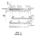
- FIG. 9 illustrates the scan of lines R(1), G(6) and B(11), respectively.
- the CCD 40 is shown at two positions in time, t 10 and t 11 .
- the first position, POSITION E, is at t 10 . This is the beginning of the integration of lines R(1), G(6) and B(11), respectively.
- the second position, POSITION F, is at t 11 . This is the end of the integration of lines R(1), G(6) and B(11), respectively.
- the integrated scenes for green 70 and blue 80 are shown below. Since the red sensor 42 is integrating its first line R(1) the red integrated scene 60 is not shown.
- misregistration between the red and blue integrated scenes ⁇ RB equals 0.4 scanned pixel length, or 9 ⁇ m.
- FIG. 10 shows in part the resulting BGR color integrated scenes 80, 70 and 60, respectively for a completed 1,600 dpi scan.
- the blue 80, green 70 and red 60 integrated scenes are shown in physical relation to the original 10.
- the original 10 has been marked off in optical pixel increments OP equal to 9 ⁇ m.
- a scanned pixel width is shown by SP as being equivalent to 2.5 optical pixels in length (22.5mm).
- FIG. 10 shows in part, how the misregistration errors ⁇ RG ⁇ GB , ⁇ RB cause the misregistration of scanned pixel data throughout the blue 80, green 70 and red 60 integrated scenes.
- the blue sensor 46 is integrating B(N) from t N-1 to t N
- the green sensor is integrating the G(N-5) from t N-1 to t N
- the red sensor is integrating the R(N-10) from t N-1 to t N .
- the blue sensor is integrating B(N)
- the green sensor is integrating the G(N-RULS(G:B))
- the red sensor is integrating the R(N-RULS(R:B)).
- RULS has been defined as the function which computes the round-up of the lineskip when there is a fractional component.
- the round-up of the green-blue lineskip, RULS(G:B), is the round-up of 4.8 which equals 5.
- the round-up of the red-blue lineskip RULS(R:B) is the round-up of 9.6 which equals 10.
- FIG. 10 further shows how at this 1,600 dpi resolution scan the amount of misregistration ⁇ GB between scan lines green G(N) and blue B(N) is equal to 0.2 of a scanned pixel length, or 4.5 ⁇ m, which is equivalent to half of an optical pixel length.
- the amount of misregistration ⁇ RB between scan lines green R(N) and blue B(N) is equal to 0.4 of a scanned pixel length, or 4.5 ⁇ m.
- Y G(N) Y B(N) + ⁇ GB
- ⁇ RB is the misregistration error between red and blue integrated scenes
- FIGS. 11A shows, generally, how the present invention overcomes the misregistration problem by providing three time shifted transfer gate signals 92, 94 and 96 for each BGR color sensor 42, 44 and 46 respectively.
- Each time shifted transfer gate signal 92, 94 and 96 has the same periodicity T equal to the linetime.
- the time shifted transfer gate signals are transmitted to a CCD having three independent transfer gate receiving means.
- CCDs having a plurality of independent transfer gate receiving means are known in the art.
- part no. KLI 10203 produced by the EASTMAN KODAK Company is a trilinear CCD having three lines of 10,200 CCD elements each line with its own built-in color filter (BGR).
- BGR built-in color filter
- This CCD has receiving means for separate configurable exposures for BGR.
- the CCD may be driven by any suitable clock means as timing generators and clock mechanisms are well known in the art.
- a CCD having independent transfer gate receiving means need not be triggered by individual transfer gate generators such as clock mechanisms and the like.
- a plurality of transfer gate signals with varying periods may be generated from harmonically related waveforms. In which case the above time-shifted transfer gate signals may be effectively generated by multiplexing the harmonics.
- any known microprocessor, oscillating device or clock means may be used to generate the transfer gate signals.
- the illustrated transfer gate signals are not intended to be limiting and may be generated by any equivalent means as known in the electronics art.
- each time shifted transfer gate signal triggers an independently timed line scan for a particular color.
- a first transfer gate signal BLUE TG signal 92
- BLUE TG signal 92 is directed to the blue transfer gate receiving means for triggering a scan with the blue sensor.
- a time shifted transfer gate signal for triggering the green sensor GREEN TG signal 94
- a time shifted transfer gate signal for the red sensor RED TG signal 96 is followed by a time shifted transfer gate signal for the red sensor RED TG signal 96.
- FIGS. 11A and 11B further show how, preferably, all three transfer gate signals are related through phase shifts with respect to time.
- the periodicity T of the transfer gate signals is equivalent to the linetime which is shown in FIGS. 11A and 11B as the distance between the leading edges of the timing pulses.
- FIG. 11B shows how when the CCD 40 has uniform optical line spacings, i.e., equal optical line spacing between photosensors, ⁇ is equal to 2 ⁇ .
- ⁇ is the amount of delay present in the GREEN TG signal so as to register the green and blue color pixels. In general, ⁇ is equal to the fractional lineskip times the period T of the transfer gate signal.
- FIGS. 12A and 12B compare an imaging system of the prior art with the imaging system and method of the present invention.
- FIG 12A shows how a prior art sensing system essentially comprising a trilinear photosensor array 40A has a common transfer gate receiving means BGR.
- BGR common transfer gate receiving means
- a common transfer gate signal TG(t) triggers all three photosensor arrays to scan simultaneously so that the shifted blue 80, green 70, and red 60 integrated scenes combine into a misregistered electronic image as shown.
- FIG 12B shows how a sensing system of the present invention essentially comprises a trilinear photosensor array 40B having three independent transfer gate receiving means B, G and R for receiving a blue, green and red transfer gate signal, respectively. Only the pin-outs for the independent transfer gate receiving means B, G and R are shown on the trilinear photosesnor array 40B.
- Three time shifted transfer gate signals TG( ⁇ (t- ⁇ )), TG( ⁇ (t- ⁇ ) and TG( ⁇ t) trigger each blue 46, green 44 and red 42 photosensor array to scan at shifted points in time, so that, the blue 80, green 70, and red 60 integrated scenes combine into a registered electronic image as shown.
- FIG. 12B is not intended to be limiting with respect to the number of photosensor arrays employed in the sensing system of the present invention.
- T- ⁇ is the amount of advance which is present in the GREEN TG signal so as to register the green and blue color pixels
- 2 x (T- ⁇ ) is the amount of advance present in the RED TG signal required to register the red and blue pixels.
- BLUE TG signal 92 is some periodic timing signal as a function of time
- the lineskip may be computed as the quotient of the optical line spacing and the scanned pixel size in units of optical pixel lengths.
- LINESKIP Optical Line Spacing [Optical Pixel lengths] Size of the Scanned Pixel [Opt. Pixel lengths]
- the lineskip may be calculated in terms of the optical line spacing, optical and scanning resolutions as shown.
- LINESKIP Optical Line Spacing x Scanning Resolution Optical Resolution
- the OLS between green 44 and blue 46 CCD sensors is 12 optical pixel lengths.
- Table 1 has a plurality of resolutions where the lineskips have been calculated according to the above formulas.
- the lineskip is broken into two columns for each pair of color sensors.
- the column designated INTEGER is the integer component of the lineskip
- the column designated FRACTIONAL is the fractional component of the lineskip.
- the lineskip for a particular scan is equal to the sum of the two columns.
- the time delays ⁇ and ⁇ for the green and red transfer gate signals may be readily computed by multiplying the decimal fraction in the fractional column by the period of the transfer gate signal T.
- TG( ⁇ t) is the transfer gate signal for a leading photosensor array K then TG( ⁇ (t - ⁇ K+1 )) will register the integrated scene produced by the lagging photosensor K+1 with the integrated scene produced by the leading photosensor K.
- the blue and green, or blue and red photosensor arrays may be triggered with time shifted transfer gate signals.
- FIG. 15A shows how the teachings of the present invention allows CCD designs of differing optical line spacings.
- the teachings of the present invention allow for optical line spacings which are not integer multiples of optical pixel lengths. It will be further appreciated that the optical line spacing between photosensor arrays does not have to be uniform.
- FIG. 15A shows a CCD having both non-integer and nonuniform optical line spacings between leading and lagging photosensor arrays (Pin-outs not shown).
- FIG. 15A shows a color CCD array having a green-blue optical line spacing OLS(G:B) and a red-green optical line spacing OLS(R:G) equal to 72.9 ⁇ m and 118 ⁇ m, respectively.
- OLS(G:B) green-blue optical line spacing
- R:G red-green optical line spacing
- FIG. 16A shows how, for example, the teachings of the present invention may be readily applied to monochromatic imaging systems which utilize piece-wise linear CCD arrays.
- the CCD 140 comprises three piece-wise linear photosensor segments 142, 144 and 146 respectively (Pin-outs not shown). In this example, segments 142 and 146 align in the x-direction while the lead sensor segment 144 extends in the direction of the scan.
- the optical line spacing is the distance between segments 142 and 144 or equivalently 146 and 144.
- the lineskip between either lagging photosensor 142 or 146 and leading photosensor 144 equals the optical line spacing S divided by the scanned pixel size.
- the fractional lineskip is the fractional component of the lineskip.
- FIG. 16B shows qualitatively, for a resolution in which the lineskip has a fractional component that is not corrected for in accordance with the teachings of the present invention
- the scanned pixels for segments 142 and 146 will be shifted with respect to the pixels scanned by the middle segment 144.
- the amount of shift or misregistration is shown qualitatively as ⁇ S .
- FIG. 17 shows a color CCD 340 comprising three color segmented arrays R, G and B where each segmented array is in a similar piecewise linear configuration as above (Pin-outs not shown).
- the red photosensor segment R consists of red photosensor arrays R 1 , R 2 , R 3
- the green photosensor segment G consists of green photosensor arrays G 1 , G 2 , G 3
- the blue photosensor segment B consists of blue photosensor arrays B 1 , B 2 , B 3 .
- R 1 aligns with R 3
- G 1 aligns with G 3
- B 1 aligns with B 3
- the optical line spacing between any pair of adjacent photosensors in the y-dimension is uniform. Therefore, for example, the optical line spacing between R 1 and G 1 OLS(R 1 :G 1 ) is equal to the optical line spacing between G 1 and B 1 OLS(G 1 :B 1 ) and in general, OLS(R i :G i ) equals OLS(G i :B i ).
- Table 2 shows, for an imaging system having an optical resolution of 4,000 dpi, an optical line spacing between color sensors of the same index equal to 12 optical pixel lengths and an optical line spacing between offset photosensors (B 1 and B 2 , and B 2 and B 3 ) equal to 3 optical pixel lengths, that for a scan at 1,600 dpi the following set of transfer gate signals will correct the misregistration error.
- FIG. 18 shows how the present invention can be applied to color misregistration errors caused by automatic exposure controls.
- blue, green and red sensors have different sensitivities to light. For example, blue sensors are less sensitive to light than green or red sensors. Typically, this requires that the blue sensor has a longer exposure period for integrating light during a linetime than the exposure periods for the green or red sensors.
- FIG. 18 shows how an automatic exposure control causes the center of a blue pixel 250 to be shifted with respect to the corresponding center of a green 252 or red 254 pixel.
- R, G, B represent the scanned pixel size when there is no adjustment in the exposure and thus the exposure period equals the linetime.
- the pixel sizes in relation to their respective exposure periods are represented by segments RE, GE, and BE, respectively.
- the differences in exposure times causes a misregistration problem by shifting the center of each color pixel as indicated by the positions of 250, 252, and 254, respectively.
- the optical line spacing divided by the scanned pixel size is an integer, e.g., during an optical scan, integrated scenes or the domains for the blue, green and red pixel data are shifted due to the differences in exposure times for each color sensor.
- the misregistration caused by the nonuniform exposure periods for each color may be solved by the present invention's teachings of time-shifting transfer gate signals.
- FIG. 17 where it is assumed that the exposure time for the blue sensor equals the linetime, there is only the need to time-shift the green and red transfer gate signals.
- the teachings of the present invention correct for variable exposure settings by time shifting the appropriate transfer gate signals a fraction of the linetime corresponding to the duration of nonexposure divided by two, thereby aligning the center gravity for each color pixel.
- the duration of nonexposure corresponds to a segment of nonexposure ⁇ NE within the scanned pixel where light is not exposed to the corresponding sensor as indicated by ⁇ GNE and G RNE , for the green and red pixels, respectively.
- One way to correct for the shift in pixel center gravity due to variable exposure times is to advance each color signal by an amount of time which corresponds to the nonexposure period divided by two, ( ⁇ GNE/2 ), ( ⁇ RNE/2 ).
- a time shift may consist of a delay or an equivalent advance in the transfer gate signals.
- a leading photosensor array may be shifted with respect to time as opposed to a lagging photosensor array by selecting a lagging photosensor as the reference sensor.
- teachings of the present invention allow for CCDs to be employed with optical line spacings that are neither uniform nor an integer number of pixels in length.
- the present invention allows for CCDs to be used which have a combination of nonuniform and non-integer optical line spacings.
- the correction for the misregistration error caused by a fractional lineskip at a particular resolution may not be perfect since the fractional component of the optical line spacing divided by the scanned pixel size may be a long decimal equivalent with a number of insignificant digits which exceeds the accuracy of the imaging system.
- Such examples include, but are not limited to, fractional lineskips that have long repeating decimals and irrational numbers; in which event, small round off errors may exist in the registration.
Landscapes
- Engineering & Computer Science (AREA)
- Multimedia (AREA)
- Signal Processing (AREA)
- Facsimile Scanning Arrangements (AREA)
- Facsimile Heads (AREA)
- Color Electrophotography (AREA)
- Color Image Communication Systems (AREA)
- Transforming Light Signals Into Electric Signals (AREA)
Applications Claiming Priority (2)
| Application Number | Priority Date | Filing Date | Title |
|---|---|---|---|
| US33449 | 1987-04-01 | ||
| US09/033,449 US6075236A (en) | 1998-03-02 | 1998-03-02 | Registration apparatus and method for imaging at variable resolutions |
Publications (2)
| Publication Number | Publication Date |
|---|---|
| EP0940973A2 true EP0940973A2 (fr) | 1999-09-08 |
| EP0940973A3 EP0940973A3 (fr) | 2002-08-21 |
Family
ID=21870471
Family Applications (1)
| Application Number | Title | Priority Date | Filing Date |
|---|---|---|---|
| EP99200470A Withdrawn EP0940973A3 (fr) | 1998-03-02 | 1999-02-18 | Appareil de régistration et procédé d'imagerie à résolution variable |
Country Status (3)
| Country | Link |
|---|---|
| US (1) | US6075236A (fr) |
| EP (1) | EP0940973A3 (fr) |
| JP (1) | JPH11313194A (fr) |
Families Citing this family (7)
| Publication number | Priority date | Publication date | Assignee | Title |
|---|---|---|---|---|
| TW477958B (en) * | 1999-09-30 | 2002-03-01 | Umax Data Systems Inc | Point taking method of digital image capture system and its device |
| TW525369B (en) * | 2001-08-03 | 2003-03-21 | Veutron Corp | Scanning method |
| CA2369710C (fr) * | 2002-01-30 | 2006-09-19 | Anup Basu | Methode et appareil pour le balayage 3d a haute resolution d'objets comprenant des vides |
| US20030222987A1 (en) * | 2002-05-30 | 2003-12-04 | Karazuba Paul M. | Line scan image recording device with internal system for delaying signals from multiple photosensor arrays |
| US7746514B2 (en) * | 2004-04-14 | 2010-06-29 | Hung-Yi Hsu | Scanner and exposure control method thereof |
| KR101590881B1 (ko) * | 2008-12-24 | 2016-02-02 | 삼성전자 주식회사 | 화상처리장치 및 그 제어방법 |
| US8587841B2 (en) * | 2011-11-16 | 2013-11-19 | Eastman Kodak Company | Compact configuration for a scan bar assembly |
Family Cites Families (7)
| Publication number | Priority date | Publication date | Assignee | Title |
|---|---|---|---|---|
| US4278995A (en) * | 1979-08-20 | 1981-07-14 | Eastman Kodak Company | Color line sensor for use in film scanning apparatus |
| US4641185A (en) * | 1984-12-18 | 1987-02-03 | Polaroid Corporation | Image sensing and processing apparatus and method |
| JPH0620221B2 (ja) * | 1987-07-15 | 1994-03-16 | 大日本スクリ−ン製造株式会社 | 読取りタイミングを相対的にずらせた画像読取り装置 |
| US5191409A (en) * | 1988-03-29 | 1993-03-02 | Mitsubishi Denki Kabushiki Kaisha | Color scanning system |
| JPH0435177A (ja) * | 1990-05-25 | 1992-02-05 | Suzuki Motor Corp | Ccd駆動回路 |
| US5440343A (en) * | 1994-02-28 | 1995-08-08 | Eastman Kodak Company | Motion/still electronic image sensing apparatus |
| JP3847811B2 (ja) * | 1995-06-30 | 2006-11-22 | キヤノン株式会社 | 撮像装置 |
-
1998
- 1998-03-02 US US09/033,449 patent/US6075236A/en not_active Expired - Fee Related
-
1999
- 1999-02-18 EP EP99200470A patent/EP0940973A3/fr not_active Withdrawn
- 1999-02-26 JP JP11051256A patent/JPH11313194A/ja active Pending
Also Published As
| Publication number | Publication date |
|---|---|
| JPH11313194A (ja) | 1999-11-09 |
| US6075236A (en) | 2000-06-13 |
| EP0940973A3 (fr) | 2002-08-21 |
Similar Documents
| Publication | Publication Date | Title |
|---|---|---|
| US8129760B2 (en) | Image sensor and image reading apparatus | |
| US5750985A (en) | High speed and high precisioin image scanning apparatus | |
| US5075768A (en) | Method and apparatus for color separation scanning | |
| EP0940973A2 (fr) | Appareil de régistration et procédé d'imagerie à résolution variable | |
| JPS63156474A (ja) | 読取装置 | |
| EP0273638B1 (fr) | Systèmes d'analyse d'images | |
| US6175429B1 (en) | Document reader and method for adjusting its focus | |
| JP2000083132A (ja) | カラ―撮像装置およびそれを用いた画像読み取り装置 | |
| JPS60154244A (ja) | 写真画像情報検出装置 | |
| JP3487718B2 (ja) | 画像形成装置 | |
| EP0070620A2 (fr) | Dispositif de formation d'image à haute densité | |
| JP3139102B2 (ja) | 画像読取装置 | |
| US7605958B2 (en) | Design parameters for a multi-row linear photosensor array | |
| JPH1051628A (ja) | 画像読取装置 | |
| JPH1079836A (ja) | 画像読取装置 | |
| EP1148710A2 (fr) | Eléments de lecture d'images en couleurs, appareil de lecture d'images avec éléments de lecture d'images, et procédé de lecture d'image | |
| JP3041020B2 (ja) | 読取装置と読取方法 | |
| JPH08251347A (ja) | 同期加算式カラーリニアイメージセンサ | |
| EP0357177B1 (fr) | Procédé et appareil pour balayage par séparation de couleurs | |
| JP2000232565A (ja) | 複数光センサ列走査装置 | |
| JP2002199171A (ja) | カラー画像読取装置 | |
| JPH0457455A (ja) | 画像読取装置 | |
| JPH08214114A (ja) | 画像読取装置 | |
| JPH08107472A (ja) | 画像読み取り装置 | |
| JPS62241467A (ja) | カラ−イメ−ジセンサ− |
Legal Events
| Date | Code | Title | Description |
|---|---|---|---|
| PUAI | Public reference made under article 153(3) epc to a published international application that has entered the european phase |
Free format text: ORIGINAL CODE: 0009012 |
|
| AK | Designated contracting states |
Kind code of ref document: A2 Designated state(s): AT BE CH CY DE DK ES FI FR GB GR IE IT LI LU MC NL PT SE |
|
| AX | Request for extension of the european patent |
Free format text: AL;LT;LV;MK;RO;SI |
|
| PUAL | Search report despatched |
Free format text: ORIGINAL CODE: 0009013 |
|
| AK | Designated contracting states |
Kind code of ref document: A3 Designated state(s): AT BE CH CY DE DK ES FI FR GB GR IE IT LI LU MC NL PT SE |
|
| AX | Request for extension of the european patent |
Free format text: AL;LT;LV;MK;RO;SI |
|
| 17P | Request for examination filed |
Effective date: 20030221 |
|
| AKX | Designation fees paid |
Designated state(s): DE FR GB |
|
| 17Q | First examination report despatched |
Effective date: 20030618 |
|
| STAA | Information on the status of an ep patent application or granted ep patent |
Free format text: STATUS: THE APPLICATION IS DEEMED TO BE WITHDRAWN |
|
| 18D | Application deemed to be withdrawn |
Effective date: 20031230 |