EP0942302A2 - Module électrooptique - Google Patents
Module électrooptique Download PDFInfo
- Publication number
- EP0942302A2 EP0942302A2 EP98117620A EP98117620A EP0942302A2 EP 0942302 A2 EP0942302 A2 EP 0942302A2 EP 98117620 A EP98117620 A EP 98117620A EP 98117620 A EP98117620 A EP 98117620A EP 0942302 A2 EP0942302 A2 EP 0942302A2
- Authority
- EP
- European Patent Office
- Prior art keywords
- broad side
- module according
- transmission
- lens
- coupling
- Prior art date
- Legal status (The legal status is an assumption and is not a legal conclusion. Google has not performed a legal analysis and makes no representation as to the accuracy of the status listed.)
- Withdrawn
Links
Images

Classifications
-
- H—ELECTRICITY
- H01—ELECTRIC ELEMENTS
- H01S—DEVICES USING THE PROCESS OF LIGHT AMPLIFICATION BY STIMULATED EMISSION OF RADIATION [LASER] TO AMPLIFY OR GENERATE LIGHT; DEVICES USING STIMULATED EMISSION OF ELECTROMAGNETIC RADIATION IN WAVE RANGES OTHER THAN OPTICAL
- H01S5/00—Semiconductor lasers
- H01S5/02—Structural details or components not essential to laser action
- H01S5/022—Mountings; Housings
- H01S5/023—Mount members, e.g. sub-mount members
-
- G—PHYSICS
- G02—OPTICS
- G02B—OPTICAL ELEMENTS, SYSTEMS OR APPARATUS
- G02B6/00—Light guides; Structural details of arrangements comprising light guides and other optical elements, e.g. couplings
- G02B6/24—Coupling light guides
- G02B6/42—Coupling light guides with opto-electronic elements
- G02B6/4201—Packages, e.g. shape, construction, internal or external details
- G02B6/4246—Bidirectionally operating package structures
-
- G—PHYSICS
- G02—OPTICS
- G02B—OPTICAL ELEMENTS, SYSTEMS OR APPARATUS
- G02B6/00—Light guides; Structural details of arrangements comprising light guides and other optical elements, e.g. couplings
- G02B6/24—Coupling light guides
- G02B6/42—Coupling light guides with opto-electronic elements
- G02B6/4201—Packages, e.g. shape, construction, internal or external details
- G02B6/4204—Packages, e.g. shape, construction, internal or external details the coupling comprising intermediate optical elements, e.g. lenses, holograms
- G02B6/4214—Packages, e.g. shape, construction, internal or external details the coupling comprising intermediate optical elements, e.g. lenses, holograms the intermediate optical element having redirecting reflective means, e.g. mirrors, prisms for deflecting the radiation from horizontal to down- or upward direction toward a device
-
- H—ELECTRICITY
- H01—ELECTRIC ELEMENTS
- H01S—DEVICES USING THE PROCESS OF LIGHT AMPLIFICATION BY STIMULATED EMISSION OF RADIATION [LASER] TO AMPLIFY OR GENERATE LIGHT; DEVICES USING STIMULATED EMISSION OF ELECTROMAGNETIC RADIATION IN WAVE RANGES OTHER THAN OPTICAL
- H01S5/00—Semiconductor lasers
- H01S5/02—Structural details or components not essential to laser action
- H01S5/022—Mountings; Housings
- H01S5/0233—Mounting configuration of laser chips
-
- H—ELECTRICITY
- H01—ELECTRIC ELEMENTS
- H01S—DEVICES USING THE PROCESS OF LIGHT AMPLIFICATION BY STIMULATED EMISSION OF RADIATION [LASER] TO AMPLIFY OR GENERATE LIGHT; DEVICES USING STIMULATED EMISSION OF ELECTROMAGNETIC RADIATION IN WAVE RANGES OTHER THAN OPTICAL
- H01S5/00—Semiconductor lasers
- H01S5/02—Structural details or components not essential to laser action
- H01S5/022—Mountings; Housings
- H01S5/0235—Method for mounting laser chips
-
- G—PHYSICS
- G02—OPTICS
- G02B—OPTICAL ELEMENTS, SYSTEMS OR APPARATUS
- G02B6/00—Light guides; Structural details of arrangements comprising light guides and other optical elements, e.g. couplings
- G02B6/24—Coupling light guides
- G02B6/42—Coupling light guides with opto-electronic elements
- G02B6/4201—Packages, e.g. shape, construction, internal or external details
- G02B6/4204—Packages, e.g. shape, construction, internal or external details the coupling comprising intermediate optical elements, e.g. lenses, holograms
- G02B6/4207—Packages, e.g. shape, construction, internal or external details the coupling comprising intermediate optical elements, e.g. lenses, holograms with optical elements reducing the sensitivity to optical feedback
-
- G—PHYSICS
- G02—OPTICS
- G02B—OPTICAL ELEMENTS, SYSTEMS OR APPARATUS
- G02B6/00—Light guides; Structural details of arrangements comprising light guides and other optical elements, e.g. couplings
- G02B6/24—Coupling light guides
- G02B6/42—Coupling light guides with opto-electronic elements
- G02B6/4201—Packages, e.g. shape, construction, internal or external details
- G02B6/4204—Packages, e.g. shape, construction, internal or external details the coupling comprising intermediate optical elements, e.g. lenses, holograms
- G02B6/4215—Packages, e.g. shape, construction, internal or external details the coupling comprising intermediate optical elements, e.g. lenses, holograms the intermediate optical elements being wavelength selective optical elements, e.g. variable wavelength optical modules or wavelength lockers
-
- G—PHYSICS
- G02—OPTICS
- G02B—OPTICAL ELEMENTS, SYSTEMS OR APPARATUS
- G02B6/00—Light guides; Structural details of arrangements comprising light guides and other optical elements, e.g. couplings
- G02B6/24—Coupling light guides
- G02B6/42—Coupling light guides with opto-electronic elements
- G02B6/4201—Packages, e.g. shape, construction, internal or external details
- G02B6/4219—Mechanical fixtures for holding or positioning the elements relative to each other in the couplings; Alignment methods for the elements, e.g. measuring or observing methods especially used therefor
- G02B6/4236—Fixing or mounting methods of the aligned elements
- G02B6/424—Mounting of the optical light guide
-
- G—PHYSICS
- G02—OPTICS
- G02B—OPTICAL ELEMENTS, SYSTEMS OR APPARATUS
- G02B6/00—Light guides; Structural details of arrangements comprising light guides and other optical elements, e.g. couplings
- G02B6/24—Coupling light guides
- G02B6/42—Coupling light guides with opto-electronic elements
- G02B6/4201—Packages, e.g. shape, construction, internal or external details
- G02B6/4251—Sealed packages
- G02B6/4253—Sealed packages by embedding housing components in an adhesive or a polymer material
-
- G—PHYSICS
- G02—OPTICS
- G02B—OPTICAL ELEMENTS, SYSTEMS OR APPARATUS
- G02B6/00—Light guides; Structural details of arrangements comprising light guides and other optical elements, e.g. couplings
- G02B6/24—Coupling light guides
- G02B6/42—Coupling light guides with opto-electronic elements
- G02B6/4201—Packages, e.g. shape, construction, internal or external details
- G02B6/4256—Details of housings
- G02B6/4257—Details of housings having a supporting carrier or a mounting substrate or a mounting plate
- G02B6/4259—Details of housings having a supporting carrier or a mounting substrate or a mounting plate of the transparent type
-
- G—PHYSICS
- G02—OPTICS
- G02B—OPTICAL ELEMENTS, SYSTEMS OR APPARATUS
- G02B6/00—Light guides; Structural details of arrangements comprising light guides and other optical elements, e.g. couplings
- G02B6/24—Coupling light guides
- G02B6/42—Coupling light guides with opto-electronic elements
- G02B6/4201—Packages, e.g. shape, construction, internal or external details
- G02B6/4286—Optical modules with optical power monitoring
-
- H—ELECTRICITY
- H01—ELECTRIC ELEMENTS
- H01S—DEVICES USING THE PROCESS OF LIGHT AMPLIFICATION BY STIMULATED EMISSION OF RADIATION [LASER] TO AMPLIFY OR GENERATE LIGHT; DEVICES USING STIMULATED EMISSION OF ELECTROMAGNETIC RADIATION IN WAVE RANGES OTHER THAN OPTICAL
- H01S5/00—Semiconductor lasers
- H01S5/02—Structural details or components not essential to laser action
- H01S5/022—Mountings; Housings
- H01S5/0225—Out-coupling of light
- H01S5/02251—Out-coupling of light using optical fibres
-
- H—ELECTRICITY
- H01—ELECTRIC ELEMENTS
- H01S—DEVICES USING THE PROCESS OF LIGHT AMPLIFICATION BY STIMULATED EMISSION OF RADIATION [LASER] TO AMPLIFY OR GENERATE LIGHT; DEVICES USING STIMULATED EMISSION OF ELECTROMAGNETIC RADIATION IN WAVE RANGES OTHER THAN OPTICAL
- H01S5/00—Semiconductor lasers
- H01S5/02—Structural details or components not essential to laser action
- H01S5/022—Mountings; Housings
- H01S5/0225—Out-coupling of light
- H01S5/02255—Out-coupling of light using beam deflecting elements
-
- H—ELECTRICITY
- H01—ELECTRIC ELEMENTS
- H01S—DEVICES USING THE PROCESS OF LIGHT AMPLIFICATION BY STIMULATED EMISSION OF RADIATION [LASER] TO AMPLIFY OR GENERATE LIGHT; DEVICES USING STIMULATED EMISSION OF ELECTROMAGNETIC RADIATION IN WAVE RANGES OTHER THAN OPTICAL
- H01S5/00—Semiconductor lasers
- H01S5/02—Structural details or components not essential to laser action
- H01S5/022—Mountings; Housings
- H01S5/023—Mount members, e.g. sub-mount members
- H01S5/02325—Mechanically integrated components on mount members or optical micro-benches
-
- H—ELECTRICITY
- H01—ELECTRIC ELEMENTS
- H01S—DEVICES USING THE PROCESS OF LIGHT AMPLIFICATION BY STIMULATED EMISSION OF RADIATION [LASER] TO AMPLIFY OR GENERATE LIGHT; DEVICES USING STIMULATED EMISSION OF ELECTROMAGNETIC RADIATION IN WAVE RANGES OTHER THAN OPTICAL
- H01S5/00—Semiconductor lasers
- H01S5/06—Arrangements for controlling the laser output parameters, e.g. by operating on the active medium
- H01S5/068—Stabilisation of laser output parameters
- H01S5/0683—Stabilisation of laser output parameters by monitoring the optical output parameters
Definitions
- the invention is based on the genus, as in independent claim 1 specified.
- Such a module is from the German patent DE 195 27 026 C2 known.
- the invention is concerned with a module, in particular with an optical transceiver that can be installed in a Receptacle is suitable for leadframe assembly technology.
- a Receptacle proposed for leadframe assembly technology.
- an edge emitting Semiconductor laser diode with integrated beam transformation prefers.
- Such semiconductor laser diodes have in Direction of light propagation after the active laser channel the same chip a passive Transformation waveguide, the mode field diameter of the laser enlarged from approx. 1 ⁇ m to approx. 4.5 ⁇ m and thus a better adaptation to the mode field diameter of a Single mode fiber of 10 ⁇ m enables.
- this beam transformation the beam angle of approx. 30 ° reduced to about 12 °.
- SSC laser spot size converted laser diode
- the laser shines in one on his End face arranged at a short distance (End face coupling).
- the fiber axis must be in the Mounting level (emission direction) of the laser.
- the laser can cause back reflections on the face of the fiber disturbed in its radiation characteristics become.
- a transceiver that is in addition to a Transmitting element (e.g. transmitting laser) still a receiving element (e.g. photodiode) can also be used in a Direct coupling of the fiber to the laser because of the required small distance between the End faces of laser and fiber no beam splitting Element for separating the transmission radiation from the reception radiation accommodate.
- a Transmitting element e.g. transmitting laser
- a receiving element e.g. photodiode
- the subject of the application with the features of claim 1 has the following advantage:
- the module is suitable for installation in a receptacle and can be manufactured inexpensively for large-scale use. It can be designed as a transmitter module or transceiver.
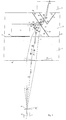
- a first silicon substrate 1 with plane-parallel broad sides 11, 14 carries, on a first broad side 11 as a transmission component 12, a transmission laser which is fastened with the aid of a mounting layer 13.
- the beam emerging from the light exit surface 120 on the end face of the transmission laser 12 with the center beam 121 at the transmission wavelength ⁇ 1 strikes an inclined surface 21.
- This surface is preferably generated by an anisotropic etching process in a second silicon substrate 2.
- the structuring of the second silicon substrate 2 can advantageously be done by structuring a silicon wafer in multiple uses. Only one use is shown in FIG. 1.
- n 0 is the refractive index in the space between the first broad side 11 of the substrate 1, the filter layer 22 and the light exit surface 120.
- This space can be filled with air in a first embodiment of the invention (case 1) or with a transparent adhesive in a second embodiment (case 2).
- the first broad side 11 is covered with an antireflection layer at least in the area of the beam entrance.
- a lens 15 is provided on the second broad side 14 of the substrate 1 as a structured surface area for focusing the transmission beam.
- this lens is structured as an integrated lens directly on the silicon substrate 1 in multiple uses.
- the surface of the lens is covered with an anti-reflection layer.
- This lens has the task of converting the diverging beam bundle emerging from the laser into a converging beam bundle and thereby imaging the light exit surface 120 onto a coupling surface within the end face 42 of an optical fiber 4 (namely in the core 41).
- an angle ⁇ 4 must be included between the normal to the end face 42 and the direction of the center beam 124 of the converging beam, which is greater than the angle of convergence between the center beam and an edge beam of the converging beam.
- an incident beam must also be coupled in at an angle to the fiber axis in order to avoid coupling losses due to angular misalignment.
- the axis of the socket and thus also an inserted plug must be guided perpendicular to the mounting surface of the receptacle.
- the magnification ratio for the beam transformation can be set by selecting the radius of curvature.
- the beam emerging from the semiconductor laser which can be regarded approximately as a Gaussian beam, is transformed such that the waist of the transformed laser beam is as large as the beam waist of a light wave guided in the single-mode fiber.
- LD laser diode
- R K 1100 ⁇ m Radius of the Si lens
- g 649 ⁇ m optical path lens - fiber (image width)
- b 1404 ⁇ m
- the waist size and the beam direction can be chosen by choosing the lens curvature radius R K of 1100 ⁇ m or 825 ⁇ m and the lens offset ⁇ X Li of 120 ⁇ m or 147 ⁇ m adjust that an optimal coupling into a single-mode fiber aligned perpendicular to the mounting plane of the laser is possible.
- the calculation for the propagation of the beams is also valid for the reverse light path according to the reciprocity principle of optics.
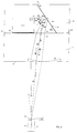
- the dichroic filter layer 22 has a very low reflectivity and a very high transmittance for the received beam because of its different wavelength.
- the received beam is therefore not reflected here, but rather enters the interior of the silicon substrate 2.
- the receiving beam is broken to the plumb line on the surface 21.
- an anisotropically etched recess 3 is produced in the side 24 of the substrate 2 in accordance with a development of the invention.
- the received light beam with the center beam 131 strikes the side surface 31 of the recess 3. Since the two surfaces 21 and 31 are parallel to one another because of the same anisotropic etching process, the angle of incidence ⁇ is for the two cases with air or a transparent adhesive on the left side of the surface 21 3L or ⁇ 3K of the center beam 131 on the boundary surface 31 is as large as the refraction angle ⁇ 2L or ⁇ 2K on the right side of the surface 21.
- the angle of incidence is smaller than the critical angle of total reflection, so that the light can emerge from the silicon substrate .
- this surface is covered with an anti-reflection layer 32.
- the same filter layer as in layer 22 can also be used here. In this case, both sides of the silicon wafer 2 can be coated in the same vacuum process.
- the recess 3 can either with air or with be filled with a transparent adhesive. Depending on Refractive index in the recess 3 result for the Refractive angles of the two cases 1 and 2 following Combinations:
- a photodiode can be used the active area on the top, as in FIG. 1 shown, or a photodiode with the active area the bottom can be used.
- the lateral position the photodiode can use the above Direction angle and the position of the recess 3 predetermined with respect to area 21 and by marks or latching structures on the side 24 of the silicon substrate 2 are marked, so that a passive Adjustment of this receiving diode is possible.
- the transformed receiving beam waist at point P 5 then has the same diameter as the beam waist of the laser beam at the light exit surface at point P 0 of the laser. In the example given, this is 4.5 ⁇ m. This means that even small-area photodiodes that are required for the highest frequency ranges (diameter of the active zone typically 30 ⁇ m) can still be coupled with sufficient adjustment latitude.
- the assembly of the optoelectronic Transducer elements can also be inexpensive Wafer level.
- the mutual orientation of the Upper and lower silicon substrates can advantageously happen at the wafer level. Doing so with all sub-substrates of both in a single adjustment process Wafers aligned with each other at the same time. This Alignment can also be done without adjustment if on the Wafers at least two places to each other corresponding locking structures together with the anisotropic etching of the other structures become.
- These locking structures can, for example be pyramid-shaped recesses, into which precision balls be inserted.
- the mutual fixation of the Both wafers can be glued, soldered or another known fastening method happen. After Fixation, the wafers are separated and the individual Module blocks mounted on the lead frames.
- FIG. 2 shows an inventive transceiver module that is mounted on one side 201 of a lead frame 200.
- Socket 300 On the other side 202 of leadframe 200 is one Socket 300 actively adjusted with its flange surface 301 and fixed via laser welding spots 203.
- the socket is a ferrule 400 with the transmission fiber 4 introduced.
- This fiber has an oblique cut Face (the cutting angle in this Embodiment is 8 °) in which the transformed Laser beam 124 is coupled.
- the axial distance will be preset by the stop ring 310 so that between the lens 15 on the underside 14 of the Silicon substrate 1 and the waist of the transformed Laser beam 124 just the image width calculated above b lies.
- the lateral position of the fiber with respect to the Beam waist of the transformed laser beam is through active adjustment of the flange surface 301 on the underside 202 of the leadframe 200 set and by laser welding spots 203 fixed.
- the one emerging from the back of the laser chip Light signal can, as is customary in the prior art, can be used for power control.
- the structure according to the invention offers an advantageous one for this Solution for beam deflection on a planar mounted Monitor diode 60.
- This monitor diode is invented mounted in a recess 16 in the silicon substrate 1.
- the top silicon substrate 2 receives another anisotropic etched surface 61 opposite surface 21.
- Both Surfaces 21 and 61 are the side surfaces of anisotropic etched opening 20 in the upper silicon substrate 2.
- the beam deflection of the rear emerging Laser beam is done by reflection on surface 61, for this purpose with a reflecting the laser wavelength Layer 62 is occupied.
- This can advantageously Layer 62 have the same structure as that dichroic layer 22 on the surface 21 and with it produced together without significant additional effort become.
- the bottom of the monitor diode 60 becomes the bottom and at least one of the side surfaces of the recess 16 with a gold layer 17 occupied.
- the rest of the electrical Contacting the receiving and transmitting branch of the Transceiver module is done via bond wires to the corresponding contact areas of the leadframe (not here drawn).
- the active components of the transceiver and the bond wires with an optically transparent protective potting compound top) 70 The entire module can then still be used surrounded by a hard covering (not shown here) become.
- an integrated transceiver chip 512 (FIG. 3) can also be used.
- a transceiver chip contains, integrated on a chip, a transmission part which emits the wavelength ⁇ 1 and a reception part which receives the reception wavelength ⁇ 2 .
- the transmitted and received light are routed via the same input and output waveguide on the chip and have the same light entry and exit spot that is located at point P 0 .
- this common input and output waveguide can be designed as a transformation waveguide to enlarge the mode field diameter.
- the beam paths for the send and receive directions are then as previously described for the send direction.
- the dichroic filter layer 22 is now replaced by a reflection layer 522 for both wavelengths.
- the wavelengths are separated on the integrated transceiver chip by an integrated wavelength-selective coupler.
- the transceiver chip can also contain an integrated monitor diode, so that the monitor diode 60 according to FIG. 2 in the recess 16 with the surface 61 provided for beam deflection can be omitted.
Landscapes
- Physics & Mathematics (AREA)
- General Physics & Mathematics (AREA)
- Optics & Photonics (AREA)
- Condensed Matter Physics & Semiconductors (AREA)
- Electromagnetism (AREA)
- Optical Couplings Of Light Guides (AREA)
Applications Claiming Priority (2)
| Application Number | Priority Date | Filing Date | Title |
|---|---|---|---|
| DE19810624A DE19810624A1 (de) | 1998-03-12 | 1998-03-12 | Elektrooptisches Modul |
| DE19810624 | 1998-03-12 |
Publications (2)
| Publication Number | Publication Date |
|---|---|
| EP0942302A2 true EP0942302A2 (fr) | 1999-09-15 |
| EP0942302A3 EP0942302A3 (fr) | 2002-07-17 |
Family
ID=7860555
Family Applications (1)
| Application Number | Title | Priority Date | Filing Date |
|---|---|---|---|
| EP98117620A Withdrawn EP0942302A3 (fr) | 1998-03-12 | 1998-09-17 | Module électrooptique |
Country Status (2)
| Country | Link |
|---|---|
| EP (1) | EP0942302A3 (fr) |
| DE (1) | DE19810624A1 (fr) |
Cited By (2)
| Publication number | Priority date | Publication date | Assignee | Title |
|---|---|---|---|---|
| WO2001086337A1 (fr) * | 2000-05-08 | 2001-11-15 | Infineon Technologies Ag | Element de couplage optoelectronique et son procede de production |
| WO2004086519A1 (fr) * | 2003-03-24 | 2004-10-07 | Hymite A/S | Boitier equipe d'un dispositif emetteur de lumiere |
Families Citing this family (8)
| Publication number | Priority date | Publication date | Assignee | Title |
|---|---|---|---|---|
| DE10002329A1 (de) | 2000-01-20 | 2001-08-02 | Infineon Technologies Ag | Herstellungsverfahren für eine optische Sende-Baugruppe |
| DE10003087A1 (de) * | 2000-01-25 | 2001-09-13 | Infineon Technologies Ag | Anordnung für ein optoelektronisches Sende- und Empfangsmodul |
| DE10004411A1 (de) * | 2000-02-02 | 2001-08-16 | Infineon Technologies Ag | Elektrooptisches Sende-/Empfangsmodul und Verfahren zu seiner Herstellung |
| DE10312500B4 (de) | 2003-03-14 | 2007-11-08 | Infineon Technologies Ag | Anordnung zum Multiplexen und/oder Demultiplexen optischer Signale einer Mehrzahl von Wellenlängen |
| US20050063431A1 (en) | 2003-09-19 | 2005-03-24 | Gallup Kendra J. | Integrated optics and electronics |
| US7520679B2 (en) * | 2003-09-19 | 2009-04-21 | Avago Technologies Fiber Ip (Singapore) Pte. Ltd. | Optical device package with turning mirror and alignment post |
| US6953990B2 (en) | 2003-09-19 | 2005-10-11 | Agilent Technologies, Inc. | Wafer-level packaging of optoelectronic devices |
| US9470857B2 (en) * | 2014-06-13 | 2016-10-18 | Sumitomo Electric Industries, Ltd. | Optical module with beam splitter on reflecting surface |
Family Cites Families (5)
| Publication number | Priority date | Publication date | Assignee | Title |
|---|---|---|---|---|
| EP0187198B1 (fr) * | 1985-01-07 | 1992-06-03 | Siemens Aktiengesellschaft | Procédé pour la fabrication d'une structure optique intégrée |
| US4807238A (en) * | 1986-03-12 | 1989-02-21 | Ricoh Co., Ltd. | A semiconductor laser device |
| DE59308228D1 (de) * | 1993-12-22 | 1998-04-09 | Siemens Ag | Sende- und Empfangsmodul für eine bidirektionale optische Nachrichten- und Signalübertragung |
| US5479540A (en) * | 1994-06-30 | 1995-12-26 | The Whitaker Corporation | Passively aligned bi-directional optoelectronic transceiver module assembly |
| DE19616969A1 (de) * | 1996-04-27 | 1997-10-30 | Bosch Gmbh Robert | Optische Baugruppe zur Ankopplung eines Lichtwellenleiters und Verfahren zur Herstellung derselben |
-
1998
- 1998-03-12 DE DE19810624A patent/DE19810624A1/de not_active Withdrawn
- 1998-09-17 EP EP98117620A patent/EP0942302A3/fr not_active Withdrawn
Cited By (4)
| Publication number | Priority date | Publication date | Assignee | Title |
|---|---|---|---|---|
| WO2001086337A1 (fr) * | 2000-05-08 | 2001-11-15 | Infineon Technologies Ag | Element de couplage optoelectronique et son procede de production |
| US6488418B2 (en) | 2000-05-08 | 2002-12-03 | Infineon Technologies Ag | Optoelectronic coupling element and production method |
| WO2004086519A1 (fr) * | 2003-03-24 | 2004-10-07 | Hymite A/S | Boitier equipe d'un dispositif emetteur de lumiere |
| US6856717B2 (en) | 2003-03-24 | 2005-02-15 | Hymite A/S | Package with a light emitting device |
Also Published As
| Publication number | Publication date |
|---|---|
| DE19810624A1 (de) | 1999-09-16 |
| EP0942302A3 (fr) | 2002-07-17 |
Similar Documents
| Publication | Publication Date | Title |
|---|---|---|
| EP0360177B1 (fr) | Elément d'émission et/ou réception optique | |
| DE102005019562B4 (de) | Optisches Sende- und Empfangsmodul | |
| EP0395854B1 (fr) | Arrangement pour coupler un guide d'onde avec un émetteur ou récepteur optique | |
| EP1425619B1 (fr) | Ensemble emetteur-recepteur pour transmission de donnees optique bidirectionnelle | |
| DE19640423C1 (de) | Optoelektronisches Modul zur bidirektionalen optischen Datenübertragung | |
| EP0664585A1 (fr) | Module de transmission et de réception pour système de communication bidirectionnel | |
| DE69611282T2 (de) | Optische Unteranordnung mit niedriger Abmessung | |
| DE4440976A1 (de) | Optische Sende- und Empfangseinrichtung mit einem oberflächenemittierenden Laser | |
| EP0600267A1 (fr) | Module optique émetteur-récepteur bidirectionnel | |
| EP2320215B1 (fr) | Système laser à semi-conducteur de détection de gaz avec élément de mise en forme de faisceau intégré et commandé thermiquement | |
| DE3904752A1 (de) | Vorrichtung fuer den optischen direktempfang mehrerer wellenlaengen | |
| DE19607107A1 (de) | Anordnung zur Kopplung von Signallicht zwischen einem Lichtwellenleiter und einer optoelektronischen Komponente | |
| DE102016221806B4 (de) | Wellenlängen-Multiplexeinheit, Wellenlängen-Multiplexsystem und Verfahren zum Bilden einer Wellenlängen-Multiplexeinheit | |
| DE10105943A1 (de) | Faseroptisches Linsensystem zum Koppeln von Fasern mit oberflächenbefestigten Bauelementen | |
| DE4446328A1 (de) | Sendeempfangs-Modul für optische Kommunikation | |
| DE19616969A1 (de) | Optische Baugruppe zur Ankopplung eines Lichtwellenleiters und Verfahren zur Herstellung derselben | |
| DE19510559C1 (de) | Optische Sende- und Empfangsanordnung | |
| EP0942302A2 (fr) | Module électrooptique | |
| DE112008003958T5 (de) | Optische Nanodrahtblockgeräte zum Verstärken, Modulieren und Erfassen optischer Signale | |
| DE69015588T2 (de) | Optischer Kopf integrierbar in einem hybriden Schaltkreis. | |
| DE10201127A1 (de) | Anordnung zum Ein- und/oder Auskoppeln optischer Signale mindestens eines optischen Datenkanals in bzw. aus einem Lichtwellenleiter | |
| DE19640421A1 (de) | Optoelektronisches Modul zur bidirektionalen optischen Datenübertragung | |
| WO1997025638A2 (fr) | Dispositif pour le couplage optique d'un element photo-emetteur avec un element photorecepteur | |
| DE19718949A1 (de) | Elektrooptisches Modul | |
| DE102004038530B3 (de) | Verfahren und Vorrichtung zur Herstellung einer optischen Verbindung zwischen einem optoelektronischen Bauelement und einem Lichtwellenleiter |
Legal Events
| Date | Code | Title | Description |
|---|---|---|---|
| PUAI | Public reference made under article 153(3) epc to a published international application that has entered the european phase |
Free format text: ORIGINAL CODE: 0009012 |
|
| AK | Designated contracting states |
Kind code of ref document: A2 Designated state(s): AT BE CH CY DE DK ES FI FR GB GR IE IT LI LU MC NL PT SE |
|
| AX | Request for extension of the european patent |
Free format text: AL;LT;LV;MK;RO;SI |
|
| PUAL | Search report despatched |
Free format text: ORIGINAL CODE: 0009013 |
|
| AK | Designated contracting states |
Kind code of ref document: A3 Designated state(s): AT BE CH CY DE DK ES FI FR GB GR IE IT LI LU MC NL PT SE |
|
| AX | Request for extension of the european patent |
Free format text: AL;LT;LV;MK;RO;SI |
|
| STAA | Information on the status of an ep patent application or granted ep patent |
Free format text: STATUS: THE APPLICATION IS DEEMED TO BE WITHDRAWN |
|
| 18D | Application deemed to be withdrawn |
Effective date: 20020403 |