EP0942431A2 - Verfahren zur dreidimensionalen optischen Speicherung und Wiedergabe von Daten - Google Patents
Verfahren zur dreidimensionalen optischen Speicherung und Wiedergabe von Daten Download PDFInfo
- Publication number
- EP0942431A2 EP0942431A2 EP99109319A EP99109319A EP0942431A2 EP 0942431 A2 EP0942431 A2 EP 0942431A2 EP 99109319 A EP99109319 A EP 99109319A EP 99109319 A EP99109319 A EP 99109319A EP 0942431 A2 EP0942431 A2 EP 0942431A2
- Authority
- EP
- European Patent Office
- Prior art keywords
- medium
- pair
- optical data
- component
- written
- Prior art date
- Legal status (The legal status is an assumption and is not a legal conclusion. Google has not performed a legal analysis and makes no representation as to the accuracy of the status listed.)
- Withdrawn
Links
- 230000003287 optical effect Effects 0.000 title claims abstract description 29
- 238000000034 method Methods 0.000 title claims abstract description 22
- 238000013500 data storage Methods 0.000 title description 11
- 230000010287 polarization Effects 0.000 claims description 6
- 230000005284 excitation Effects 0.000 abstract description 16
- 230000008859 change Effects 0.000 abstract description 5
- 238000004132 cross linking Methods 0.000 abstract description 4
- 238000001152 differential interference contrast microscopy Methods 0.000 abstract description 4
- 229920000642 polymer Polymers 0.000 abstract description 3
- 238000003860 storage Methods 0.000 abstract description 3
- 230000004075 alteration Effects 0.000 abstract 1
- 238000004624 confocal microscopy Methods 0.000 abstract 1
- 239000003504 photosensitizing agent Substances 0.000 abstract 1
- 239000000523 sample Substances 0.000 description 20
- 239000000463 material Substances 0.000 description 17
- 230000015654 memory Effects 0.000 description 14
- 238000010521 absorption reaction Methods 0.000 description 6
- 239000011324 bead Substances 0.000 description 6
- 230000010363 phase shift Effects 0.000 description 4
- -1 acrylate ester Chemical class 0.000 description 3
- 230000008569 process Effects 0.000 description 3
- XKRFYHLGVUSROY-UHFFFAOYSA-N argon Substances [Ar] XKRFYHLGVUSROY-UHFFFAOYSA-N 0.000 description 2
- 229910052786 argon Inorganic materials 0.000 description 2
- 239000000975 dye Substances 0.000 description 2
- 238000003384 imaging method Methods 0.000 description 2
- 239000007788 liquid Substances 0.000 description 2
- 230000005855 radiation Effects 0.000 description 2
- 238000009987 spinning Methods 0.000 description 2
- 230000003466 anti-cipated effect Effects 0.000 description 1
- 238000003491 array Methods 0.000 description 1
- 230000005540 biological transmission Effects 0.000 description 1
- 230000015556 catabolic process Effects 0.000 description 1
- 238000006243 chemical reaction Methods 0.000 description 1
- 238000006731 degradation reaction Methods 0.000 description 1
- 230000005281 excited state Effects 0.000 description 1
- 238000002474 experimental method Methods 0.000 description 1
- 238000000166 fluorescence laser scanning microscopy Methods 0.000 description 1
- 239000007850 fluorescent dye Substances 0.000 description 1
- 230000004907 flux Effects 0.000 description 1
- 230000036541 health Effects 0.000 description 1
- 238000007654 immersion Methods 0.000 description 1
- 238000010348 incorporation Methods 0.000 description 1
- 230000001678 irradiating effect Effects 0.000 description 1
- 238000004519 manufacturing process Methods 0.000 description 1
- 238000000386 microscopy Methods 0.000 description 1
- 239000000203 mixture Substances 0.000 description 1
- 238000012986 modification Methods 0.000 description 1
- 230000004048 modification Effects 0.000 description 1
- 238000005457 optimization Methods 0.000 description 1
- 230000002186 photoactivation Effects 0.000 description 1
- 238000001782 photodegradation Methods 0.000 description 1
- 229920002120 photoresistant polymer Polymers 0.000 description 1
- 238000006116 polymerization reaction Methods 0.000 description 1
- 238000012545 processing Methods 0.000 description 1
- 229910052705 radium Inorganic materials 0.000 description 1
- HCWPIIXVSYCSAN-UHFFFAOYSA-N radium atom Chemical compound [Ra] HCWPIIXVSYCSAN-UHFFFAOYSA-N 0.000 description 1
- 230000002441 reversible effect Effects 0.000 description 1
- 238000009738 saturating Methods 0.000 description 1
- 230000035945 sensitivity Effects 0.000 description 1
- 238000013519 translation Methods 0.000 description 1
Images


Classifications
-
- B—PERFORMING OPERATIONS; TRANSPORTING
- B82—NANOTECHNOLOGY
- B82Y—SPECIFIC USES OR APPLICATIONS OF NANOSTRUCTURES; MEASUREMENT OR ANALYSIS OF NANOSTRUCTURES; MANUFACTURE OR TREATMENT OF NANOSTRUCTURES
- B82Y10/00—Nanotechnology for information processing, storage or transmission, e.g. quantum computing or single electron logic
-
- G—PHYSICS
- G11—INFORMATION STORAGE
- G11B—INFORMATION STORAGE BASED ON RELATIVE MOVEMENT BETWEEN RECORD CARRIER AND TRANSDUCER
- G11B7/00—Recording or reproducing by optical means, e.g. recording using a thermal beam of optical radiation by modifying optical properties or the physical structure, reproducing using an optical beam at lower power by sensing optical properties; Record carriers therefor
- G11B7/004—Recording, reproducing or erasing methods; Read, write or erase circuits therefor
- G11B7/0045—Recording
- G11B7/00455—Recording involving reflectivity, absorption or colour changes
-
- G—PHYSICS
- G11—INFORMATION STORAGE
- G11B—INFORMATION STORAGE BASED ON RELATIVE MOVEMENT BETWEEN RECORD CARRIER AND TRANSDUCER
- G11B7/00—Recording or reproducing by optical means, e.g. recording using a thermal beam of optical radiation by modifying optical properties or the physical structure, reproducing using an optical beam at lower power by sensing optical properties; Record carriers therefor
- G11B7/004—Recording, reproducing or erasing methods; Read, write or erase circuits therefor
- G11B7/005—Reproducing
- G11B7/0051—Reproducing involving phase depth effects
-
- G—PHYSICS
- G11—INFORMATION STORAGE
- G11C—STATIC STORES
- G11C13/00—Digital stores characterised by the use of storage elements not covered by groups G11C11/00, G11C23/00, or G11C25/00
- G11C13/04—Digital stores characterised by the use of storage elements not covered by groups G11C11/00, G11C23/00, or G11C25/00 using optical elements ; using other beam accessed elements, e.g. electron or ion beam
- G11C13/041—Digital stores characterised by the use of storage elements not covered by groups G11C11/00, G11C23/00, or G11C25/00 using optical elements ; using other beam accessed elements, e.g. electron or ion beam using photochromic storage elements
-
- G—PHYSICS
- G11—INFORMATION STORAGE
- G11B—INFORMATION STORAGE BASED ON RELATIVE MOVEMENT BETWEEN RECORD CARRIER AND TRANSDUCER
- G11B7/00—Recording or reproducing by optical means, e.g. recording using a thermal beam of optical radiation by modifying optical properties or the physical structure, reproducing using an optical beam at lower power by sensing optical properties; Record carriers therefor
- G11B7/004—Recording, reproducing or erasing methods; Read, write or erase circuits therefor
- G11B7/005—Reproducing
Definitions
- the present invention relates, in general, to a method of storing data in a three-dimensional medium, and more particularly to optical data storage techniques utilizing two-photon excitation in refractive media.
- Patents Nos. 4,466,080 and 4,471,470 proposed the use of two or more intersecting beams to localize the writing and reading of information on 3-D photochromic optical memories.
- Patent No. 5,034,613 to Denk et al proposed a simpler scheme employing a single highly focused beam to record and read via two-photon excitation.
- the applicants herein demonstrated high density optical data storage via two-photon photoactivation of a fluorescent dye which was non-fluorescent until photochemically modified, as described in "Two-photon Excitation in Laser Scanning Fluorescence Microscopy", Proceedings of the International Society for Optical Engineering, Vol. 1398, pp. 107-117, 1991.
- memories which rely on fluorescence modulation suffer the limitation that their useful lifetime is limited by photobleaching.
- optical techniques for writing and reading data in a three dimensional multilayered format wherein the information is written as submicron voxels of modified index of refraction that are induced by two-photon excited crosslinking or degradation of polymer media in the volume defined by the waist of a highly focused modelocked laser. Information so stored is later read with three dimensional resolution via laser differential interference contrast microscopy.
- These techniques allow storage of data at an unprecedented density of greater than 10 12 bits/cc., and their application to a spinning disc format has the potential to produce memory devices having 100 times greater information storage capacity than currently available 2-D disc machines.
- the method also appears suitable for the fabrication of computer generated volume holograms of the type which have been proposed for important applications in optical computing.
- Two-photon excitation refers to the simultaneous absorption of two photons by a chromophore molecule. Frequently, real excited states which are normally accessed via single photon absorption may also be excited via absorption of two quanta each having half the energy of the single photon.
- the essential characteristic of the process in the present context is that the photons must simultaneously impinge on the molecule; thus, the excitation rate is proportional to the square of the incident intensity. Excitation is thereby confined to the ellipsoidal focal volume where the intensity is extremely high.
- Such excitation is produced, in the preferred form of the invention, by a laser which provides sufficient incident intensity to produce simultaneous absorption of two photons by the photopolymer molecules, each photon having one-half the energy required for normal single photon absorption.
- Two-photon photo-initiation of a crosslinking reaction in a material such as polymer which leads to a density increase of the material and concomitant increase in the index of refraction may be used to write phase data in three dimensions.
- a liquid acrylate ester blend such as CIBATOOL XB5081, available from 3d Systems, Valencia CA, may be solidified by two-photon excitation using highly focused high peak power pulsed laser irradiation of 620 nm wavelength. Upon exposure, solidified regions of this material become visible within the liquid due to refraction, suggesting this sort of material as a candidate for an optical memory medium.
- photoresists are known to undergo density changes upon either crosslinking or photodegradation and should also be useful as phase recording memory media.
- reversible photorefractive materials may potentially be used as erasable optical memories. Such materials have already been used in holographic three dimensional data recording schemes but only with considerably lower data storage density.
- refractile memories must be read via a technique which has axial resolution as high as the writing method and which discriminates against an out of focus background.
- Differential interference contrast microscopy (DIC) which is a well-known technique of microscopy, may be made to be sensitive to optical path differences originating only at the focal plane. This is accomplished by using laser beams to scan the material, instead of illuminating the full field, so that two focused cross polarized components of a plane polarized source beam are made to pass through the specimen separated by a small distance ( ⁇ 1 ⁇ m) in the transverse direction.
- DIC Differential interference contrast microscopy
- the component beams are closely adjacent, or overlap by only a small amount, they will suffer a relative phase shift if the two beams pass through regions of different refractive indices.
- An optical memory in accordance with the present invention may be in the form of a film of the photopolymer CIBATOOL, which may be prepared for data storage as an approximately 100 ⁇ m thick film sample placed between a microscope slide and a coverslip.
- the film sample is first irradiated with about 3 mJ/cm 2 of UV light in order to gel the sample and thereby prevent distortion due to shrinkage and flow.
- Sample 10 is then placed on the stage 11 of an inverted microscope generally indicated at 12, and which may be a Zeiss Model IM-35.
- the sample is irradiated for data storage through a high numerical aperture (N.A.) objective lines 14, such as a Nikon planapo 60X 1.4 N.A., with 100 fs pulses of, for example, 620 nm wavelength light from a colliding pulse modelocked dye laser diagrammatically illustrated at 16, pumped by an Argon ion laser 18.
- Laser beam 10 is supplied to microscope 20 by way of dichroic mirror 21 and computer controlled scanning mirrors (not shown) of a laser scanning confocal microscope 22 such as model MRC-600 from Bio-rad.
- the sample 10 carried on stage 11 is translated in the axial, or Z, direction by a stepper motor focus controller 24 which is connected to the focusing knob 26 of the microscope 12, and which is controlled by a computer 28.
- the computer 28 is also connected to the scanning mirrors of microscope 22 to control the X-Y translation of the irradiating beam 20 from laser 16 on the sample.
- a two-dimensional bit plane is defined, with transverse locations being scanned by the beam 20 to define data points in that plane.
- By moving the objective lens 14 in the Z direction so as to focus at different planes different two-dimensional bit planes are defined so that three-dimensional stacks of data can be written into the sample. Writing occurs when the light focused at a location in the sample has sufficient instantaneous intensity to modify the material of the sample, as by producing two-photon photopolymerization of the sample material. Such a polymerization produces a change in a characteristic of the specimen material, such as a change in its refractive index, at a very small point, or pixel, in the material.
- This change produces a bead of material which is different than surrounding material outside the focal point of the scanning beam and thus outside the region of two-photon excitation of the sample material, and this change may be referred to as a data bit at that focal point, or pixel location.
- the X-Y scanning and the Z-direction focus is shifted by the computer 28 periodically in a predetermined pattern to provide a dwell time for the scanning beam of about 10 ms at each selected pixel location.
- the dye laser 16 produces intense 100fs pulses of light at the repetition rate of 100 MHz to produce 2-3 mW average power. Exposure of the material at each selected pixel location to this light for a period of about 10ms produces a three-dimensional array of distinct, nonoverlapping optically refractive beads at the selected locations in the specimen. This array is in the form of stacked layers of X-Y data bit planes, with the refractive beads representing data bits.
- Figs. 2 and 3 Optically refractive beads formed in an array in accordance wit the foregoing are illustrated in Figs. 2 and 3, wherein a pair of adjacent bit planes 34 and 36 are illustrated as including multiplicities of pixel locations 38.
- the planes 34 and 36 were adjacent to each other in a stack, with the adjacent planes being separated by about 3 micrometers.
- the pixel locations in each plane are separated in transverse directions by about 1 micrometer, center to center, producing a bit density of 0.3 x 10 12 bits/cm 3 in the stack.
- Data written into pixel locations on the two planes are indicated by grey regions 40.
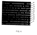
- FIG. 4 A longitudinal cross-section through a stack of 10 planes, generally indicated at 42-51, is illustrated in Fig. 4.
- the planes in this stack are separated in the Z direction by 3 micrometers, as noted above.
- Similar structures up to 30 planes thick, with data densities of 1.6 x 10 12 bits/cm 3 have been generated, with Fig. 5 showing a section from a 25-layer structure, having a density of 1.3 x 10 12 bits/cm 3 .
- a second order background subtraction has been digitally performed to remove the field ramp produced by the DIC imaging method.
- the optical memory formed by the foregoing process may be read by successively imaging each of the data-containing planes, such as planes 42-51, by directing laser light into the sample 10 carried by stage 11, again using the optics of the laser scanning microscope 22.
- the presence or absence of optically refractive beads, at specified X,Y and Z pixel locations in the sample can then be determined, so as to retrieve the data previously written.
- an Argon ion laser 50 (Fig. 1) directs a read beam 51 of light at a wavelength of 488 nm, for example, onto the specimen by way of dichroic mirror 21, the scanning mirrors of the laser confocal microscope 22, and the optics of the inverted microscope 12.
- the read beam 51 passes through the specimen and through lens 52 to a suitable light pipe 54 which directs the light to a photomultiplier light detector which forms a part of laser scanning microscope 22.
- the read beam scans each layer of the stack in the X-Y plane to produce a corresponding image, and by successively focusing the microscope 12 on the various planes by way of focus control 24, each layer of the stack can be read.
- the plane images so produced may be displayed on monitor 56 and may be supplied to suitable processing circuitry to determine the locations of those pixels which include data bits, for example in the form of refractory beads formed by the data writing process described above.
- these beams After passing through the sample, these beams are recombined so that they display an interference pattern in the image plane.
- Three-dimensional refractile data storage is entirely adaptable to the rotating disc format used in current commercial optical data storage products.
- a reading device requires incorporation of DIC transmission optics, and a recording (or writing) device requires a high peak power ultrafast modelocked laser source or other convenient short pulse source.
- resonance enhanced two photon absorbing media may provide much higher two-photon cross sections that could allow recording with a conventional laser diode.
Landscapes
- Engineering & Computer Science (AREA)
- Chemical & Material Sciences (AREA)
- Nanotechnology (AREA)
- Physics & Mathematics (AREA)
- Mathematical Physics (AREA)
- Theoretical Computer Science (AREA)
- Crystallography & Structural Chemistry (AREA)
- Optical Recording Or Reproduction (AREA)
- Microscoopes, Condenser (AREA)
- Holo Graphy (AREA)
- Testing, Inspecting, Measuring Of Stereoscopic Televisions And Televisions (AREA)
- Investigating Or Analysing Materials By Optical Means (AREA)
Applications Claiming Priority (3)
| Application Number | Priority Date | Filing Date | Title |
|---|---|---|---|
| US733030 | 1991-07-22 | ||
| US07/733,030 US5289407A (en) | 1991-07-22 | 1991-07-22 | Method for three dimensional optical data storage and retrieval |
| EP92916623A EP0595999B1 (de) | 1991-07-22 | 1992-07-22 | Verfahren zur dreidimensionalen optischen speicherung und wiedergabe von daten |
Related Parent Applications (1)
| Application Number | Title | Priority Date | Filing Date |
|---|---|---|---|
| EP92916623A Division EP0595999B1 (de) | 1991-07-22 | 1992-07-22 | Verfahren zur dreidimensionalen optischen speicherung und wiedergabe von daten |
Publications (1)
| Publication Number | Publication Date |
|---|---|
| EP0942431A2 true EP0942431A2 (de) | 1999-09-15 |
Family
ID=24945929
Family Applications (2)
| Application Number | Title | Priority Date | Filing Date |
|---|---|---|---|
| EP99109319A Withdrawn EP0942431A2 (de) | 1991-07-22 | 1992-07-22 | Verfahren zur dreidimensionalen optischen Speicherung und Wiedergabe von Daten |
| EP92916623A Expired - Lifetime EP0595999B1 (de) | 1991-07-22 | 1992-07-22 | Verfahren zur dreidimensionalen optischen speicherung und wiedergabe von daten |
Family Applications After (1)
| Application Number | Title | Priority Date | Filing Date |
|---|---|---|---|
| EP92916623A Expired - Lifetime EP0595999B1 (de) | 1991-07-22 | 1992-07-22 | Verfahren zur dreidimensionalen optischen speicherung und wiedergabe von daten |
Country Status (6)
| Country | Link |
|---|---|
| US (1) | US5289407A (de) |
| EP (2) | EP0942431A2 (de) |
| JP (1) | JP2810542B2 (de) |
| AT (1) | ATE187842T1 (de) |
| DE (1) | DE69230435T2 (de) |
| WO (1) | WO1993002454A1 (de) |
Cited By (1)
| Publication number | Priority date | Publication date | Assignee | Title |
|---|---|---|---|---|
| US8119041B2 (en) * | 2001-09-05 | 2012-02-21 | Fujifilm Corporation | Non-resonant two-photon absorption induction method and process for emitting light thereby |
Families Citing this family (111)
| Publication number | Priority date | Publication date | Assignee | Title |
|---|---|---|---|---|
| US6092728A (en) * | 1992-03-30 | 2000-07-25 | Symbol Technologies, Inc. | Miniature laser diode focusing module using micro-optics |
| US5900954A (en) * | 1992-06-01 | 1999-05-04 | Symbol Technologies, Inc. | Machine readable record carrier with hologram |
| US6871786B1 (en) | 1993-03-26 | 2005-03-29 | Symbol Technologies, Inc. | Method and apparatus for reading and writing indicia such as bar codes using a scanned laser |
| US5825402A (en) | 1993-03-26 | 1998-10-20 | Symbol Technologies, Inc. | Method and appratus for reading and writing indicia such as bar codes using a scanned laser beam |
| US5472759A (en) * | 1993-12-16 | 1995-12-05 | Martin Marietta Corporation | Optical volume memory |
| US5656186A (en) * | 1994-04-08 | 1997-08-12 | The Regents Of The University Of Michigan | Method for controlling configuration of laser induced breakdown and ablation |
| US7071477B2 (en) * | 1994-07-15 | 2006-07-04 | Baer Stephen C | Superresolution in microlithography and fluorescence microscopy |
| US6259104B1 (en) | 1994-07-15 | 2001-07-10 | Stephen C. Baer | Superresolution in optical microscopy and microlithography |
| US5952668A (en) * | 1994-07-15 | 1999-09-14 | Baer; Stephen C. | Resolution in microscopy and microlithography |
| US5866911A (en) * | 1994-07-15 | 1999-02-02 | Baer; Stephen C. | Method and apparatus for improving resolution in scanned optical system |
| US6903347B2 (en) | 1994-07-15 | 2005-06-07 | Stephen C. Baer | Superresolution in microlithography and fluorescence microscopy |
| US5923465A (en) * | 1994-10-28 | 1999-07-13 | Marc J. Byrd | System for scanning confocal image reconstruction from coherent recordings |
| US5559732A (en) * | 1994-12-27 | 1996-09-24 | Syracuse University | Branched photocycle optical memory device |
| US5592462A (en) * | 1994-12-30 | 1997-01-07 | Beldock; Donald T. | Three-dimensional optical data storage and retrieval |
| US5532998A (en) * | 1995-02-14 | 1996-07-02 | Serotech, Inc. | Optical spectroscopic information storage |
| CA2231114A1 (en) | 1995-09-06 | 1997-03-13 | The Research Foundation Of State University Of New York | Two-photon upconverting dyes and applications |
| WO1997011355A1 (en) * | 1995-09-19 | 1997-03-27 | Cornell Research Foundation, Inc. | Multi-photon laser microscopy |
| US5761111A (en) * | 1996-03-15 | 1998-06-02 | President And Fellows Of Harvard College | Method and apparatus providing 2-D/3-D optical information storage and retrieval in transparent materials |
| RU2172975C2 (ru) * | 1996-06-12 | 2001-08-27 | Оптиком АСА | Оптический логический элемент и оптическое логическое устройство |
| JP3198113B2 (ja) * | 1996-06-12 | 2001-08-13 | オプティコム エイエスエイ | 光論理素子および光論理機構 |
| US5936878A (en) * | 1997-01-06 | 1999-08-10 | Omd Devices Llc | Polymeric photo-chromic composition |
| US6316950B1 (en) | 1997-05-15 | 2001-11-13 | Lucent Technologies Inc. | Method and apparatus for imaging semiconductor devices |
| US6071748A (en) | 1997-07-16 | 2000-06-06 | Ljl Biosystems, Inc. | Light detection device |
| US6469311B1 (en) | 1997-07-16 | 2002-10-22 | Molecular Devices Corporation | Detection device for light transmitted from a sensed volume |
| US6825921B1 (en) | 1999-11-10 | 2004-11-30 | Molecular Devices Corporation | Multi-mode light detection system |
| US6982431B2 (en) * | 1998-08-31 | 2006-01-03 | Molecular Devices Corporation | Sample analysis systems |
| US6576476B1 (en) | 1998-09-02 | 2003-06-10 | Ljl Biosystems, Inc. | Chemiluminescence detection method and device |
| US6992761B2 (en) * | 1997-09-20 | 2006-01-31 | Molecular Devices Corporation | Broad range light detection system |
| US6297018B1 (en) | 1998-04-17 | 2001-10-02 | Ljl Biosystems, Inc. | Methods and apparatus for detecting nucleic acid polymorphisms |
| WO2000050877A1 (en) | 1999-02-23 | 2000-08-31 | Ljl Biosystems, Inc. | Frequency-domain light detection device |
| US6326605B1 (en) | 1998-02-20 | 2001-12-04 | Ljl Biosystems, Inc. | Broad range light detection system |
| US6132643A (en) * | 1998-01-06 | 2000-10-17 | Pavel; Eugen | Fluorescent photosensitive vitroceramics and process for the production thereof |
| AU744136B2 (en) | 1998-01-27 | 2002-02-14 | Wisconsin Alumni Research Foundation | Signal enhancement for fluorescence microscopy |
| US6020985A (en) * | 1998-01-30 | 2000-02-01 | Siros Technologies, Inc. | Multilayer reflection microhologram storage in tape media |
| US6212148B1 (en) | 1998-01-30 | 2001-04-03 | Siros Technologies, Inc. | Optical data storage by selective localized alteration of a format hologram |
| CA2326322C (en) * | 1998-04-21 | 2011-03-01 | University Of Connecticut | Free-form nanofabrication using multi-photon excitation |
| US5952131A (en) | 1998-04-27 | 1999-09-14 | Xerox Corporation | Core and shell matrix compositions and processes |
| US6147782A (en) * | 1998-05-01 | 2000-11-14 | Siros Technologies, Inc. | Positive unit magnification reflective optics for holographic storage |
| US6228787B1 (en) | 1998-07-27 | 2001-05-08 | Eugen Pavel | Fluorescent photosensitive glasses and process for the production thereof |
| AU5667599A (en) | 1998-07-27 | 2000-02-21 | Ljl Biosystems, Inc. | Apparatus and methods for time-resolved spectroscopic measurements |
| AU5223899A (en) | 1998-07-27 | 2000-02-21 | Ljl Biosystems, Inc. | Apparatus and methods for spectroscopic measurements |
| JP2000047046A (ja) * | 1998-07-31 | 2000-02-18 | Toshiyuki Watanabe | 屈折率分布型光学成形体の製造方法 |
| US6322933B1 (en) | 1999-01-12 | 2001-11-27 | Siros Technologies, Inc. | Volumetric track definition for data storage media used to record data by selective alteration of a format hologram |
| IL144870A0 (en) * | 1999-02-17 | 2002-06-30 | Univ Victoria | Erasable/rewritable optical data storage with photorefractive polymers |
| US7052812B1 (en) | 1999-04-12 | 2006-05-30 | The Regents Of The University Of California | Three-dimensional optical data storage in fluorescent dye-doped photopolymer |
| US6548796B1 (en) * | 1999-06-23 | 2003-04-15 | Regents Of The University Of Minnesota | Confocal macroscope |
| DE19932902A1 (de) | 1999-07-12 | 2001-01-25 | Beiersdorf Ag | Datenspeicher |
| DE19935776A1 (de) * | 1999-07-26 | 2001-02-08 | Beiersdorf Ag | Datenspeicher |
| DE19935775A1 (de) | 1999-07-26 | 2001-02-08 | Beiersdorf Ag | Datenspeicher und Verfahren zum Schreiben von Information in einen Datenspeicher |
| US6573026B1 (en) | 1999-07-29 | 2003-06-03 | Corning Incorporated | Femtosecond laser writing of glass, including borosilicate, sulfide, and lead glasses |
| US6310850B1 (en) | 1999-07-29 | 2001-10-30 | Siros Technologies, Inc. | Method and apparatus for optical data storage and/or retrieval by selective alteration of a holographic storage medium |
| US6512606B1 (en) | 1999-07-29 | 2003-01-28 | Siros Technologies, Inc. | Optical storage media and method for optical data storage via local changes in reflectivity of a format grating |
| EP1204977A4 (de) * | 1999-07-29 | 2003-08-13 | Corning Inc | Direktes schreiben optischer vorrichtungen aus siliziumbasiertem glas unter verwendung von femtosekundenlaserimpulsen |
| US6977137B2 (en) | 1999-07-29 | 2005-12-20 | Corning Incorporated | Direct writing of optical devices in silica-based glass using femtosecond pulse lasers |
| US6322931B1 (en) | 1999-07-29 | 2001-11-27 | Siros Technologies, Inc. | Method and apparatus for optical data storage using non-linear heating by excited state absorption for the alteration of pre-formatted holographic gratings |
| IL131575A (en) | 1999-08-24 | 2003-11-23 | U C Laser Ltd | Volume holograms in transparent materials |
| US6796148B1 (en) | 1999-09-30 | 2004-09-28 | Corning Incorporated | Deep UV laser internally induced densification in silica glasses |
| US7167615B1 (en) | 1999-11-05 | 2007-01-23 | Board Of Regents, The University Of Texas System | Resonant waveguide-grating filters and sensors and methods for making and using same |
| DE10008328A1 (de) * | 2000-02-23 | 2002-01-31 | Tesa Ag | Datenspeicher |
| US6341009B1 (en) | 2000-02-24 | 2002-01-22 | Quantronix Corporation | Laser delivery system and method for photolithographic mask repair |
| WO2001067176A1 (en) | 2000-03-09 | 2001-09-13 | Xerox Corporation | Three dimensional optical memory storage |
| US6624915B1 (en) * | 2000-03-16 | 2003-09-23 | Science Applications International Corporation | Holographic recording and micro/nanofabrication via ultrafast holographic two-photon induced photopolymerization (H-TPIP) |
| EP1598699A3 (de) | 2000-05-23 | 2009-05-20 | Aprilis, Inc. | Datenspeichermedium das ein kolloidales Metall enthält und Verfahren zur Herstellung |
| DE10028113A1 (de) * | 2000-06-07 | 2001-12-20 | Beiersdorf Ag | Datenspeicher |
| ATE440305T1 (de) * | 2000-06-15 | 2009-09-15 | 3M Innovative Properties Co | Erzeugung eines mehrfarbenbildes mittels eines multiphoton photochemischen verfahren |
| WO2001096917A2 (en) * | 2000-06-15 | 2001-12-20 | 3M Innovative Properties Company | Multiphoton curing to provide encapsulated optical elements |
| JP2004503831A (ja) * | 2000-06-15 | 2004-02-05 | スリーエム イノベイティブ プロパティズ カンパニー | マルチパス多光子吸収方法および装置 |
| KR100795759B1 (ko) * | 2000-06-15 | 2008-01-21 | 쓰리엠 이노베이티브 프로퍼티즈 캄파니 | 미세유체 물품의 제조 방법 |
| US6852766B1 (en) * | 2000-06-15 | 2005-02-08 | 3M Innovative Properties Company | Multiphoton photosensitization system |
| WO2001096959A2 (en) * | 2000-06-15 | 2001-12-20 | 3M Innovative Properties Company | Multidirectional photoreactive absorption method |
| JP4965052B2 (ja) * | 2000-06-15 | 2012-07-04 | スリーエム イノベイティブ プロパティズ カンパニー | 3次元光学素子の加工方法 |
| US6687000B1 (en) | 2000-06-26 | 2004-02-03 | Wisconsin Alumni Research Foundation | Photon-sorting spectroscopic microscope system |
| DE10039370A1 (de) * | 2000-08-11 | 2002-02-28 | Eml Europ Media Lab Gmbh | Holographischer Datenspeicher |
| DE10039372C2 (de) | 2000-08-11 | 2003-05-15 | Tesa Scribos Gmbh | Holographischer Datenspeicher |
| DE10039374A1 (de) * | 2000-08-11 | 2002-02-21 | Eml Europ Media Lab Gmbh | Holographischer Datenspeicher |
| US6884961B1 (en) | 2000-08-24 | 2005-04-26 | Uc Laser Ltd. | Intravolume diffractive optical elements |
| DE10060235A1 (de) * | 2000-12-05 | 2002-06-13 | Tesa Ag | Verwendung eines Packbands als holographischer Datenträger |
| AUPR197400A0 (en) * | 2000-12-08 | 2001-01-11 | Swinburne University Of Technology | Data storage |
| US6999397B2 (en) * | 2001-03-23 | 2006-02-14 | Daewoo Electronics Corp. | Holographic digital data storage system compatible with holographic and reflective medium |
| DE10116060B4 (de) * | 2001-03-30 | 2005-01-13 | Tesa Scribos Gmbh | Lithograph mit Triggermaske und Verfahren zum Herstellen digitaler Hologramme in einem Speichermedium |
| DE10116058B4 (de) * | 2001-03-30 | 2006-05-11 | Tesa Scribos Gmbh | Verfahren zum Herstellen digitaler Hologramme in einem Speichermedium und Lithograph zum Herstellen digitaler Hologramme in einem Speichermedium |
| EP1377880B1 (de) * | 2001-04-12 | 2005-06-01 | tesa scribos GmbH | Lithograph und mikroskop mit eindimensionaler triggermaske und verfahren zum herstellen digitaler hologramme in einem speichermedium |
| US20040012872A1 (en) * | 2001-06-14 | 2004-01-22 | Fleming Patrick R | Multiphoton absorption method using patterned light |
| DE10128901A1 (de) * | 2001-06-15 | 2002-12-19 | Tesa Ag | Verfahren zum Eingeben von Information in einen optisch beschreibbaren und auslesbaren Datenspeicher |
| DE10128902A1 (de) * | 2001-06-15 | 2003-10-16 | Tesa Scribos Gmbh | Holographischer Datenspeicher |
| EP1406890A4 (de) * | 2001-07-13 | 2004-11-24 | Trustees Boston College | Phthalidverbindungen, die sich für optische aufnahmen eignen |
| US7001708B1 (en) | 2001-11-28 | 2006-02-21 | University Of Central Florida Research Foundation, Inc. | Photosensitive polymeric material for worm optical data storage with two-photon fluorescent readout |
| US7072275B2 (en) * | 2001-12-04 | 2006-07-04 | Landauer, Incorporated | Optical single-bit recording and fluorescent readout utilizing aluminum oxide single crystals |
| AU2002360466A1 (en) * | 2001-12-04 | 2003-06-17 | Landauer, Inc. | Aluminum oxide material for optical data storage |
| US6950591B2 (en) * | 2002-05-16 | 2005-09-27 | Corning Incorporated | Laser-written cladding for waveguide formations in glass |
| EP2221810B1 (de) | 2002-10-10 | 2014-09-24 | Landauer, Inc. | Verfahren zur Löschung der Informationen aufgezeichnet auf ein lumineszierendes Datenspeichermedium enthaltend ein Material auf Basis von Aluminiumoxid |
| CA2497759C (en) | 2002-10-10 | 2013-08-20 | Landauer, Inc. | Bit-wise optical data storage utilizing aluminum oxide single crystal medium |
| US7285363B2 (en) * | 2002-11-08 | 2007-10-23 | The University Of Connecticut | Photoactivators, methods of use, and the articles derived therefrom |
| US20030155667A1 (en) * | 2002-12-12 | 2003-08-21 | Devoe Robert J | Method for making or adding structures to an article |
| EP1616216B1 (de) * | 2003-04-13 | 2018-11-07 | Max-Planck-Gesellschaft zur Förderung der Wissenschaften e.V. | Räumlich hochauflösendes abbilden |
| WO2005064603A1 (ja) * | 2003-12-16 | 2005-07-14 | Matsushita Electric Industrial Co., Ltd. | 光ディスク装置及び光ディスク |
| DE102005040671B4 (de) * | 2005-08-26 | 2008-04-30 | MAX-PLANCK-Gesellschaft zur Förderung der Wissenschaften e.V. | Verfahren und Vorrichtungen zum Speichern einer dreidimensionalen Anordnung von Datenbits in einem Festkörper |
| US7964333B1 (en) | 2006-06-09 | 2011-06-21 | University Of Central Florida Research Foundation, Inc. | FRET-based two photon three dimensional optical data storage |
| WO2009126888A2 (en) | 2008-04-10 | 2009-10-15 | Services Petroliers Schlumberger | Method for characterizing a geological formation traversed by a borehole |
| US8725477B2 (en) * | 2008-04-10 | 2014-05-13 | Schlumberger Technology Corporation | Method to generate numerical pseudocores using borehole images, digital rock samples, and multi-point statistics |
| US7902525B2 (en) * | 2008-10-24 | 2011-03-08 | Landauer, Inc. | Method of luminescent solid state dosimetry of mixed radiations |
| US8311788B2 (en) * | 2009-07-01 | 2012-11-13 | Schlumberger Technology Corporation | Method to quantify discrete pore shapes, volumes, and surface areas using confocal profilometry |
| US20110004447A1 (en) * | 2009-07-01 | 2011-01-06 | Schlumberger Technology Corporation | Method to build 3D digital models of porous media using transmitted laser scanning confocal mircoscopy and multi-point statistics |
| FR2961816B1 (fr) | 2010-06-25 | 2012-07-06 | Coatex Sas | Emulsions acryliques alkali gonflables sans tensio-actif, leur utilisation dans des formulations aqueuses et formulations les contenant. |
| FR2961815B1 (fr) | 2010-06-25 | 2013-05-10 | Coatex Sas | Emulsions acryliques alkali gonflables a l'acide acrylique, leur utilisation dans des formulations aqueuses et formulations les contenant. |
| FR2972370B1 (fr) | 2011-03-07 | 2013-03-01 | Coatex Sas | Procede d'epaississement d'une formulation cosmetique a partir d'une emulsion alkali gonflable d'un polymere a l'amps et riche en acide acrylique. |
| US9664614B2 (en) | 2011-07-11 | 2017-05-30 | University Of Limerick | Method for high resolution sum-frequency generation and infrared microscopy |
| EP2941662B1 (de) | 2013-01-04 | 2019-03-13 | University of Limerick | Differential-infrarot-nanoskopiesystem und -verfahren |
| US10970363B2 (en) | 2017-10-17 | 2021-04-06 | Microsoft Technology Licensing, Llc | Machine-learning optimization of data reading and writing |
| US11335373B1 (en) | 2021-02-22 | 2022-05-17 | Seagate Technology Llc | Plasmonic transducer head for writing data to and reading data from an optical recording medium ultilizing a fluorescent dye |
| US20240209226A1 (en) | 2022-12-23 | 2024-06-27 | Dupont Electronics, Inc. | Aqueous inkjet compositions including polymeric thickener |
Family Cites Families (21)
| Publication number | Priority date | Publication date | Assignee | Title |
|---|---|---|---|---|
| US3013467A (en) * | 1957-11-07 | 1961-12-19 | Minsky Marvin | Microscopy apparatus |
| US4041476A (en) * | 1971-07-23 | 1977-08-09 | Wyn Kelly Swainson | Method, medium and apparatus for producing three-dimensional figure product |
| US3508208A (en) * | 1967-12-27 | 1970-04-21 | Bell Telephone Labor Inc | Optical organic memory device |
| US3999009A (en) * | 1971-03-11 | 1976-12-21 | U.S. Philips Corporation | Apparatus for playing a transparent optically encoded multilayer information carrying disc |
| US3855426A (en) * | 1971-03-11 | 1974-12-17 | Philips Corp | Video disc recording and optical playback system therefor |
| US3848095A (en) * | 1972-12-20 | 1974-11-12 | I O Metrics Corp | Three dimensional electro-optical retrieval system |
| US3946367A (en) * | 1972-12-20 | 1976-03-23 | Videonics Of Hawaii, Inc. | Three dimensional electro-optical retrieval system |
| NL7402012A (nl) * | 1974-02-14 | 1975-08-18 | Philips Nv | Registratiedrager waarop informatie is aange- bracht in een optisch uitleesbare struktuur. |
| US4219704A (en) * | 1974-10-21 | 1980-08-26 | Eli S. Jacobs | Record playback apparatus for optical data records |
| US4090031A (en) * | 1974-10-21 | 1978-05-16 | Eli S. Jacobs | Multi-layered opitcal data records and playback apparatus |
| US4163600A (en) * | 1974-10-21 | 1979-08-07 | Eli S. Jacobs | Light beam scanner |
| US4333165A (en) * | 1975-01-27 | 1982-06-01 | Formigraphic Engine Corporation | Three-dimensional pattern making methods |
| US4078229A (en) * | 1975-01-27 | 1978-03-07 | Swanson Wyn K | Three dimensional systems |
| US4466080A (en) * | 1975-01-27 | 1984-08-14 | Formigraphic Engine Corporation | Three-dimensional patterned media |
| US4288861A (en) * | 1977-12-01 | 1981-09-08 | Formigraphic Engine Corporation | Three-dimensional systems |
| US4471470A (en) * | 1977-12-01 | 1984-09-11 | Formigraphic Engine Corporation | Method and media for accessing data in three dimensions |
| US4288862A (en) * | 1977-12-21 | 1981-09-08 | Nippon Telegraph And Telephone Public Corp. | Memory circuit |
| NL7803069A (nl) * | 1978-03-22 | 1979-09-25 | Philips Nv | Meerlaags informatieschijf. |
| JPH0654547B2 (ja) * | 1984-10-08 | 1994-07-20 | 日本電気株式会社 | 光ピツクアツプ |
| US5034613A (en) * | 1989-11-14 | 1991-07-23 | Cornell Research Foundation, Inc. | Two-photon laser microscopy |
| JP2769393B2 (ja) * | 1991-04-26 | 1998-06-25 | 直弘 丹野 | 立体光記録装置 |
-
1991
- 1991-07-22 US US07/733,030 patent/US5289407A/en not_active Expired - Fee Related
-
1992
- 1992-07-22 EP EP99109319A patent/EP0942431A2/de not_active Withdrawn
- 1992-07-22 EP EP92916623A patent/EP0595999B1/de not_active Expired - Lifetime
- 1992-07-22 AT AT92916623T patent/ATE187842T1/de not_active IP Right Cessation
- 1992-07-22 DE DE69230435T patent/DE69230435T2/de not_active Expired - Fee Related
- 1992-07-22 WO PCT/US1992/005858 patent/WO1993002454A1/en not_active Ceased
- 1992-07-22 JP JP5502893A patent/JP2810542B2/ja not_active Expired - Lifetime
Cited By (1)
| Publication number | Priority date | Publication date | Assignee | Title |
|---|---|---|---|---|
| US8119041B2 (en) * | 2001-09-05 | 2012-02-21 | Fujifilm Corporation | Non-resonant two-photon absorption induction method and process for emitting light thereby |
Also Published As
| Publication number | Publication date |
|---|---|
| EP0595999B1 (de) | 1999-12-15 |
| JP2810542B2 (ja) | 1998-10-15 |
| ATE187842T1 (de) | 2000-01-15 |
| US5289407A (en) | 1994-02-22 |
| JPH07501168A (ja) | 1995-02-02 |
| DE69230435T2 (de) | 2000-05-11 |
| WO1993002454A1 (en) | 1993-02-04 |
| DE69230435D1 (de) | 2000-01-20 |
| EP0595999A1 (de) | 1994-05-11 |
| EP0595999A4 (en) | 1994-09-14 |
Similar Documents
| Publication | Publication Date | Title |
|---|---|---|
| US5289407A (en) | Method for three dimensional optical data storage and retrieval | |
| Strickler et al. | Three-dimensional optical data storage in refractive media by two-photon point excitation | |
| US5034613A (en) | Two-photon laser microscopy | |
| Strickler et al. | Two-photon excitation in laser scanning fluorescence microscopy | |
| US6483735B1 (en) | Two-photon, three-or four-dimensional, color radiation memory | |
| US6867408B1 (en) | Erasable/rewritable optical data storage with photorefractive polymers | |
| JPH0628672A (ja) | 光学的データ記憶体並びにこの記録装置及び記録再生装置 | |
| EP1576591B1 (de) | Bitweise optische datenspeicherung mit einem einkristalligen aluminiumoxidmedium | |
| CA2300982A1 (en) | Three-dimensional optical memory with fluorescent photosensitive material | |
| Akselrod et al. | Bit-wise volumetric optical memory utilizing two-photon absorption in aluminum oxide medium | |
| Kawata | Photorefractive optics in three-dimensional digital memory | |
| WILSON | Confocal Microscopy: Basic Principles | |
| US7190649B2 (en) | Bit-wise optical data storage utilizing aluminum oxide single crystal medium | |
| US6205106B1 (en) | Memory card recording/reproducing with two light sources and a light value matrix | |
| Strickler et al. | Signal measurements of multilayer refractive write-once data storage media | |
| Brand et al. | Super-resolution in optical data storage | |
| JP4820400B2 (ja) | 酸化アルミニウム単結晶媒体を利用するビット方式光学データ記憶 | |
| Kawata et al. | 3D data storage and near-field recording | |
| Kawata | Three-Dimensional Optical Data Storage with a Multi-layered Recording Medium |
Legal Events
| Date | Code | Title | Description |
|---|---|---|---|
| PUAI | Public reference made under article 153(3) epc to a published international application that has entered the european phase |
Free format text: ORIGINAL CODE: 0009012 |
|
| AC | Divisional application: reference to earlier application |
Ref document number: 595999 Country of ref document: EP |
|
| AK | Designated contracting states |
Kind code of ref document: A2 Designated state(s): DE FR GB NL |
|
| STAA | Information on the status of an ep patent application or granted ep patent |
Free format text: STATUS: THE APPLICATION IS DEEMED TO BE WITHDRAWN |
|
| 18D | Application deemed to be withdrawn |
Effective date: 20020306 |