EP0942462B1 - Méthode et structure en vue de protéger une zone voisine d'une zone à graver, et méthode de formation d'un fusible - Google Patents
Méthode et structure en vue de protéger une zone voisine d'une zone à graver, et méthode de formation d'un fusible Download PDFInfo
- Publication number
- EP0942462B1 EP0942462B1 EP99103818A EP99103818A EP0942462B1 EP 0942462 B1 EP0942462 B1 EP 0942462B1 EP 99103818 A EP99103818 A EP 99103818A EP 99103818 A EP99103818 A EP 99103818A EP 0942462 B1 EP0942462 B1 EP 0942462B1
- Authority
- EP
- European Patent Office
- Prior art keywords
- etch
- guard cell
- area
- layer
- well
- Prior art date
- Legal status (The legal status is an assumption and is not a legal conclusion. Google has not performed a legal analysis and makes no representation as to the accuracy of the status listed.)
- Expired - Lifetime
Links
Images




Classifications
-
- H—ELECTRICITY
- H10—SEMICONDUCTOR DEVICES; ELECTRIC SOLID-STATE DEVICES NOT OTHERWISE PROVIDED FOR
- H10P—GENERIC PROCESSES OR APPARATUS FOR THE MANUFACTURE OR TREATMENT OF DEVICES COVERED BY CLASS H10
- H10P50/00—Etching of wafers, substrates or parts of devices
- H10P50/73—Etching of wafers, substrates or parts of devices using masks for insulating materials
-
- H—ELECTRICITY
- H10—SEMICONDUCTOR DEVICES; ELECTRIC SOLID-STATE DEVICES NOT OTHERWISE PROVIDED FOR
- H10P—GENERIC PROCESSES OR APPARATUS FOR THE MANUFACTURE OR TREATMENT OF DEVICES COVERED BY CLASS H10
- H10P50/00—Etching of wafers, substrates or parts of devices
- H10P50/20—Dry etching; Plasma etching; Reactive-ion etching
- H10P50/28—Dry etching; Plasma etching; Reactive-ion etching of insulating materials
- H10P50/282—Dry etching; Plasma etching; Reactive-ion etching of insulating materials of inorganic materials
- H10P50/283—Dry etching; Plasma etching; Reactive-ion etching of insulating materials of inorganic materials by chemical means
-
- H—ELECTRICITY
- H10—SEMICONDUCTOR DEVICES; ELECTRIC SOLID-STATE DEVICES NOT OTHERWISE PROVIDED FOR
- H10W—GENERIC PACKAGES, INTERCONNECTIONS, CONNECTORS OR OTHER CONSTRUCTIONAL DETAILS OF DEVICES COVERED BY CLASS H10
- H10W20/00—Interconnections in chips, wafers or substrates
- H10W20/01—Manufacture or treatment
- H10W20/071—Manufacture or treatment of dielectric parts thereof
- H10W20/081—Manufacture or treatment of dielectric parts thereof by forming openings in the dielectric parts
-
- H—ELECTRICITY
- H10—SEMICONDUCTOR DEVICES; ELECTRIC SOLID-STATE DEVICES NOT OTHERWISE PROVIDED FOR
- H10W—GENERIC PACKAGES, INTERCONNECTIONS, CONNECTORS OR OTHER CONSTRUCTIONAL DETAILS OF DEVICES COVERED BY CLASS H10
- H10W20/00—Interconnections in chips, wafers or substrates
- H10W20/40—Interconnections external to wafers or substrates, e.g. back-end-of-line [BEOL] metallisations or vias connecting to gate electrodes
- H10W20/49—Adaptable interconnections, e.g. fuses or antifuses
- H10W20/493—Fuses, i.e. interconnections changeable from conductive to non-conductive
Definitions
- the present invention relates to the fabrication of semiconductor devices. More particularly, the present invention relates to the fabrication of a guard cell that advantageously separates and protects one structure of the semiconductor device from other neighboring structures.
- microcavities and their fabrication are known in the art. They are formed in conjunction with semiconductor devices such as electrically blowable fuses.
- the fuse portion is typically formed of a material that changes its state from conductive to non-conductive when a current exceeding a predefined threshold is passed through. This change in state sometimes produces particulate material.
- the fuse portion is typically disposed in a dielectric microcavity, i.e., a sealed, hollow chamber in a dielectric layer.
- any particulate material that may be formed when fuse portion is blown is kept contained with microcavity, thereby minimizing or essentially eliminating any possibility of particulate contamination of the IC surface.
- the microcavity itself is typically formed in a multistep process.
- FIGs. 1A through I C illustrate a prior art process for forming a microcavity in the context of an electrically blown fuse.
- a fuse portion 102 is shown disposed on a substrate 104.
- Fuse portion 102 typically comprises a conductor made of a suitable fuse material such as doped polysilicon or metal.
- the fuse portion is also sometimes capped with a silicon nitride layer 103.
- another oxide layer 106 is deposited.
- a silicon nitride layer 108 is then deposited above oxide layer 106.
- a photoresist layer 110 is deposited and patterned to form an opening 112. Patterned photoresist mask 110 is then employed to etch through silicon nitride layer 108 to expose a portion of oxide layer 106 above fuse portion 102. Although a patterned photoresist mask is shown here, other methods can be used to etch through silicon nitride layer 108 and expose a portion of the oxide layer 106.
- a subsequent isotropic etch is performed to create the microcavity.
- the microcavity etch preferably employs an etch process that is selective both to the liner material of fuse portion 102 and silicon nitride layer 108. As is apparent, with such a process silicon nitride layer 108 acts as a hard mask during the isotropic etch.
- microcavity 114 has been isotropically etched out of oxide layer 106 through the opening in silicon nitride layer 108. Subsequent to the formation of microcavity 114, the opening in silicon nitride layer 108 is sealed with plug material 116 while microcavity 114 is left hollow, thereby sealing fuse portion 102 within microcavity 114.
- the degree to which the etch extends into oxide layer 106 is difficult to control.
- structures 118 which neighbor the fuse may be affected by the etch, as depicted in Fig. 1C, possibly resulting in the neighboring structures being damaged or made inoperative.
- the process may include accurately timing and halting the etch duration. This requires close monitoring of the etch process and is subject to error.
- neighboring structures typically are located a distance from the fuse determined to be sufficient to avoid affecting those structures with the etch. Such distances may be determined from, among other factors, the characteristic interactions of the etch process and material being etched, such as the etch rate.
- Spacings used must be large enough to take into account the unpredictability of the process and possible errors in efforts to control the process.
- the requirement of such conservative spacings effectively limit the density with which devices can be formed on the IC, thereby limiting the number of devices that can be included on the IC.
- the invention relates, in one embodiment, to a method for protecting neighboring area that is adjacent to a first area to be etched on a substrate.
- the method includes creating a well substantially surrounding the first area, the neighboring area being disposed outside the well.
- the method also includes filling the well with a material that is substantially selective to an etch that is subsequently employed to etch the first area, thereby forming a guard cell.
- the invention in yet another embodiment, relates to a method for protecting a first area from an etch process configured to etch a neighboring area that is adjacent to the first area on a substrate.
- the method includes creating a well substantially surrounding the first area, the neighboring area being disposed outside the well.
- the method also includes filling the well with a material that is substantially selective to the etch that is subsequently employed to etch the neighboring area, thereby forming a guard cell.
- the integrated circuit is, for example, a memory IC such as a random access memory (RAM), a dynamic random access memory (DRAM), or a synchronous DRAM (SDRAM).
- the integrated circuit may also include other types of circuits such as an application specific IC (ASIC), a merged DRAM-logic circuit (embedded DRAM), or any other logic circuit.
- ASIC application specific IC
- merged DRAM-logic circuit embedded DRAM
- numerous integrated circuits are formed on the wafer in parallel. After processing is finish, the wafer is diced to separate the integrated circuits to individual chips. The chips are then packaged, resulting in a final product that is used in, for example, consumer products such as computer systems, cellular phones, personal digital assistants (PDAs), and other electronic products.
- PDAs personal digital assistants
- One embodiment of the present invention advantageously provides a guard cell before etching of the microcavity.
- the guard cell limits the area which is etched to form the microcavity, allowing neighboring structures to be packed more densely without risking damage to the neighboring structures from the microcavity etching process. In this manner, integrated circuits can be formed with higher densities and thus more devices.
- Fig. 2 illustrates a cross-sectional view of a fuse portion 202 formed above a substrate of the integrated circuit.
- a substrate 204 or portions thereof may be formed of various materials used in the fabrication of the integrated circuit, for example silicon or an oxide layer overlying silicon.
- a fuse portion 202 may be formed of any suitable fuse material known in the art, for example polysilicon, tungsten silicide, copper, or tungsten.
- Fig. 3 further illustrates the formation of a dielectric layer 302 over fuse portion 202 and substrate 204.
- Dielectric layer 302 may be formed of any suitable dielectric material, such as an oxide, combination of oxides, borophosphosilicate glass, or tetraethylorthosilicate (TEOS).
- a well 402 is formed in dielectric layer 302 around fuse portion 202.
- Well 402 can be formed by any suitable process known to those who are skilled in the art such as an anisotropic dry etch.
- well 402 preferably extends from the surface of dielectric layer 302 to the surface of substrate 204.
- well 402 in the areas of well 402 that are closest to fuse portion 202 (not shown), well 402 preferably extends from the surface of dielectric layer 302 to the surface of the gate (not shown) extending from fuse portion 202.
- well 402 is located some distance from fuse portion 202.
- the distance between fuse portion 202 and well 402 is determined, in part, by the desired size of the microcavity and the density requirement of the IC. For example, the distance between the well and the side of fuse portion 202 may be less than 2 microns.
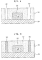
- well 402 is filled to form a guard cell 502.
- Guard cell 502, shown in Fig. 5, may be formed with any suitable material that is substantially selective to the subsequent guard cell 502 is preferably a material that does not allow the thickness of guard cell 502 to be etched through during the subsequent etch process employed to form the microcavity.
- guard cell 502 The selection of the appropriate material depends, in part, on the nature of the subsequent microcavity etch process as well as the thickness of the guard cell layer (which depends, in part, on the design rules employed). Note that it is not necessary that the material of guard cell 502 be absolutely unetched during this subsequent etch process. By way of example, materials such as nitride, tungsten, or polysilicon may be employed for guard cell 502.
- Fig. 6 illustrates the process continuing with the formation of a capping layer 602 overlying dielectric layer 302 and guard cell 502.
- Layer 602 may be formed of any suitable material that is substantially selective to the etch process subsequently used for the formation of the microcavity surrounding fuse portion 202. That is, the material of capping layer 602 is preferably a material that does not allow the thickness of capping layer 602 to be etched through during the subsequent etch process employed to form the microcavity. The selection of the appropriate material depends, in part, on the nature of the subsequent microcavity etch process as well as the thickness of capping layer 602 (which depends, in part, on the design rules employed). Note that it is not necessary that the material of capping layer 602 be absolutely unetched during this subsequent etch process. By way of example, materials such as nitride, tungsten, or polysilicon may be employed for capping layer 602.
- An access hole 702 is formed in layer 602 within the boundaries of guard cell 502.
- Access hole 702 may be formed through layer 602 by any suitable method known to those skilled in the art, such as applying a mask over layer 602 and performing a wet or dry etch using that mask.
- Fig. 7B depicts the result of an isotropic etch performed through access hole 702 to form microcavity 704 within guard cell 502 and around fuse portion 202.
- the etch process used to form microcavity 704 may be any isotropic etch selective to the materials used to form substrate 204, fuse portion 202, guard cell 502 and layer 602.
- etching of material outside guard cell 502 including material of dielectric layer 302.
- plug material 706 is used to fill access hole 702 to enclosed microcavity 704. Any process and material known to those skilled in the art may be used to plug access hole 702 without substantially extending into microcavity 704.
- access hole 702 may be plugged by a plasma TEOS deposition process.
- Fig. 8A further illustrates the embodiment of the present invention shown in Fig. 7C, from a top-down view of a cross-section taken along the line B - B' of Fig. 7C.
- Figs. 7A through 7C are front views of the cross-section taken along the line C - C' shown in Fig. 8A.
- guard cell 502 substantially surrounds fuse portion 202, which is a portion of a gate 802.
- guard cell 502 creates a physical boundary between microcavity 704 that is around fuse portion 202, and the remaining portions of dielectric layer 302.
- guard cell 502 substantially surrounds fuse portion 202
- Fig. 8B depicts guard cell 502, gate 802 including fuse portion 202, and microcavity 704 overlying substrate 204.
- Remaining dielectric layer 302 lies outside guard cell 502, while other layers (not shown) overlie each of the above named elements.
- fuse portion 202 is a portion of gate 802, and microcavity 704 is desired only around fuse portion 202, gate 802 extends beyond fuse portion 202 through, essentially, guard cell 502.
- the etch is performed substantially to the surface of gate 802 in those areas where gate 802 extends through guard cell 502.
- guard cell 502 One result of forming guard cell 502 is that fuse portion 202 is substantially surrounded by microcavity 704, and microcavity 704 is substantially physically isolated from the remaining dielectric layer 302. Accordingly, neighboring devices can be positioned as close to guard cell 502 as desired, without risking damage to the neighboring devices, and without requiring a high level of monitoring the microcavity etch process. Thus, the devices on the IC can be more densely packed.
- a material that is not selective to the isotropic etch process used to formed microcavity 704 may be disposed between fuse portion 202 and substrate 204.
- Fig. 7D shows this embodiment wherein a depression or trench 750 is formed in substrate 204 prior to the deposition of dielectric material 302. In this manner, dielectric material 302 is present above and below fuse portion 202. During the isotropic etch process, this dielectric material is removed from both above and below fuse portion 202, thereby forming a cavity or void not only above but also below the fuse portion itself.
- Fig. 8B is a top view illustration of this embodiment after isotropic etching is completed.
- the cavity may be formed only below fuse portion 202 if desired by depositing the dielectric material to be etched only below fuse portion 202. It should also be recognized that the cavity may be formed on only one side or both sides (with or without cavities above and/or below the fuse portion) of fuse portion 202 by depositing the dielectric material only in the region where formation of the cavity is desired. Again, it should also be emphasized that although fuse portion 202 is shown herein for ease of discussion, any structure may be protected by the guard cell of the present invention.
- the process 900 used to form a fuse is depicted in the flow chart of Fig. 9.
- a fuse portion is provided on a substrate with an oxide layer overlying both the fuse portion and substrate.
- a well is formed in the oxide layer in step 904, such that the well is around the fuse portion.
- the well formed in step 904 is then filled with guard cell material in step 906 to form a guard cell substantially surrounding the fuse portion.
- the guard cell material is any suitable material that is selective to an isotropic etch that will be performed subsequently in process 900.
- a selective layer is formed in step 908 over the oxide layer and the guard cell of material that is also selected to the isotropic etch performed subsequently in process 900.
- an access hole is formed through the selective layer to expose the portion of the oxide layer that overlies the fused portion and lies within the guard cell boundaries.
- an isotropic etch is performed to form the microcavity around the fused portion and within the guard cell in step 912.
- the access hole in the selective layer is filled in step 914, thereby sealing the microcavity formed in step 912.
- guard cell may be employed to protect neighboring areas and neighboring devices from the isotropic etch process employed to form the cavity within the guard cell
- the guard cell it is also possible to employ the guard cell to protect the area and/or devices within the guard cell while etching takes place outside the guard cell.
- an etch process may be employed to remove portions of layer 602 outside of guard cell 502. In this manner, the area within the guard cell would be protected from any subsequent etch process that is substantially selective to the materials of capping layer 602 and of guard cell 502.
Landscapes
- Design And Manufacture Of Integrated Circuits (AREA)
- Fuses (AREA)
- Drying Of Semiconductors (AREA)
- Internal Circuitry In Semiconductor Integrated Circuit Devices (AREA)
Claims (19)
- Procédé de gravure isotrope d'une première zone dans une couche (302) chevauchant un substrat (204), protégeant ainsi la zone voisine adjacente à la première zone qui doit être gravée de manière isotrope, le procédé comprenant :la création d'une cellule de protection (502) entourant la première zone, la zone voisine étant disposée à l'extérieur de la cellule de protection 502), la cellule de protection étant composée d'un matériau de cellule de protection sensiblement sélectif à une gravure isotrope utilisée pour graver la première zone ; etensuite, la réalisation de la gravure isotrope dans la première zone, la cellule de protection (502) empêchant la gravure isotrope de graver la zone voisine à l'extérieur de la cellule de protection.
- Procédé selon la revendication 1,
dans lequel la création de la cellule de protection (502) comprend en outre :la formation de la couche (302) chevauchant le substrat pour obtenir une couche diélectrique ; la formation d'un puits (402) dans la couche diélectrique (302), le puits entourant sensiblement la première zone ; etle remplissage du puits (402) avec le matériau de cellule de protection. - Procédé selon la revendication 1,
comprenant en outre : la formation d'une porte (802) chevauchant le substrat (204), la porte (802) incluant une partie de fusible (202), la cellule de protection (502) étant formée en entourant sensiblement la partie de fusible (202). - Procédé selon la revendication 3,
dans lequel le matériau diélectrique (302) est disposé au-dessus et au-dessous de la porte (802). - Procédé selon la revendication 1,
dans lequel le matériau de cellule de protection est choisi dans le groupe composé de tungstène, polysilicium, et nitrure de silicium. - Procédé selon la revendication 1,
dans lequel la gravure isotrope est une gravure humide HF de finition. - Procédé selon la revendication 3,
comprenant en outre, avant la gravure :la formation d'une couche de surfaçage (602) chevauchant la porte (802) et la cellule de protection (502), la couche de surfaçage (602) étant composée d'un matériau sensiblement sélectif à la gravure isotrope utilisée pour graver ensuite une microcavité à l'intérieur de la cellule de protection (502) ;la création d'un trou d'accès (702) à travers la couche de surfaçage (602) au-dessus de la première zone autour de la porte qui est délimitée par la cellule de protection (502) ; etla gravure de la microcavité autour de la porte (802) et à l'intérieur de la première zone délimitée par la cellule de protection avec la gravure isotrope. - Procédé selon la revendication 7,
dans lequel la cellule de protection (502) n'est pas gravée complètement au moyen de la gravure isotrope. - Procédé selon la revendication 6,
dans lequel la formation de la cellule de protection (502) comprend en outre :la formation d'un puits (402) à proximité de la porte (802) de telle sorte que le puits (402) entoure sensiblement la partie de fusible (202) de la porte (802) ; etle remplissage du puits (402) avec un matériau de cellule de protection sensiblement sélectif à la gravure isotrope de telle sorte que la gravure isotrope ne grave pas à travers le matériau pendant la gravure de la microcavité. - Procédé selon la revendication 8, comprenant en outre :le bouchage du trou d'accès (702), formant ainsi une cavité encloisonnée autour de la partie de fusible (202) de la porte (802).
- Procédé selon la revendication 1,
dans lequel la création de la cellule de protection (502) comprend :la création d'un puits (402) entourant la première zone dans la couche (302), la zone voisine étant disposée à l'extérieur du puits (402) ; etle remplissage du puits (402) avec un matériau sensiblement sélectif à la gravure utilisée ensuite pour graver la première zone. - Procédé selon la revendication 11,
comprenant en outre, avant la gravure :la formation d'une couche de surfaçage (602) chevauchant la première zone et la cellule de protection (502), la couche de surfaçage étant composée d'un matériau sensiblement sélectif à la gravure ; etla formation d'un trou (702) à travers la couche (602) de telle sorte qu'une partie de la première zone sous-jacente au trou (702) est exposée à travers le trou (702). - Procédé selon la revendication 11,
dans lequel la couche (302) chevauchant le substrat (204) est une couche diélectrique, la première zone inclut en outre dans celle-ci une porte (802) chevauchant le substrat (204), la porte (802) ayant une partie de fusible (202), la couche diélectrique (302) chevauche le substrat (204) et la porte (802), la cellule de protection (502) entourant sensiblement la partie de fusible (202). - Procédé selon la revendication 13,
dans lequel la porte (802) s'étend au-delà de la cellule de protection (502). - Procédé selon la revendication 11,
dans lequel la gravure est une gravure humide isotrope. - Procédé selon la revendication 14,
utilisé dans la fabrication d'un circuit intégré. - Procédé selon la revendication 16, dans lequel le circuit intégré est utilisé dans un produit électronique.
- Procédé de gravure isotrope d'une zone voisine adjacente à une première zone dans une couche (302) chevauchant un substrat (204), protégeant ainsi la première zone du processus de gravure, le procédé comprenant :la création d'un puits (402) dans la couche (302) entourant sensiblement la première zone, la zone voisine étant disposée à l'extérieur du puits (402) ;le remplissage du puits (402) avec un matériau sensiblement sélectif à la gravure utilisée ensuite pour graver la zone voisine, formant ainsi une cellule de protection (502) ; etensuite la réalisation de la gravure de la zone voisine, la cellule de protection (502) empêchant la gravure de graver la première zone à l'intérieur de la cellule de protection.
- Procédé selon la revendication 18, comprenant en outre :la formation d'une couche de surfaçage (602) chevauchant la première zone et la cellule de protection (502), la couche de surfaçage étant composée d'un matériau sensiblement sélectif à la gravure.
Applications Claiming Priority (2)
| Application Number | Priority Date | Filing Date | Title |
|---|---|---|---|
| US37288 | 1998-03-09 | ||
| US09/037,288 US6060398A (en) | 1998-03-09 | 1998-03-09 | Guard cell for etching |
Publications (3)
| Publication Number | Publication Date |
|---|---|
| EP0942462A2 EP0942462A2 (fr) | 1999-09-15 |
| EP0942462A3 EP0942462A3 (fr) | 2000-07-05 |
| EP0942462B1 true EP0942462B1 (fr) | 2006-08-09 |
Family
ID=21893529
Family Applications (1)
| Application Number | Title | Priority Date | Filing Date |
|---|---|---|---|
| EP99103818A Expired - Lifetime EP0942462B1 (fr) | 1998-03-09 | 1999-02-27 | Méthode et structure en vue de protéger une zone voisine d'une zone à graver, et méthode de formation d'un fusible |
Country Status (7)
| Country | Link |
|---|---|
| US (1) | US6060398A (fr) |
| EP (1) | EP0942462B1 (fr) |
| JP (1) | JPH11317394A (fr) |
| KR (1) | KR100581454B1 (fr) |
| CN (1) | CN1155051C (fr) |
| DE (1) | DE69932664T2 (fr) |
| TW (1) | TW419748B (fr) |
Families Citing this family (10)
| Publication number | Priority date | Publication date | Assignee | Title |
|---|---|---|---|---|
| US5976917A (en) | 1998-01-29 | 1999-11-02 | Micron Technology, Inc. | Integrated circuitry fuse forming methods, integrated circuitry programming methods, and related integrated circuitry |
| US6274440B1 (en) * | 1999-03-31 | 2001-08-14 | International Business Machines Corporation | Manufacturing of cavity fuses on gate conductor level |
| US6562674B1 (en) * | 1999-07-06 | 2003-05-13 | Matsushita Electronics Corporation | Semiconductor integrated circuit device and method of producing the same |
| US6887391B1 (en) | 2000-03-24 | 2005-05-03 | Analog Devices, Inc. | Fabrication and controlled release of structures using etch-stop trenches |
| US6602791B2 (en) * | 2001-04-27 | 2003-08-05 | Dalsa Semiconductor Inc. | Manufacture of integrated fluidic devices |
| US6583031B2 (en) | 2001-07-25 | 2003-06-24 | Onix Microsystems, Inc. | Method of making a MEMS element having perpendicular portion formed from substrate |
| US6872648B2 (en) * | 2002-09-19 | 2005-03-29 | Infineon Technologies Ag | Reduced splattering of unpassivated laser fuses |
| US7557424B2 (en) * | 2007-01-03 | 2009-07-07 | International Business Machines Corporation | Reversible electric fuse and antifuse structures for semiconductor devices |
| CN103117269B (zh) * | 2011-11-16 | 2015-07-15 | 北大方正集团有限公司 | 一种熔丝组件、熔丝组件制造方法及设备 |
| RU2537488C2 (ru) * | 2012-08-22 | 2015-01-10 | Закрытое акционерное общество "Инструменты нанотехнологии" | Устройство травления поверхности для металлографического анализа |
Family Cites Families (12)
| Publication number | Priority date | Publication date | Assignee | Title |
|---|---|---|---|---|
| FR2634059B1 (fr) * | 1988-07-08 | 1996-04-12 | Thomson Csf | Microcomposant electronique autoscelle sous vide, notamment diode, ou triode, et procede de fabrication correspondant |
| JP2695548B2 (ja) * | 1991-09-04 | 1997-12-24 | 富士通株式会社 | 半導体装置 |
| SE9304145D0 (sv) * | 1993-12-10 | 1993-12-10 | Pharmacia Lkb Biotech | Sätt att tillverka hålrumsstrukturer |
| US5420455A (en) * | 1994-03-31 | 1995-05-30 | International Business Machines Corp. | Array fuse damage protection devices and fabrication method |
| US5587613A (en) * | 1994-05-25 | 1996-12-24 | Crosspoint Solutions, Inc. | Low-capacitance, isotropically etched antifuse and method of manufacture therefor |
| US5698112A (en) * | 1994-11-24 | 1997-12-16 | Siemens Aktiengesellschaft | Corrosion protection for micromechanical metal layers |
| US5538924A (en) * | 1995-09-05 | 1996-07-23 | Vanguard International Semiconductor Co. | Method of forming a moisture guard ring for integrated circuit applications |
| DE19638666C1 (de) * | 1996-01-08 | 1997-11-20 | Siemens Ag | Schmelzsicherung mit einer Schutzschicht in einer integrierten Halbleiterschaltung sowie zugehöriges Herstellungsverfahren |
| KR19980015544A (ko) * | 1996-08-22 | 1998-05-25 | 김광호 | 리페어회로 및 그 제조방법 |
| US5773361A (en) * | 1996-11-06 | 1998-06-30 | International Business Machines Corporation | Process of making a microcavity structure and applications thereof |
| JP3301334B2 (ja) * | 1997-01-31 | 2002-07-15 | 三菱電機株式会社 | センサ素子及びその製造方法 |
| US5899736A (en) * | 1997-09-19 | 1999-05-04 | Siemens Aktiengesellschaft | Techniques for forming electrically blowable fuses on an integrated circuit |
-
1998
- 1998-03-09 US US09/037,288 patent/US6060398A/en not_active Expired - Lifetime
-
1999
- 1999-02-25 TW TW088102858A patent/TW419748B/zh not_active IP Right Cessation
- 1999-02-27 EP EP99103818A patent/EP0942462B1/fr not_active Expired - Lifetime
- 1999-02-27 DE DE69932664T patent/DE69932664T2/de not_active Expired - Lifetime
- 1999-03-09 CN CNB991036441A patent/CN1155051C/zh not_active Expired - Fee Related
- 1999-03-09 KR KR1019990007658A patent/KR100581454B1/ko not_active Expired - Fee Related
- 1999-03-09 JP JP11061798A patent/JPH11317394A/ja active Pending
Also Published As
| Publication number | Publication date |
|---|---|
| DE69932664D1 (de) | 2006-09-21 |
| KR100581454B1 (ko) | 2006-05-24 |
| DE69932664T2 (de) | 2007-08-09 |
| CN1228608A (zh) | 1999-09-15 |
| EP0942462A2 (fr) | 1999-09-15 |
| KR19990077699A (ko) | 1999-10-25 |
| JPH11317394A (ja) | 1999-11-16 |
| TW419748B (en) | 2001-01-21 |
| EP0942462A3 (fr) | 2000-07-05 |
| CN1155051C (zh) | 2004-06-23 |
| US6060398A (en) | 2000-05-09 |
Similar Documents
| Publication | Publication Date | Title |
|---|---|---|
| JP4907838B2 (ja) | 窪み付きゲート構造を有するメモリデバイス | |
| KR100545864B1 (ko) | 반도체 장치의 제조 방법 | |
| KR100506816B1 (ko) | 반도체 장치 커패시터의 하부 전극 및 이를 형성하기 위한방법 | |
| KR100388399B1 (ko) | 게이트 도전체 스택상에 캐비티 퓨즈를 만드는 방법과 퓨즈 형성 방법 | |
| EP0967638B1 (fr) | Fusible pour semi-conducteur | |
| US6060398A (en) | Guard cell for etching | |
| US5899736A (en) | Techniques for forming electrically blowable fuses on an integrated circuit | |
| JP3902507B2 (ja) | 半導体素子のリペアヒューズ開口方法 | |
| US20060197231A1 (en) | Backend metallization method and device obtained therefrom | |
| KR100544030B1 (ko) | 다중-레벨도전구조물및그의제조방법 | |
| KR100927777B1 (ko) | 메모리 소자의 제조방법 | |
| US5985734A (en) | Method for fabricating a semiconductor device | |
| HK1019512A (en) | Method and structure for protecting a neighbouring area adjacent to an area to be etched and method for forming a fuse | |
| KR20050066879A (ko) | 트랜치 아이솔레이션을 갖는 플래시 메모리 소자의 제조방법 | |
| TWI910810B (zh) | 記憶體裝置及其製造方法 | |
| US6734525B2 (en) | Low stress integrated circuit fusible link | |
| KR100341248B1 (ko) | 반도체소자의 저장전극 형성방법 | |
| TW202612106A (zh) | 記憶體裝置及其製造方法 | |
| KR100487514B1 (ko) | 반도체 장치 및 그의 제조 방법 | |
| KR100875649B1 (ko) | 반도체 소자 제조방법 | |
| KR19980057142A (ko) | 반도체 장치의 전하저장 전극 형성 방법 | |
| KR20030059357A (ko) | 반도체 메모리 소자의 캐패시터 제조방법 | |
| KR19990026458A (ko) | 자기 정렬 컨택 방법 | |
| KR20030048209A (ko) | 반도체 소자의 캐패시터 하부 전극 형성 방법 | |
| KR19980057017A (ko) | 반도체 장치의 금속 콘택 방법 |
Legal Events
| Date | Code | Title | Description |
|---|---|---|---|
| PUAI | Public reference made under article 153(3) epc to a published international application that has entered the european phase |
Free format text: ORIGINAL CODE: 0009012 |
|
| AK | Designated contracting states |
Kind code of ref document: A2 Designated state(s): DE FR GB IE IT NL |
|
| AX | Request for extension of the european patent |
Free format text: AL;LT;LV;MK;RO;SI |
|
| PUAL | Search report despatched |
Free format text: ORIGINAL CODE: 0009013 |
|
| AK | Designated contracting states |
Kind code of ref document: A3 Designated state(s): AT BE CH CY DE DK ES FI FR GB GR IE IT LI LU MC NL PT SE |
|
| AX | Request for extension of the european patent |
Free format text: AL;LT;LV;MK;RO;SI |
|
| 17P | Request for examination filed |
Effective date: 20000812 |
|
| AKX | Designation fees paid |
Free format text: DE FR GB IE IT NL |
|
| RAP1 | Party data changed (applicant data changed or rights of an application transferred) |
Owner name: INFINEON TECHNOLOGIES AG |
|
| 17Q | First examination report despatched |
Effective date: 20040211 |
|
| REG | Reference to a national code |
Ref country code: HK Ref legal event code: WD Ref document number: 1019512 Country of ref document: HK |
|
| GRAP | Despatch of communication of intention to grant a patent |
Free format text: ORIGINAL CODE: EPIDOSNIGR1 |
|
| GRAS | Grant fee paid |
Free format text: ORIGINAL CODE: EPIDOSNIGR3 |
|
| GRAA | (expected) grant |
Free format text: ORIGINAL CODE: 0009210 |
|
| AK | Designated contracting states |
Kind code of ref document: B1 Designated state(s): DE FR GB IE IT NL |
|
| PG25 | Lapsed in a contracting state [announced via postgrant information from national office to epo] |
Ref country code: NL Free format text: LAPSE BECAUSE OF FAILURE TO SUBMIT A TRANSLATION OF THE DESCRIPTION OR TO PAY THE FEE WITHIN THE PRESCRIBED TIME-LIMIT Effective date: 20060809 Ref country code: IT Free format text: LAPSE BECAUSE OF FAILURE TO SUBMIT A TRANSLATION OF THE DESCRIPTION OR TO PAY THE FEE WITHIN THE PRESCRIBED TIME-LIMIT;WARNING: LAPSES OF ITALIAN PATENTS WITH EFFECTIVE DATE BEFORE 2007 MAY HAVE OCCURRED AT ANY TIME BEFORE 2007. THE CORRECT EFFECTIVE DATE MAY BE DIFFERENT FROM THE ONE RECORDED. Effective date: 20060809 |
|
| REG | Reference to a national code |
Ref country code: GB Ref legal event code: FG4D |
|
| RIN1 | Information on inventor provided before grant (corrected) |
Inventor name: SRINIVASAN, SENTHIL KUMAR Inventor name: RAMACHANDRAN, RAVIKUMAR Inventor name: BRINTZINGER, AXEL CHRISTOPH |
|
| REG | Reference to a national code |
Ref country code: IE Ref legal event code: FG4D |
|
| REF | Corresponds to: |
Ref document number: 69932664 Country of ref document: DE Date of ref document: 20060921 Kind code of ref document: P |
|
| NLV1 | Nl: lapsed or annulled due to failure to fulfill the requirements of art. 29p and 29m of the patents act | ||
| PGFP | Annual fee paid to national office [announced via postgrant information from national office to epo] |
Ref country code: GB Payment date: 20070216 Year of fee payment: 9 |
|
| ET | Fr: translation filed | ||
| PLBE | No opposition filed within time limit |
Free format text: ORIGINAL CODE: 0009261 |
|
| STAA | Information on the status of an ep patent application or granted ep patent |
Free format text: STATUS: NO OPPOSITION FILED WITHIN TIME LIMIT |
|
| 26N | No opposition filed |
Effective date: 20070510 |
|
| PG25 | Lapsed in a contracting state [announced via postgrant information from national office to epo] |
Ref country code: IE Free format text: LAPSE BECAUSE OF NON-PAYMENT OF DUE FEES Effective date: 20070227 |
|
| GBPC | Gb: european patent ceased through non-payment of renewal fee |
Effective date: 20080227 |
|
| PG25 | Lapsed in a contracting state [announced via postgrant information from national office to epo] |
Ref country code: GB Free format text: LAPSE BECAUSE OF NON-PAYMENT OF DUE FEES Effective date: 20080227 |
|
| REG | Reference to a national code |
Ref country code: FR Ref legal event code: PLFP Year of fee payment: 17 |
|
| PGFP | Annual fee paid to national office [announced via postgrant information from national office to epo] |
Ref country code: FR Payment date: 20150219 Year of fee payment: 17 |
|
| PGFP | Annual fee paid to national office [announced via postgrant information from national office to epo] |
Ref country code: DE Payment date: 20150416 Year of fee payment: 17 |
|
| REG | Reference to a national code |
Ref country code: DE Ref legal event code: R119 Ref document number: 69932664 Country of ref document: DE |
|
| REG | Reference to a national code |
Ref country code: FR Ref legal event code: ST Effective date: 20161028 |
|
| PG25 | Lapsed in a contracting state [announced via postgrant information from national office to epo] |
Ref country code: DE Free format text: LAPSE BECAUSE OF NON-PAYMENT OF DUE FEES Effective date: 20160901 Ref country code: FR Free format text: LAPSE BECAUSE OF NON-PAYMENT OF DUE FEES Effective date: 20160229 |