EP0942499B1 - PC-Karte - Google Patents
PC-Karte Download PDFInfo
- Publication number
- EP0942499B1 EP0942499B1 EP99104919A EP99104919A EP0942499B1 EP 0942499 B1 EP0942499 B1 EP 0942499B1 EP 99104919 A EP99104919 A EP 99104919A EP 99104919 A EP99104919 A EP 99104919A EP 0942499 B1 EP0942499 B1 EP 0942499B1
- Authority
- EP
- European Patent Office
- Prior art keywords
- card
- protuberance
- spring
- connector
- bit
- Prior art date
- Legal status (The legal status is an assumption and is not a legal conclusion. Google has not performed a legal analysis and makes no representation as to the accuracy of the status listed.)
- Expired - Lifetime
Links
- 238000003780 insertion Methods 0.000 description 46
- 230000037431 insertion Effects 0.000 description 46
- 239000000463 material Substances 0.000 description 4
- 239000011347 resin Substances 0.000 description 4
- 229920005989 resin Polymers 0.000 description 4
- 238000005476 soldering Methods 0.000 description 3
- 230000002708 enhancing effect Effects 0.000 description 2
- 230000006870 function Effects 0.000 description 2
- 238000005452 bending Methods 0.000 description 1
- 230000005540 biological transmission Effects 0.000 description 1
- 230000000694 effects Effects 0.000 description 1
- 238000009413 insulation Methods 0.000 description 1
- 230000006386 memory function Effects 0.000 description 1
- 239000002184 metal Substances 0.000 description 1
- 230000003245 working effect Effects 0.000 description 1
Images


Classifications
-
- H—ELECTRICITY
- H01—ELECTRIC ELEMENTS
- H01R—ELECTRICALLY-CONDUCTIVE CONNECTIONS; STRUCTURAL ASSOCIATIONS OF A PLURALITY OF MUTUALLY-INSULATED ELECTRICAL CONNECTING ELEMENTS; COUPLING DEVICES; CURRENT COLLECTORS
- H01R13/00—Details of coupling devices of the kinds covered by groups H01R12/70 or H01R24/00 - H01R33/00
- H01R13/648—Protective earth or shield arrangements on coupling devices, e.g. anti-static shielding
- H01R13/658—High frequency shielding arrangements, e.g. against EMI [Electro-Magnetic Interference] or EMP [Electro-Magnetic Pulse]
- H01R13/6581—Shield structure
- H01R13/6582—Shield structure with resilient means for engaging mating connector
- H01R13/6583—Shield structure with resilient means for engaging mating connector with separate conductive resilient members between mating shield members
Definitions
- the present invention relates to a PC card which is inserted into a card slot of a personal computer, for example, in order to extend the functions of the personal computer.
- a personal computer is made up mainly of a computer body having an operation function, a memory function, and the like, a key board for inputting a signal to the computer body, a memory including a floppy disk and the like for storing memory in the computer body, and a display for indicating a program, an operational result, and the like.
- the personal computer is provided with a card slot into which a PC card can be additionally attached in order to extend the memory contained in the computer body, add a modem, and the like.
- the size and shape of the PC card is specified by PC Card Standard and Standard by JEIDA(Japan Electric Industry Development Association).
- the driving voltage for the computer body has been changed from 5.0 V to 3.3 V.
- the driving voltage for 16-bit PC cards is set at 5.0 V, while that for 32-bit PC cards at 3.3 V.
- the driving voltage has been reduced from 5. 0 V to 3.3 V, so that it is necessary to secure the transmission or reception of a signal between the PC card and the personal computer. Therefore, the 32-bit PC card and the card slot are provided with ground electrodes having plural protuberances for tight grounding.
- the respective PC cards are provided with a card key groove formed on the left-hand side thereof, viewed in the insertion direction, so that the PC cards can be prevented from being wrong inserted, turned inside out, and can be distinguished between 16-bit and 32-bit PC cards.
- the card-side key groove of the 16-bit PC card is so formed as to be wider than that of the 32-bit PC card.
- the 16-bit PC card can not only be inserted into the 16-bit card slot but also into the 32-bit card slot.
- the 32-bit PC card though it can be inserted into the 32-bit card slot, is prevented from being inserted into the 16-bit card slot. That is, the respective protuberances of the ground electrode provided for the card slots of the 32-bit PC card prevent the 32-bit PC card from being inserted into the 16-bit card slot which has no parts for receiving the protuberance, and protects the ground electrode, the card insertion hole of the card slot, and the like.
- the above-described conventional PC cards are provided with card-side key grooves formed in different sizes so that they can be distinguished between the 16-bit and 32-bit PC cards, and the 32-bit PC card can be prevented from being inserted into the 16-bit card slot, as described above.
- EP 0762324 A2 relates to a PC card socket connector and a PC card therefore.
- the PC card is a casing comprising a frame, a connector and a ground electrode as defined in the preamble of claim 1 herein.
- US-A-5478260 relates to a card reader and an associated memory card.
- the memory card comprises a ground plate including a plate-like portion and a plurality of terminal spring arms extending from the plate-like portion.
- the terminal spring arms are electrically connected to ground connect pads on a circuit board internal to the memory card. Upon assembling the memory card, the terminal spring arms are hidden inside the memory card.
- PC card personal computer card
- a PC card including a casing composed of a frame for accommodating a circuit board, and upper and lower panels for lidding the frame and having an opening as a connector attaching port provided in one side of the casing, a connector formed of a rectangular member which has plural terminal pins adapted to be connected to the circuit board and plural pin holes into which terminal pins on the personal computer side are adapted to be inserted, the connector being located in the connector attaching port of the casing to be attached to the casing, and a ground electrode for connecting the ground of the circuit board to the personal computer side.
- the frame of the casing is composed of right- and left-hand side supports separated from each other in the right- and left-hand side direction and elongating from the front to the rear of the frame, and a connecting beam connecting the respective supports in the vicinity of the connector attaching port
- the ground electrode is composed of a fixing frame elongating along the connecting beam of the frame and engaged with the connecting beam, and plural spring protuberances each elongating from the fixing frame toward one of the upper and lower flat faces of the connector and presenting spring properties when the PC card is inserted into a card slot on the personal computer side.
- the spring protuberances of the ground electrode gets into contact with the insertion hole of the card slot, and are distorted, directed inward of the casing.
- the spring protuberances are restored.
- the PC card can be attached into the card slot for a higher-bit card and having a part for receiving the ground electrode. That is, the PC card can be used for both the higher-bit byte and lower-bit byte systems.
- the ground electrode since the ground electrode has the fixing frame engaged with the connecting beam of the frame, the joining work such as soldering and the like for connection of the ground electrode to ground on the circuit board side, conducted during the assembly of the PC card, can be easily performed.
- the frame of the casing is provided with a plate which is located nearer to the connector attaching port than the connecting beam and on one of the flat faces of the connector, and is elongated between the supports, and the plate is provided with protuberance accommodating holes in which each spring protuberance of the ground electrode is to be accommodated.
- each spring protuberance of the ground electrode is projected through the protuberance accommodating hole provided for the plate of the frame.
- the protuberance accommodating hole protects the spring protuberance from being damaged, increasing the service life of the spring protuberance.
- One of the upper and lower panels constituting the casing may be provided with protuberance accommodating holes in which each spring protuberance of the ground electrode is to be accommodated.
- each spring protuberance of the ground electrode is projected through the protuberance accommodating hole of the panel.
- the protuberance accommodating hole protects the spring protuberance from being damaged, increasing the service life of the spring protuberance.
- each spring protuberance of the ground electrode is formed as a plate spring of which the portion elongating from said fixing frame is bent on its way.
- each spring protuberance has a plate-spring structure.
- the spring protuberance of the ground electrode gets into contact with the insertion hole of the card slot, so that the spring protuberance is distorted.
- the spring protuberance is restored, owing to the plate-spring structure.
- each spring protuberance of the ground electrode which is projected from the casing is so formed as to have an arc-shape cross-section.
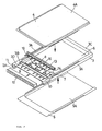
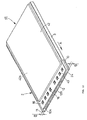
- FIGS. 1 through 12 A preferred embodiment will be now described with reference to FIGS. 1 through 12. First, a first embodiment of the present invention will be described below with reference to FIGS. 1 through 11.
- a PC card 1 of the instant embodiment is adapted for both the 16-bit and 32-bit slots.
- a casing 2 constitutes the contour of the PC card 1 and is formed in a thin plate shape.
- the casing 2 is composed of a frame 3 which is thin and has openings in the upper, lower sides, respectively, an upper panel 4 for lidding the upper opening of the frame 3 and having a rectangular bulgy portion 4A, and a lower panel 5 for lidding the lower opening of the frame 3 and having a bulgy portion 5A rectangular as well to define a space 6 for accommodating a board therein.
- a circuit board 7 is accommodated in the board-accommodating space 6 of the casing 2.
- a circuit is so configured and set on the board that an electronic component 8 mounted on the circuit board 7 is adaptable for processing of not only 32-bitbit bytes at a driving voltage of 3.3 V but also 16-bit bytes at a driving voltage of 5.0 V.
- Circuits adaptable for processing of 32-bit bytes at a driving voltage of 3.3 V and 16-bit bytes at a driving voltage of 5.0 V can be switched with a change-over switch (not shown) and the like, depending on the personal computer to which the PC card is attached.
- One side of the casing 2 is open to form a connector attaching port 2A.
- a card-side connector 12 is fixed into the connector attaching port 2A.
- An arrow A of FIG. 1 indicates the insertion direction of the PC card 1.
- the frame 3 is formed with a resin material in a rectangular shape, as shown in FIGS. 2 and 3.
- the frame 3 is composed of right- and left-hand side supports 3A separated from each other in the right- and left-hand side direction, and elongating between the front and the rear of the frame 3, a connecting beam 3B having a prism shape and connecting the supports 3A in the vicinity of the connector attaching port 2A, a connecting portion 3C connecting the supports 3A on the rear side, and a plate 3D positioned nearer to the connector attaching port 2A than the connecting beam 3B and on the upper face of the card-side connector 12 and elongating between the supports 3A.
- Plural (for example, eight holes) protuberance-accommodating holes 9 are formed in the plate 3D, as described below.
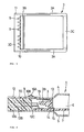
- the upper face of the card-side connector 12 is in contact with the lower side of the plate 3D (see FIG. 4).
- the plural protuberance accommodating holes 9 are formed in the plate 3D of the frame 3 in a rectangular shape.
- the spring protuberances 16 of the ground electrode 13 are projected through the protuberance-accommodating holes 9, respectively.
- a card-side key groove 10 is formed on the left-hand side of the PC card 1, viewed in the PC card insertion-direction.
- the card-side key groove 10 is provided on the side wall, present on the left-hand side thereof viewed in the insertion direction, of the frame 3 of the casing 2, in the vicinity of the connector attaching port 2A, and is formed by cutting the upper portion of the frame 3.
- the formed card-side key groove 10 has the groove width d1 which is equal to that of the card-side key groove of the16-bit PC card specified by the Standard.
- a guide groove 11 is formed on the right-hand side, viewed in the insertion direction, of the PC card 1.
- the guide groove 11 is positioned on the right-hand side of the frame 3 viewed in the insertion direction, in the vicinity of the connector attaching port 2A of the frame of the casing 11, and is formed by grooving the side wall of the frame.
- the formed guide groove 11 has a groove width d0 which is specified by the Standard.
- a long card-side connector 12 provided in the connector attaching port 2A of the casing 2 is composed of a rectangular member 12A formed with an insulation resin material in a long shape, totaled 68 pin holes 12B arranged in two rows of 34 pin holes and elongating from the front to the back of the rectangular member 12A, and terminal pins 12C of which the base ends are positioned in the inner parts of the pin holes 12B and the tips are projected from the back of the rectangular member 12A to be connected to the circuit board 7, respectively.
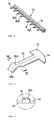
- a ground electrode 13 formed with an electro-conductive metal sheet is composed of a fixing frame 14 elongating along the connecting beam 3B of the frame 3 and so formed as to have a U-shaped cross section with which the connecting beam 3B is engaged, plural (for example, eight terminals) ground terminals 15 each elongating from the fixing frame 14 to ground on the circuit board 7 side (see FIG. 4), and spring protuberances 16 each elongating from the fixing frame 14 toward the upper face of the card-side connector 12.
- Each spring protuberance 16 is so formed that the tip side of its portion elongating from the fixing frame 14 is bent substantially into a chevron-shape, whereby the bent portion becomes a protuberant portion 16A and the tip 16B is a free end, elongating on the upper face of the card-side connector 12.
- the tip 16B of the spring protuberance 16 is placed and supported on the upper face of the card-side connector 12 (see FIG 4).
- each spring protuberance 16 is so formed as to have an arch-shape cross section in the projecting portion 16A. Therefore, flashes and the like, generated when the spring protuberance 16 is formed, can be directed inwardly of the spring protuberance 16. Therefore, the edges of the projecting portion 16A and its neighborhood, projected through the protuberance-accommodating hole 9, of the spring protuberance 16 is prevented from be caught in the protuberance-accommodating holes 9.
- the fixing frame 14 may be soldered directly on the ground on the circuit board 7 side.
- the PC card 1 of the instant embodiment has the above-described configuration.
- a 32-bit card slot conventionally used, will be described with reference to FIGS. 8 and 10.
- a 32-bit card slot 21 is composed mainly of a housing 22 having a card insertion hole 22A which has a size larger to some degree than the outside size of the PC card 1, and a slot-side connector 23 provided in the inner part of the card insertion hole 22A of the housing 22.
- the slot-side connector 23 is composed of a rectangular member 23A formed with a resin material in a long shape and having a connector insertion hole 23B into which the card-side connector 12 is inserted through the card insertion hole 22A, and totaled 68 connecting pins 23C positioned in the inner part of the connector insertion hole 23B formed in the rectangular member 23A, projecting therefrom, and arranged in two rows of 34 pins.
- the connecting pins 23C get into connection to the terminal pins 12C positioned in the inner parts of the pin holes 12B, respectively.
- a receiving ground electrode 24 formed in the upper part of the connector insertion hole 23B, as shown in FIG. 10, comprises plural (for example, eight pieces) contact pieces 24A which are directed downward so as to present spring properties.
- a slot-side key groove 25 is formed on the left-hand side viewed in the insertion direction of the PC card. As shown in FIG. 8, the slot-side key groove 25 is provided in the vicinity of the connector insertion hole 23B of the rectangular member 23A of the slot-side connector 23, positioned on the left-hand side viewed in the insertion direction, and is formed by grooving the side wall of the rectangular member 23A in the insertion direction.
- the formed slot-side key groove 25 has a wide groove width d2' which corresponds to that of the card-side key groove of the 32-bit PC card specified by the Standard.
- a guide protuberance 26 is formed on the right-hand side viewed in the PC card insertion direction, and as shown in FIG. 8, is provided in the vicinity of the connector insertion hole 23B of the rectangular member 23A of the slot-side connector 23 and, positioned on the right-hand side viewed in the insertion direction, and is formed by grooving the side wall of the rectangular member 23A in the insertion direction.
- the guide protuberance 26 has a thickness d0' which is thinner to some degree than the groove width d0 of the guide groove 11 of the PC card 1.
- a 16-bit card slot 31 is composed mainly of a housing 32 having a card insertion hole 32A which has a size larger to some degree than the outside size of the PC card 1, and a slot-side connector 33 provided in the inner part of the card insertion hole 32A of the housing 32.
- the slot-side connector 33 is composed of a rectangular member 33A formed with a resin material in a long shape, and having a connector insertion hole 33B into which the card-side connector 12 is inserted through the card insertion hole 32A, and totaled 68 connecting pins 33C positioned in the inner part of the connector insertion hole 33B, projecting therefrom, and arranged in two rows of 34 pins.
- the tips of the connecting pins 33C get into connection to the terminal pins 12C positioned in the inner parts of the pin holes 12B, respectively.
- a slot-side key groove 34 is formed on the left-hand side viewed in the insertion direction of the PC card. More particularly, the slot-side key groove 34 is provided in the vicinity of the connector insertion hole 33B of the rectangular member 33A of the slot-side connector 33, positioned on the left-hand side viewed in the insertion direction, and is formed by grooving the side wall of the rectangular member 33A along the insertion direction.
- the formed slot-side key groove 34 has a wide groove width d1' which corresponds to that of the card-side key groove of the 16-bit PC card specified by the Standard.
- a guide protuberance 35 is formed on the right-hand side viewed in the PC card insertion direction, and is provided in the vicinity of the connector insertion hole 33B of the rectangular member 33A of the slot-side connector 33, positioned on the right-hand side viewed in the insertion direction, and formed by grooving the side wall of the rectangular member 33A in the insertion direction.
- the guide protuberance 35 has a thickness d0' which is thinner to some degree than the groove width d0 of the guide groove 11 of the PC card 1.
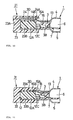
- Each spring protuberance 16 formed in the ground electrode 13 gets into contact with the contact piece 24A of the receiving ground electrode 24 on the 32-bit card slot side 21.
- the spring protuberance 16 given spring properties, is contacted with the contact piece 24A, to a high electric contact degree, further contributed by the spring force of the contact piece 24A.
- the PC card 1 can be attached into the 16-bit card slot 31 without damaging the card insertion hole 32A of the 16-bit card slot 31, the connector insertion hole 33B of the slot-side connector 33, and the like. Furthermore, after the PC card 1 is pulled out, each spring protuberance 16 is restored with its spring force. Therefore, the PC card can be inserted into the ordinary 32-bit card slot 21 as described above.
- the PC card 1 can be detachably inserted into both of the 32-bit and 16-bit card slots 21 and 31. That is, the PC card 1 is available for both 32-bit byte and 16-bit byte systems. Thus, the PC card 1 has a wider use range.
- each spring protuberance 16 is projected upwardly through the protuberance-accommodating hole 9 of the casing 2, and the tip 16B is extended on the card-side connector 12. Accordingly, when the PC card 1 is inserted into the 16-bit card-side slot 31, the tip 16B of the spring protuberance 16 is received and supported on the upper face of the card-side connector 12, so that the spring protuberance 16 is prevented from getting into contact with the terminal pin 12C of the card-side connector 12, enhancing the reliability of the PC card 1.
- each spring protuberance 16 When the PC card is pulled out of the 16-bit card-side slot 31, each spring protuberance 16 is restored with its spring force.
- the projection portion 16A of each spring protuberance 16 is so formed as to have a arc-shape cross section as shown in FIG. 7, which prevents the spring protuberance 16 from being caught in the protuberance-accommodating holes 9 when it is displaced.
- each protuberance-accommodating holes 9 surrounds the spring protuberance 16, the spring protuberance 16 is protected from being bent and damaged in event that an external force is applied to the spring protuberance 16 in the lateral direction. This is effective in increasing the service life of each spring protuberance 16.
- the ground electrode 13 is built in while the fixing frame 14 is engaged with the connecting beam 3B of the frame 3. Therefore, the work of soldering each ground terminal 15 of the ground electrode 13 onto the circuit board 7 can be simplified, improving the working efficiency of the assembly.
- the PC card 41 of the instant embodiment is characteristic in that the upper panel 42 constituting the casing 2 is provided with protuberance accommodating holes 43 in which each spring protuberance 16 of the ground electrode 13 is accommodated.
- PC card 41 of the instant embodiment operation and working effect similar to those of the PC card 1 of the above-described first embodiment can be obtained.
- the PC card 41 can be attached into both the 16-bit and 32-bit card slots.
- the spring protuberance 16 is so formed as to have an arc-shape cross section.
- the cross-section of the spring protuberance 16 may be bent by bending the sides of the spring protuberance inwardly.
- the PC card is described by way of 32-bit and 16-bit PC cards specified by the Standard.
- the present invention may be applied for the case that 64-bit and 128-bit PC cards specified by the Standard, are used with 16-bit card connectors, and so forth, and is not restricted on the specifications employed in the above embodiments.
- the frame of the casing is composed of the right-hand and left-hand supports and the connecting beam connecting the respective supports in the vicinity of the connector attaching port
- the ground electrode is composed of the fixing frame elongating along the connecting beam of the frame and engaged with the connecting beam
- the plural spring protuberances each elongating from the fixing frame toward one of the upper and lower flat faces of the connector. Therefore, for example, when the PC card is inserted into the lower-bit card slot having no parts for receiving the ground electrode, the spring protuberances are displaced toward the casing side, so that the PC card can be attached into the card slot.
- the PC card when the PC card is pulled out of the card slot, the spring protuberances are restored.
- the PC card can be attached into the higher-bit card slot having a part for receiving the ground electrode and also the lower-bit card slot having no parts for receiving the ground electrode.
- the PC card has wider use fields.
- the ground electrode is attached in the state that the fixing frame is engaged with the connecting beam of the frame, the joining work such as soldering and the like for connection of the ground electrode to ground on the circuit board side, conducted when the PC card is assembled, can be easily performed. The working efficiency of the assembly can be enhanced.
- the frame of the casing is provided with the plate which is located nearer to the connector attaching port than the connecting beam and on one of the flat faces of the connector, and is elongated between the supports, and the plate is provided with protuberance accommodating holes in which each spring protuberance of the ground electrode is to be accommodate.
- each spring protuberance of the ground electrode can be projected through the protuberance accommodating hole provided for the plate of the frame.
- the protuberance accommodating hole protects the spring protuberance from being damaged, increasing the service life of the spring protuberance.
- One of the upper and lower panels constituting the casing may be provided with protuberance accommodating holes in which each spring protuberance of the ground electrode is to be accommodated.
- each spring protuberance of the ground electrode can be projected through the protuberance accommodating hole of the panel.
- each spring protuberance of the ground electrode is formed as a plate spring of which the portion thereof elongating from said fixing frame is bent on its way.
- the spring protuberance of the ground electrode gets into contact with the insertion hole of the card slot.
- the PC card can be inserted into the card sloth in the state that the spring protuberance is distorted.
- each spring protuberance of the ground electrode which is projected from the casing is so formed as to have an arc-shape cross-section.
- the sides of the spring protuberance are prevented from being caught in the protuberance accommodating hole. This increases the service life of the spring protuberance.
Landscapes
- Coupling Device And Connection With Printed Circuit (AREA)
Claims (5)
- Eine PC-Karte (1), die folgende Merkmale aufweist:wobei der Rahmen (3) des Gehäuses (2) aus rechtsseitigen und linksseitigen Trägern (3A), die in der rechtsseitigen und der linksseitigen Richtung voneinander getrennt sind und sich von der Vorderseite zu der Rückseite des Rahmens (3) erstrecken, und aus einem Verbindungsbalken (3B), der die jeweiligen Träger (3A) in der Nähe des Verbinderbefestigungstors (2A) verbindet, gebildet ist,ein Gehäuse (2), das aus einem Rahmen (3) zum Aufnehmen einer Schaltungsplatine (7) und einer oberen und einer unteren Blende (4, 5) zum Abdecken des Rahmens (3) besteht und eine in einer Seite des Gehäuses (2) vorgesehene Öffnung als Verbinderbefestigungstor (2A) aufweist,einen Verbinder (12), der aus einem rechteckigen Bauglied (12A) gebildet ist, das mehrere Anschlußst:ifte (12C), die ausgelegt sind, um mit der Schaltungsplatine (7) verbunden zu werden, und mehrere Stiftlöcher (12B) aufweist, wobei Anschlußstifte auf der Personal-Computer-Seite ausgelegt sind, um in diese eingeführt zu werden, wobei der Verbinder (12) in dem Verbinderbefestigungstor (2A) des Gehäuses (2) angeordnet ist, um an dem Gehäuse (2) befestigt zu sein, undeine Masseelektrode (13) zum Verbinden der Masse der Schaltungsplatine (7) mit der Personal-Computer-Seite,
dadurch gekennzeichnet, daß
die Masseelektrode (13) aus einem Befestigungsrahmen (14), der sich entlang des Verbindungsbalkens (3B) des Rahmens (3) erstreckt und mit dem Verbindungsbalken (3B) in Eingriff steht, und mehreren Federvorsprüngen (16) gebildet ist, die sich jeweils von dem Befestigungsrahmen (14) hin zu entweder der oberen oder der unteren flachen Seite des Verbinders (12) erstrecken, wobei die mehreren Federvorsprünge (16) ausgelegt sind, um mit Abschnitten eines Kartenschlitzes (21; 31) in Kontakt zu treten und Federeigenschaften zu zeigen, wenn die PC-Karte in den Kartenschlitz (21; 31) auf der Personal-Computer-Seite eingeführt ist. - Eine PC-Karte (1) gemäß Anspruch 1, bei der der Rahmen (3) des Gehäuses (2) mit einer Platte (3D) versehen ist, die näher an dem Verbinderbefestigungstor (2A) als der Verbindungsbalken (3B) und auf einer der flachen Seiten des Verbinders (12) angeordnet ist und sich zwischen den Trägern (3A) erstreckt, und wobei die Platte (3D) mit Vorsprungsaufnahmelöchern (9) versehen ist, in denen jeder Federvorsprung (16) der Masseelektrode (13) aufgenommen werden soll.
- Eine PC-Karte (1) gemäß Anspruch 1, bei der entweder die obere oder die untere Blende (4, 5), die das Gehäuse (2) bilden, mit Vorsprungsaufnahmelöchern (9) versehen ist, in denen jeder Federvorsprung (16) der Masseelektrode (13) aufgenommen werden soll.
- Eine PC-Karte (1) gemäß einem der Ansprüche 1, 2 und 3, bei der jeder Federvorsprung (16) der Masseelektrode (13) als Blattfeder gebildet ist, bei der sich der Abschnitt, der sich von dem Befestigungsrahmen erstreckt, auf seinem Weg durchgebogen ist.
- Eine PC-Karte (1) gemäß einem der Ansprüche 1, 2, 3 und 4, bei der zumindest ein Teil jedes Federvorsprungs (16) der Masseelektrode (13), der von dem Gehäuse (2) vorsteht, gebildet ist, um einen bogenförmigen Querschnitt aufzuweisen.
Applications Claiming Priority (2)
| Application Number | Priority Date | Filing Date | Title |
|---|---|---|---|
| JP8299998 | 1998-03-13 | ||
| JP08299998A JP3159161B2 (ja) | 1998-03-13 | 1998-03-13 | Pcカード |
Publications (3)
| Publication Number | Publication Date |
|---|---|
| EP0942499A2 EP0942499A2 (de) | 1999-09-15 |
| EP0942499A3 EP0942499A3 (de) | 2001-12-05 |
| EP0942499B1 true EP0942499B1 (de) | 2003-05-28 |
Family
ID=13789933
Family Applications (1)
| Application Number | Title | Priority Date | Filing Date |
|---|---|---|---|
| EP99104919A Expired - Lifetime EP0942499B1 (de) | 1998-03-13 | 1999-03-11 | PC-Karte |
Country Status (6)
| Country | Link |
|---|---|
| US (1) | US6106309A (de) |
| EP (1) | EP0942499B1 (de) |
| JP (1) | JP3159161B2 (de) |
| DE (1) | DE69908218D1 (de) |
| SG (1) | SG74125A1 (de) |
| TW (1) | TW507166B (de) |
Families Citing this family (6)
| Publication number | Priority date | Publication date | Assignee | Title |
|---|---|---|---|---|
| JP3271588B2 (ja) * | 1998-07-10 | 2002-04-02 | 株式会社村田製作所 | Pcカード |
| JP4290272B2 (ja) * | 1999-04-20 | 2009-07-01 | 富士通コンポーネント株式会社 | カード形周辺装置 |
| DE10006848C1 (de) * | 2000-02-16 | 2001-06-21 | Itt Mfg Enterprises Inc | Steckkarte für elektronische Geräte |
| US6330163B1 (en) * | 2000-07-24 | 2001-12-11 | Itt Manufacturing Enterprises, Inc. | IC card with CardBus bridge |
| TWM249266U (en) * | 2003-07-30 | 2004-11-01 | Hon Hai Prec Ind Co Ltd | Electronic card connector |
| USD591752S1 (en) * | 2007-12-06 | 2009-05-05 | Sony Corporation | Memory card |
Family Cites Families (9)
| Publication number | Priority date | Publication date | Assignee | Title |
|---|---|---|---|---|
| US5330630A (en) * | 1991-01-02 | 1994-07-19 | Energy Conversion Devices, Inc. | Switch with improved threshold voltage |
| US5496185A (en) * | 1994-07-11 | 1996-03-05 | Samsung Electronics Co., Ltd. | Connecting device of data cable |
| US5478260A (en) * | 1994-07-29 | 1995-12-26 | The Whitaker Corporation | Grounding for electrical connectors |
| US5653596A (en) * | 1995-06-02 | 1997-08-05 | Molex Incorporated | Grounding system for PC cards |
| US5588850A (en) * | 1995-08-08 | 1996-12-31 | Tongrand Limited | Grounding means for memory card connector |
| JP3126102B2 (ja) * | 1995-08-11 | 2001-01-22 | ヒロセ電機株式会社 | Pcカード用ソケットコネクタ及びこれを有するpcカード |
| US5725394A (en) * | 1996-10-11 | 1998-03-10 | Molex Incorporated | Grounding system for IC cards |
| US5906496A (en) * | 1996-12-23 | 1999-05-25 | Thomas & Betts International, Inc. | Miniature card edge clip |
| US5833473A (en) * | 1997-03-12 | 1998-11-10 | Itt Manufacturing Enterprises, Inc. | Cardbus Bridge |
-
1998
- 1998-03-13 JP JP08299998A patent/JP3159161B2/ja not_active Expired - Fee Related
-
1999
- 1999-03-08 TW TW088103505A patent/TW507166B/zh not_active IP Right Cessation
- 1999-03-10 SG SG1999001084A patent/SG74125A1/en unknown
- 1999-03-11 EP EP99104919A patent/EP0942499B1/de not_active Expired - Lifetime
- 1999-03-11 DE DE69908218T patent/DE69908218D1/de not_active Expired - Lifetime
- 1999-03-12 US US09/267,836 patent/US6106309A/en not_active Expired - Fee Related
Also Published As
| Publication number | Publication date |
|---|---|
| JP3159161B2 (ja) | 2001-04-23 |
| US6106309A (en) | 2000-08-22 |
| JPH11265431A (ja) | 1999-09-28 |
| EP0942499A3 (de) | 2001-12-05 |
| TW507166B (en) | 2002-10-21 |
| SG74125A1 (en) | 2000-07-18 |
| DE69908218D1 (de) | 2003-07-03 |
| EP0942499A2 (de) | 1999-09-15 |
Similar Documents
| Publication | Publication Date | Title |
|---|---|---|
| JP2844530B2 (ja) | Icカード用のシールド | |
| US7134884B2 (en) | Electrical connector with high durability cycles | |
| US6074223A (en) | Compact flash card having a grounding tab | |
| US20030100218A1 (en) | Universal serial bus connector operable so as to indicate signal transmission status | |
| US6475005B2 (en) | Electrical card connector | |
| US6109969A (en) | Cable connector having improved EMI shields for securely grounding to a panel of a mating connector | |
| US6099353A (en) | IC card connector | |
| EP0942499B1 (de) | PC-Karte | |
| US6561816B1 (en) | Card connector with resilient grounding contact | |
| US6077127A (en) | Electrical connection device | |
| US6086420A (en) | I/O port connector | |
| US7044778B2 (en) | Connector having a shell which can readily be fixed to a connector housing | |
| EP0919933B1 (de) | Umschaltbare kompatible PC-Karte mit 16bit und 32bit modi | |
| US6604955B2 (en) | Electronic circuit protection device | |
| US6475031B1 (en) | Electrical connector having improved retention devices | |
| JP2003045574A (ja) | カードアダプタ | |
| US6213790B1 (en) | Information processing apparatus | |
| US6186801B1 (en) | PC card | |
| US6166892A (en) | Connector with built-in resettable power regulation | |
| JP3232225B2 (ja) | 情報カード、並びにそのためのバックコネクタ及びカードブランク | |
| US6475034B1 (en) | Electrical connector | |
| US7338325B2 (en) | Electrical adapter | |
| US6481633B1 (en) | IC incorporating card with a grounding structure | |
| JP3118215B2 (ja) | Pcカード | |
| JP3921963B2 (ja) | コネクタ |
Legal Events
| Date | Code | Title | Description |
|---|---|---|---|
| PUAI | Public reference made under article 153(3) epc to a published international application that has entered the european phase |
Free format text: ORIGINAL CODE: 0009012 |
|
| 17P | Request for examination filed |
Effective date: 19990311 |
|
| AK | Designated contracting states |
Kind code of ref document: A2 Designated state(s): AT BE CH CY DE DK ES FI FR GB GR IE IT LI LU MC NL PT SE Kind code of ref document: A2 Designated state(s): DE FR GB |
|
| AX | Request for extension of the european patent |
Free format text: AL;LT;LV;MK;RO;SI |
|
| PUAL | Search report despatched |
Free format text: ORIGINAL CODE: 0009013 |
|
| AK | Designated contracting states |
Kind code of ref document: A3 Designated state(s): AT BE CH CY DE DK ES FI FR GB GR IE IT LI LU MC NL PT SE |
|
| AX | Request for extension of the european patent |
Free format text: AL;LT;LV;MK;RO;SI |
|
| RIC1 | Information provided on ipc code assigned before grant |
Free format text: 7H 01R 23/70 A, 7H 01R 13/658 B |
|
| 17Q | First examination report despatched |
Effective date: 20020306 |
|
| AKX | Designation fees paid |
Free format text: DE FR GB |
|
| GRAH | Despatch of communication of intention to grant a patent |
Free format text: ORIGINAL CODE: EPIDOS IGRA |
|
| GRAH | Despatch of communication of intention to grant a patent |
Free format text: ORIGINAL CODE: EPIDOS IGRA |
|
| GRAA | (expected) grant |
Free format text: ORIGINAL CODE: 0009210 |
|
| RIC1 | Information provided on ipc code assigned before grant |
Ipc: 7H 01R 13/658 A |
|
| AK | Designated contracting states |
Designated state(s): DE FR GB |
|
| PG25 | Lapsed in a contracting state [announced via postgrant information from national office to epo] |
Ref country code: FR Free format text: LAPSE BECAUSE OF FAILURE TO SUBMIT A TRANSLATION OF THE DESCRIPTION OR TO PAY THE FEE WITHIN THE PRESCRIBED TIME-LIMIT Effective date: 20030528 |
|
| REG | Reference to a national code |
Ref country code: GB Ref legal event code: FG4D |
|
| REG | Reference to a national code |
Ref country code: IE Ref legal event code: FG4D |
|
| REF | Corresponds to: |
Ref document number: 69908218 Country of ref document: DE Date of ref document: 20030703 Kind code of ref document: P |
|
| PG25 | Lapsed in a contracting state [announced via postgrant information from national office to epo] |
Ref country code: DE Free format text: LAPSE BECAUSE OF FAILURE TO SUBMIT A TRANSLATION OF THE DESCRIPTION OR TO PAY THE FEE WITHIN THE PRESCRIBED TIME-LIMIT Effective date: 20030829 |
|
| PLBE | No opposition filed within time limit |
Free format text: ORIGINAL CODE: 0009261 |
|
| STAA | Information on the status of an ep patent application or granted ep patent |
Free format text: STATUS: NO OPPOSITION FILED WITHIN TIME LIMIT |
|
| 26N | No opposition filed |
Effective date: 20040302 |
|
| EN | Fr: translation not filed | ||
| REG | Reference to a national code |
Ref country code: IE Ref legal event code: MM4A |
|
| PGFP | Annual fee paid to national office [announced via postgrant information from national office to epo] |
Ref country code: GB Payment date: 20090311 Year of fee payment: 11 |
|
| GBPC | Gb: european patent ceased through non-payment of renewal fee |
Effective date: 20100311 |
|
| PG25 | Lapsed in a contracting state [announced via postgrant information from national office to epo] |
Ref country code: GB Free format text: LAPSE BECAUSE OF NON-PAYMENT OF DUE FEES Effective date: 20100311 |