EP0942500A2 - Appareil pour l'assemblage d'un connecteur électrique et procédé d'utilisation - Google Patents
Appareil pour l'assemblage d'un connecteur électrique et procédé d'utilisation Download PDFInfo
- Publication number
- EP0942500A2 EP0942500A2 EP99102847A EP99102847A EP0942500A2 EP 0942500 A2 EP0942500 A2 EP 0942500A2 EP 99102847 A EP99102847 A EP 99102847A EP 99102847 A EP99102847 A EP 99102847A EP 0942500 A2 EP0942500 A2 EP 0942500A2
- Authority
- EP
- European Patent Office
- Prior art keywords
- connectors
- connector
- shield
- plug
- receptacle
- Prior art date
- Legal status (The legal status is an assumption and is not a legal conclusion. Google has not performed a legal analysis and makes no representation as to the accuracy of the status listed.)
- Withdrawn
Links
Images









Classifications
-
- H—ELECTRICITY
- H01—ELECTRIC ELEMENTS
- H01R—ELECTRICALLY-CONDUCTIVE CONNECTIONS; STRUCTURAL ASSOCIATIONS OF A PLURALITY OF MUTUALLY-INSULATED ELECTRICAL CONNECTING ELEMENTS; COUPLING DEVICES; CURRENT COLLECTORS
- H01R43/00—Apparatus or processes specially adapted for manufacturing, assembling, maintaining, or repairing of line connectors or current collectors or for joining electric conductors
-
- H—ELECTRICITY
- H01—ELECTRIC ELEMENTS
- H01R—ELECTRICALLY-CONDUCTIVE CONNECTIONS; STRUCTURAL ASSOCIATIONS OF A PLURALITY OF MUTUALLY-INSULATED ELECTRICAL CONNECTING ELEMENTS; COUPLING DEVICES; CURRENT COLLECTORS
- H01R12/00—Structural associations of a plurality of mutually-insulated electrical connecting elements, specially adapted for printed circuits, e.g. printed circuit boards [PCB], flat or ribbon cables, or like generally planar structures, e.g. terminal strips, terminal blocks; Coupling devices specially adapted for printed circuits, flat or ribbon cables, or like generally planar structures; Terminals specially adapted for contact with, or insertion into, printed circuits, flat or ribbon cables, or like generally planar structures
- H01R12/70—Coupling devices
- H01R12/71—Coupling devices for rigid printing circuits or like structures
- H01R12/712—Coupling devices for rigid printing circuits or like structures co-operating with the surface of the printed circuit or with a coupling device exclusively provided on the surface of the printed circuit
- H01R12/716—Coupling device provided on the PCB
-
- H—ELECTRICITY
- H01—ELECTRIC ELEMENTS
- H01R—ELECTRICALLY-CONDUCTIVE CONNECTIONS; STRUCTURAL ASSOCIATIONS OF A PLURALITY OF MUTUALLY-INSULATED ELECTRICAL CONNECTING ELEMENTS; COUPLING DEVICES; CURRENT COLLECTORS
- H01R12/00—Structural associations of a plurality of mutually-insulated electrical connecting elements, specially adapted for printed circuits, e.g. printed circuit boards [PCB], flat or ribbon cables, or like generally planar structures, e.g. terminal strips, terminal blocks; Coupling devices specially adapted for printed circuits, flat or ribbon cables, or like generally planar structures; Terminals specially adapted for contact with, or insertion into, printed circuits, flat or ribbon cables, or like generally planar structures
- H01R12/70—Coupling devices
- H01R12/71—Coupling devices for rigid printing circuits or like structures
- H01R12/72—Coupling devices for rigid printing circuits or like structures coupling with the edge of the rigid printed circuits or like structures
- H01R12/722—Coupling devices for rigid printing circuits or like structures coupling with the edge of the rigid printed circuits or like structures coupling devices mounted on the edge of the printed circuits
- H01R12/725—Coupling devices for rigid printing circuits or like structures coupling with the edge of the rigid printed circuits or like structures coupling devices mounted on the edge of the printed circuits containing contact members presenting a contact carrying strip, e.g. edge-like strip
-
- H—ELECTRICITY
- H01—ELECTRIC ELEMENTS
- H01R—ELECTRICALLY-CONDUCTIVE CONNECTIONS; STRUCTURAL ASSOCIATIONS OF A PLURALITY OF MUTUALLY-INSULATED ELECTRICAL CONNECTING ELEMENTS; COUPLING DEVICES; CURRENT COLLECTORS
- H01R13/00—Details of coupling devices of the kinds covered by groups H01R12/70 or H01R24/00 - H01R33/00
- H01R13/648—Protective earth or shield arrangements on coupling devices, e.g. anti-static shielding
- H01R13/658—High frequency shielding arrangements, e.g. against EMI [Electro-Magnetic Interference] or EMP [Electro-Magnetic Pulse]
- H01R13/6581—Shield structure
- H01R13/6582—Shield structure with resilient means for engaging mating connector
-
- Y—GENERAL TAGGING OF NEW TECHNOLOGICAL DEVELOPMENTS; GENERAL TAGGING OF CROSS-SECTIONAL TECHNOLOGIES SPANNING OVER SEVERAL SECTIONS OF THE IPC; TECHNICAL SUBJECTS COVERED BY FORMER USPC CROSS-REFERENCE ART COLLECTIONS [XRACs] AND DIGESTS
- Y10—TECHNICAL SUBJECTS COVERED BY FORMER USPC
- Y10T—TECHNICAL SUBJECTS COVERED BY FORMER US CLASSIFICATION
- Y10T29/00—Metal working
- Y10T29/53—Means to assemble or disassemble
- Y10T29/5313—Means to assemble electrical device
- Y10T29/53265—Means to assemble electrical device with work-holder for assembly
Definitions
- metal latch engagement surfaces are formed directly from bent portions of the metal shield.
- Shielding performance is enhanced by providing opposed laterally extending flanges on the shields.
- the flanges have interfitting structures arranged along an outer edge or distal so that the flanges of adjacent connectors can be interfit, thereby enhancing shielding integrity and minimizing space requirements.
- Contacts for establishing electrical connection between the shield of the receptacle conductor and the mating plug connector have a flexural axis extending generally in alignment with the insertion axis of the mating connector. These contacts are canted inwardly from the shield and can be additionally compliant toward and away from the flexural axis. In a preferred embodiment, these contacts are formed integrally with the sheet metal shield.
- an apparatus for mounting an electrical connector on a PCI bracket comprising a base containing a plurality of apertures and at least one spring loaded eject pin, a contact support plate having a plurality of slots used to position contact tails on the connectors, a vertical clamp used to hold the connectors in place and a spring loaded plunger positioned in the base such that the PCI bracket is accurately positioned with respect to the connectors.
- Fig. 1 illustrates a receptacle connector 20.
- This receptacle comprises a molded plastic contact retaining body 22 having an integral rear wall 23.
- a plurality of conductive contact terminals 24 are retained on the retainer body 22.
- the body 22 is molded of a polymeric insulator material.
- a pair of upper guide members 23a (Figs. 1, 3 and 10) extend forwardly from the wall 23.
- the tails 24a of the terminals 24 extend rearwardly from the body 22 and, as shown, can comprise surface mount tails (Fig. 2).
- One or more pegs 26 may be integrally molded with insulator 22. The pegs 26 provide location and hold down functions when the connector is mounted on a printed circuit board.
- the shield 28 Surrounding the insulator 22 is a shield 28 formed of suitable metallic sheet material.
- the shield 28 includes a top wall 30, opposed side walls 32a and 32b and a rear wall 34.
- Side walls 32a and 32b include through hole tails 33 adapted to be inserted and soldered or press fit into plated through holes of the circuit board on which the connector is mounted.
- Back wall 34 carriers similar through hole tails 34c. Alternatively the shield tails can be configured for surface mounting.
- Rear wall 34 also includes tabs 34a and 34b that are wrapped over the rear portions of the side walls 32a and 32b.
- a latch 35 formed on body 22 holds rear wall 34 in position.
- the shield 28 also includes bottom wall portions 36a, 36b.
- the top wall 30, side walls 32a, 32b and bottom walls 36a, 36b define a generally rectangular opening or chamber 38 that is adapted to receive a mating plug connector (later described) adapted to be inserted into the receptacle 20 along the insertion axis A.
- the shield also includes a plurality of flanges that extend generally transverse to the direction of the insertion axis A. These include the top flange 40, a bottom flange formed of flange portions 56a, 56b and a pair of opposed side flanges 50a, 50b.
- a latch receiving slot 42 is formed in the top wall 30 and flange 40.
- a pair of latching shoulders 44a, 44b are formed along opposed sides of the slot 42.
- the shoulders 44a, 44b are preferably formed by bending to form in-turned tangs that have flat latching surfaces or shoulders that are generally perpendicular to the insertion axis A.
- This structure is adapted to cooperate with a latch arm mounted on a mating connector, as will be subsequently described. It is also designed to emulate sensory perceptions of such plugs latching into molded plastic housings.
- Each of the side flanges 50a, 50b is provided with interfitting sections along the distal edges of the flanges.
- these interfitting sections comprise a plurality of fingers 52a and 52b.
- the longitudinal axes of the fingers 52a are offset from the longitudinal axes of the fingers 52b so that, when similar receptacles 20a - 20d (Fig. 6) are placed in side by side relationship, the fingers are interleaved. This improves shielding for the assembled row of connectors and allows closer side by side spacing of the connectors.
- Fig. 1 As shown in Fig.
- the side flanges 50a, 50b are, prior to mounting, disposed at a slight angle ⁇ with respect to a transverse plane normal to the insertion axis A. These flanges are adapted to be flexed rearwardly to approximately a right angle position when the flanges are pushed against the back side of an equipment panel (not shown), against which the receptacles 20a - 20b are mounted.
- the shield 28 includes a plurality of contacts for assuring electrical connection between the receptacle 20 and a mating plug 60 (Fig. 8). These structures include the top contact members 46a and 46b, the side contact fingers 54a and 54b, and the bottom contact members 58a, 58b.
- the top contact members 46a, 46b are formed from the top wall 30 and are canted inwardly into the opening 38 along flexural axes D and E (Fig. 8). As shown in Fig. 7, the flexural axes D and E are preferably parallel to the insertion axis A, but could be disposed in angular relation thereto, up to about a 90° angle. As shown in Fig.
- the upper contact members 46a, 46b are disposed at an angle ⁇ with respect to a plane normal to the top wall 30a.
- the contacts 46a, 46b include compliant contact members 48a, 48b, preferably in the form of cantilevered arms that can be flexed toward the flexural axes D and E respectively.
- a plurality of forwardly extending contacts 54a, 54b are formed in the side walls 32a, 32b respectively. These contact fingers are positioned to engage side walls of the mating plug. Contact between the bottom walls 36a, 36b and the bottom surface of the plug is achieved through forwardly extending contact fingers 58a, 58b. Thus it can be seen that electrical contact is established between the top, bottom and side walls of the receptacle 20 and the plug 60.
- the shield 28 includes a front zone B, wherein the mating plug is surrounded on all four sides by the metal shield, and a rear zone C, wherein the insulator 22 is surrounded at the top and on the sides by the shield 28.
- the arrangement of the shield sections and surrounding relationship of the contacts 46a, 46b, 54a,54b, and 58a,58b ensures a low impedance connection between the shield 28 (and ultimately the printed circuit board) and the plug 60.
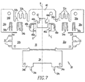
- Fig. 7 illustrates the flat blank from which the shield 28 is formed.
- the back wall 34 is formed by bending downwardly along the junction between wall 34 and top section 30.
- the tabs 34a, 34b are formed by bending the tabs forwardly at approximately a 90° angle to the back wall 34.
- Side walls 32a, 32b are formed by bending along the top wall edges generally parallel with insertion axis A.
- bottom walls 36a, 36b are formed by bending the shield along the junctions between the sections 36a, 36b and the side walls 32a, 32b.
- the flanges 40, 50a, 50b, and 56a, 56b, are similarly formed by bending from the blank shown in Fig. 1.
- the contact elements 46a, 46b, 54a, 54b and 58a, 58b are formed by stamping and bending from the blank shown in Figs. 1 and 2.
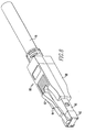
- a typical mating plug connector 60 is illustrated.
- This plug includes an insulative nose section 62 that serves as an insulator for contacts (not shown) that are carried on the bottom side of the nose and engage the receptacle contacts 24.
- the nose is preferably formed of an insulative polymeric material.
- a latch arm 63, having latching surfaces 64, is preferably integrally molded with the nose 62.
- the plug includes a metallic shield section 66 that surrounds the conductors within the plug from the nose 62 rearwardly toward the cable 70.
- the plug includes an overmold section 68 utilized primarily for gripping the plug.
- the side contacts 54a, 54b engage the side walls of the shield 66 to establish an electrical connection therewith.
- the front wall of the nose section 62 is positioned against the wall 23 of insulator 22.
- the nose section is held in vertical location by the body 22 and the guide sections 23a.
- the top contact 46a, 46b engage the top wall of shield 66 via the cantilever arms 48a and 48b.
- the forwardly extending bottom contact members 58a, 58b engage the bottom surface of the shield 66.
- the top contact members 46a and 46b touch the top surface of the shield 66 of the plug.
- the upper contacts 46a, 46b are capable of being deflected by rotation about the flexural axes D and E respectively and by compliance of the cantilevered arms 48a, 48b. This structure allows the generation of substantial normal forces by the upper contacts 46a and 46b within the relatively limited axial length of the zone B of shield 28.
- the plug 60 and receptacle 20 are held in mated condition by the engagement of the latch surfaces 64 with the bent latch tangs 44a, 44b. Release of the plug is permitted by pressing the latch arm 63 downwardly toward the shield 66 to release the surfaces 64 from the tangs 44a, 44b.
- the described features above result in an interconnection system that has improved shielding and overall lower impedance. As a result, higher signal frequencies can be passed through this interconnection system within acceptable levels of signal degradation.
- the improved performance is believed to result, at least in part, by minimization of the length of ground paths from the plug to the printed circuit board as a result of the location and/or orientation of the various grounding contacts formed in the shield.
- the latching structure described provides essentially the same tactile feel and aural sensation as achieved with latch structures formed in molded plastic housings. Thus the user has the same sensory perceptions that occur when the plug latch assumes the latched position or is unlatched with the disclosed structure as with previous molded receptacle housings.
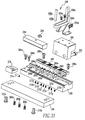
- This apparatus includes a base plate 266 which includes PCI eject springs 268a, 268b and 268c.
- the base plate 266 is also connected to the rest of the assembly by means of fasteners 270a and 270b.
- superimposed over the base plate there are connector peg springs 272a - 272h.
- a connector spacer 282 Superimposed on the base plate there is a connector spacer 282 and fasteners 284 and 284b, ejector pegs 286a - 286b and fasteners 288 and 288b. Also superimposed on the alignment plate is a clamp bracket 290 which is attached to the apparatus assembly by means of bolts as at 292.
- the apparatus assembly also includes a hold-down block 294 and a fastening nut 296 as well as a clamp assembly shown generally at 298 which is held to the clamp bracket 290 by means of fasteners 300a, 300b, 300c and 300d.
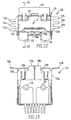
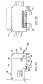
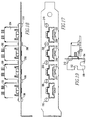
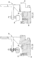
- receptacle as is shown in Figs. 12 - 16 may be mounted on a PCI bracket.
- the contact support plate which has a series of slots is used to accurately position or re-position any of the contact tails as the connectors are being loaded into the fixture.
- a vertical clamp is used to hold the connectors in place.
- a spring loaded plunger and a series of internal springs in the base are used to accurately position the PCI bracket with respect to the connectors.
- the PCI bracket is permanently attached to the connectors using a support bracket and machine screws. The clamp is then removed which allows the eject pins to lift out the fixture with the completed PCI bracket.
Landscapes
- Engineering & Computer Science (AREA)
- Manufacturing & Machinery (AREA)
- Manufacturing Of Electrical Connectors (AREA)
- Details Of Connecting Devices For Male And Female Coupling (AREA)
- Coupling Device And Connection With Printed Circuit (AREA)
Applications Claiming Priority (4)
| Application Number | Priority Date | Filing Date | Title |
|---|---|---|---|
| US77497 | 1987-07-24 | ||
| US7749798P | 1998-03-11 | 1998-03-11 | |
| US09/211,291 US6231403B1 (en) | 1997-03-07 | 1998-12-14 | Apparatus for assembling an electrical connector and method of use |
| US211291 | 1998-12-14 |
Publications (2)
| Publication Number | Publication Date |
|---|---|
| EP0942500A2 true EP0942500A2 (fr) | 1999-09-15 |
| EP0942500A3 EP0942500A3 (fr) | 2000-01-19 |
Family
ID=26759336
Family Applications (1)
| Application Number | Title | Priority Date | Filing Date |
|---|---|---|---|
| EP99102847A Withdrawn EP0942500A3 (fr) | 1998-03-11 | 1999-03-01 | Appareil pour l'assemblage d'un connecteur électrique et procédé d'utilisation |
Country Status (3)
| Country | Link |
|---|---|
| US (1) | US6231403B1 (fr) |
| EP (1) | EP0942500A3 (fr) |
| JP (1) | JPH11317275A (fr) |
Families Citing this family (3)
| Publication number | Priority date | Publication date | Assignee | Title |
|---|---|---|---|---|
| WO2002076169A1 (fr) * | 2001-03-16 | 2002-09-26 | Laird Technologies, Inc. | Coquille de protection pour emetteur-recepteur par fibres optiques |
| CN201360060Y (zh) | 2008-12-22 | 2009-12-09 | 上海莫仕连接器有限公司 | 电连接器 |
| CN117680970A (zh) * | 2023-12-28 | 2024-03-12 | 沈阳兴华航空电器有限责任公司 | 一种插孔组件内簧装配设备 |
Family Cites Families (26)
| Publication number | Priority date | Publication date | Assignee | Title |
|---|---|---|---|---|
| US3601890A (en) | 1969-11-04 | 1971-08-31 | Federal Tool Eng Co | Method of and apparatus for fabricating contacts and assembling them in groups with connector blocks |
| US3729809A (en) * | 1971-11-22 | 1973-05-01 | Rohr Industries Inc | Nut plate riveting device |
| US3952392A (en) * | 1974-01-11 | 1976-04-27 | Bunker Ramo Corporation | Field termination tool having connector reference plane apparatus and hinged insertion arms |
| US4383361A (en) | 1981-09-17 | 1983-05-17 | Amp Incorporated | Connector insertion tool |
| US4520555A (en) * | 1982-09-27 | 1985-06-04 | Magnetic Information Technology, Inc. | Apparatus and method for aligning and assembly of a gimbal, magnetic slider head, and flexure arm |
| US4488581A (en) | 1983-05-19 | 1984-12-18 | Amp Incorporated | Terminal alignment tool |
| US4837926A (en) | 1988-05-31 | 1989-06-13 | Amp Incorporated | Work holder for electrical connectors |
| JPH0716312Y2 (ja) | 1989-02-28 | 1995-04-12 | ホシデン株式会社 | コネクタ |
| US4906201A (en) | 1989-05-25 | 1990-03-06 | Tektronix, Inc. | Electrical connector mounting apparatus with EMI shielding |
| US4970781A (en) * | 1989-08-10 | 1990-11-20 | Olin Corporation | Process plate for plastic pin grid array manufacturing |
| US4967470A (en) | 1990-04-20 | 1990-11-06 | Amp Incorporated | Alignment apparatus for positioning a connector housing during wire insertion |
| US5085590A (en) | 1990-10-30 | 1992-02-04 | Amp Incorporated | Shielded stackable connector assembly |
| US5161997A (en) | 1991-10-11 | 1992-11-10 | Amp Incorporated | Hardwareless panel retention for shielded connector |
| US5623754A (en) * | 1992-10-01 | 1997-04-29 | Chick Machine Tool, Inc. | Apparatus for facilitating the detachment of an element from an object |
| US5600881A (en) | 1993-05-13 | 1997-02-11 | Itt Corporation | Connector seating press |
| JP2836725B2 (ja) | 1993-11-29 | 1998-12-14 | 矢崎総業株式会社 | 端子挿入方法及び端子挿入装置 |
| DE4414036A1 (de) * | 1994-04-22 | 1995-10-26 | Behr Gmbh & Co | Lufteintritt für eine Heizungs- oder Klimaanlage eines Kraftfahrzeugs |
| US5475916A (en) * | 1994-11-21 | 1995-12-19 | The Whitaker Corporation | Machine for staking a two part connector housing together |
| JPH08236258A (ja) * | 1995-02-27 | 1996-09-13 | Sumitomo Wiring Syst Ltd | コネクタ保持装置 |
| US5815917A (en) | 1995-05-17 | 1998-10-06 | Berg Technology, Inc. | Method and apparatus for mounting an electrical connector on a printed wiring board |
| FR2734420B1 (fr) | 1995-05-18 | 1998-08-07 | Amp France | Support de connecteurs pour machines de fabrication de faisceaux |
| DE69627455T2 (de) | 1995-11-24 | 2004-03-25 | Victor Company of Japan, Ltd., Yokohama | Verbindungsanordnung |
| US5685739A (en) | 1996-02-14 | 1997-11-11 | The Whitaker Corporation | Shielded electrical connector |
| US5702271A (en) | 1996-08-30 | 1997-12-30 | The Whitaker Corporation | Ultra low profile board-mounted modular jack |
| US5896649A (en) * | 1997-03-26 | 1999-04-27 | The Whitaker Corporation | Seating tool for installing electrical connectors to printed circuit boards |
| US6078504A (en) * | 1997-10-08 | 2000-06-20 | Cisco Systems, Inc. | Universal adapter bracket for communications devices |
-
1998
- 1998-12-14 US US09/211,291 patent/US6231403B1/en not_active Expired - Fee Related
-
1999
- 1999-03-01 EP EP99102847A patent/EP0942500A3/fr not_active Withdrawn
- 1999-03-11 JP JP11064892A patent/JPH11317275A/ja active Pending
Also Published As
| Publication number | Publication date |
|---|---|
| EP0942500A3 (fr) | 2000-01-19 |
| JPH11317275A (ja) | 1999-11-16 |
| US6231403B1 (en) | 2001-05-15 |
Similar Documents
| Publication | Publication Date | Title |
|---|---|---|
| US6733339B2 (en) | Shielded connector with integral latching and ground structure | |
| EP0863581B1 (fr) | Blindage pour connecteur électrique avec verrouillage et contacts de masse | |
| US6454603B2 (en) | Shielded connector with integral latching and ground structure | |
| US4894026A (en) | Miniature circular DIN connector | |
| US4679879A (en) | Plug and receptacle connector assembly | |
| EP0460975B1 (fr) | Connecteurs avec structure de mise à la terre | |
| US5685739A (en) | Shielded electrical connector | |
| EP0658953B1 (fr) | Ensemble de douilles modulaires multiple | |
| EP0907989B1 (fr) | Connecteur electrique blinde | |
| EP1610421B1 (fr) | Connecteur avec connection à la terre fiable | |
| EP0928049A2 (fr) | Connecteurs empilés pour un réseau local | |
| WO1998009352A1 (fr) | Jack modulaire de tres faible hauteur monte sur une plaquette | |
| EP0624928A1 (fr) | Assemblage de connecteur électrique blindé | |
| WO1998013904A1 (fr) | Ensemble connecteur hybride mis a la masse et comportant des plots audio empiles | |
| US6296518B1 (en) | Stacked electrical connector assembly | |
| US4737888A (en) | Receptacle assembly and mounting bracket for circuit board connections | |
| EP0370833B1 (fr) | Connecteur din circulaire miniature | |
| US6231403B1 (en) | Apparatus for assembling an electrical connector and method of use | |
| KR960002137B1 (ko) | 소형의 원형 din 접속기 | |
| EP0995239A1 (fr) | Appareil permettant de former une connexion a travers une carte |
Legal Events
| Date | Code | Title | Description |
|---|---|---|---|
| PUAI | Public reference made under article 153(3) epc to a published international application that has entered the european phase |
Free format text: ORIGINAL CODE: 0009012 |
|
| AK | Designated contracting states |
Kind code of ref document: A2 Designated state(s): BE CH DE DK ES FI FR GB IE IT LI SE |
|
| AX | Request for extension of the european patent |
Free format text: AL;LT;LV;MK;RO;SI |
|
| PUAL | Search report despatched |
Free format text: ORIGINAL CODE: 0009013 |
|
| AK | Designated contracting states |
Kind code of ref document: A3 Designated state(s): AT BE CH CY DE DK ES FI FR GB GR IE IT LI LU MC NL PT SE |
|
| AX | Request for extension of the european patent |
Free format text: AL;LT;LV;MK;RO;SI |
|
| RIC1 | Information provided on ipc code assigned before grant |
Free format text: 7H 01R 43/00 A, 7H 01R 23/68 B, 7H 05K 7/14 B |
|
| 17P | Request for examination filed |
Effective date: 20000707 |
|
| AKX | Designation fees paid |
Free format text: BE CH DE DK ES FI FR GB IE IT LI SE |
|
| 17Q | First examination report despatched |
Effective date: 20001030 |
|
| STAA | Information on the status of an ep patent application or granted ep patent |
Free format text: STATUS: THE APPLICATION IS DEEMED TO BE WITHDRAWN |
|
| 18D | Application deemed to be withdrawn |
Effective date: 20020411 |