EP0943440A2 - Tintenstrahlaufzeichnungskopf und Herstellungsverfahren - Google Patents
Tintenstrahlaufzeichnungskopf und Herstellungsverfahren Download PDFInfo
- Publication number
- EP0943440A2 EP0943440A2 EP99105653A EP99105653A EP0943440A2 EP 0943440 A2 EP0943440 A2 EP 0943440A2 EP 99105653 A EP99105653 A EP 99105653A EP 99105653 A EP99105653 A EP 99105653A EP 0943440 A2 EP0943440 A2 EP 0943440A2
- Authority
- EP
- European Patent Office
- Prior art keywords
- ink
- channel
- electrode
- jet recording
- recording head
- Prior art date
- Legal status (The legal status is an assumption and is not a legal conclusion. Google has not performed a legal analysis and makes no representation as to the accuracy of the status listed.)
- Withdrawn
Links
Images





Classifications
-
- B—PERFORMING OPERATIONS; TRANSPORTING
- B41—PRINTING; LINING MACHINES; TYPEWRITERS; STAMPS
- B41J—TYPEWRITERS; SELECTIVE PRINTING MECHANISMS, i.e. MECHANISMS PRINTING OTHERWISE THAN FROM A FORME; CORRECTION OF TYPOGRAPHICAL ERRORS
- B41J2/00—Typewriters or selective printing mechanisms characterised by the printing or marking process for which they are designed
- B41J2/005—Typewriters or selective printing mechanisms characterised by the printing or marking process for which they are designed characterised by bringing liquid or particles selectively into contact with a printing material
- B41J2/01—Ink jet
- B41J2/135—Nozzles
- B41J2/16—Production of nozzles
- B41J2/1621—Manufacturing processes
- B41J2/1623—Manufacturing processes bonding and adhesion
-
- B—PERFORMING OPERATIONS; TRANSPORTING
- B41—PRINTING; LINING MACHINES; TYPEWRITERS; STAMPS
- B41J—TYPEWRITERS; SELECTIVE PRINTING MECHANISMS, i.e. MECHANISMS PRINTING OTHERWISE THAN FROM A FORME; CORRECTION OF TYPOGRAPHICAL ERRORS
- B41J2/00—Typewriters or selective printing mechanisms characterised by the printing or marking process for which they are designed
- B41J2/005—Typewriters or selective printing mechanisms characterised by the printing or marking process for which they are designed characterised by bringing liquid or particles selectively into contact with a printing material
- B41J2/01—Ink jet
- B41J2/135—Nozzles
- B41J2/14—Structure thereof only for on-demand ink jet heads
- B41J2/14201—Structure of print heads with piezoelectric elements
- B41J2/14209—Structure of print heads with piezoelectric elements of finger type, chamber walls consisting integrally of piezoelectric material
-
- B—PERFORMING OPERATIONS; TRANSPORTING
- B41—PRINTING; LINING MACHINES; TYPEWRITERS; STAMPS
- B41J—TYPEWRITERS; SELECTIVE PRINTING MECHANISMS, i.e. MECHANISMS PRINTING OTHERWISE THAN FROM A FORME; CORRECTION OF TYPOGRAPHICAL ERRORS
- B41J2/00—Typewriters or selective printing mechanisms characterised by the printing or marking process for which they are designed
- B41J2/005—Typewriters or selective printing mechanisms characterised by the printing or marking process for which they are designed characterised by bringing liquid or particles selectively into contact with a printing material
- B41J2/01—Ink jet
- B41J2/135—Nozzles
- B41J2/16—Production of nozzles
- B41J2/1607—Production of print heads with piezoelectric elements
- B41J2/1609—Production of print heads with piezoelectric elements of finger type, chamber walls consisting integrally of piezoelectric material
-
- B—PERFORMING OPERATIONS; TRANSPORTING
- B41—PRINTING; LINING MACHINES; TYPEWRITERS; STAMPS
- B41J—TYPEWRITERS; SELECTIVE PRINTING MECHANISMS, i.e. MECHANISMS PRINTING OTHERWISE THAN FROM A FORME; CORRECTION OF TYPOGRAPHICAL ERRORS
- B41J2/00—Typewriters or selective printing mechanisms characterised by the printing or marking process for which they are designed
- B41J2/005—Typewriters or selective printing mechanisms characterised by the printing or marking process for which they are designed characterised by bringing liquid or particles selectively into contact with a printing material
- B41J2/01—Ink jet
- B41J2/135—Nozzles
- B41J2/16—Production of nozzles
- B41J2/1621—Manufacturing processes
- B41J2/1626—Manufacturing processes etching
- B41J2/1628—Manufacturing processes etching dry etching
-
- B—PERFORMING OPERATIONS; TRANSPORTING
- B41—PRINTING; LINING MACHINES; TYPEWRITERS; STAMPS
- B41J—TYPEWRITERS; SELECTIVE PRINTING MECHANISMS, i.e. MECHANISMS PRINTING OTHERWISE THAN FROM A FORME; CORRECTION OF TYPOGRAPHICAL ERRORS
- B41J2/00—Typewriters or selective printing mechanisms characterised by the printing or marking process for which they are designed
- B41J2/005—Typewriters or selective printing mechanisms characterised by the printing or marking process for which they are designed characterised by bringing liquid or particles selectively into contact with a printing material
- B41J2/01—Ink jet
- B41J2/135—Nozzles
- B41J2/16—Production of nozzles
- B41J2/1621—Manufacturing processes
- B41J2/1631—Manufacturing processes photolithography
-
- B—PERFORMING OPERATIONS; TRANSPORTING
- B41—PRINTING; LINING MACHINES; TYPEWRITERS; STAMPS
- B41J—TYPEWRITERS; SELECTIVE PRINTING MECHANISMS, i.e. MECHANISMS PRINTING OTHERWISE THAN FROM A FORME; CORRECTION OF TYPOGRAPHICAL ERRORS
- B41J2/00—Typewriters or selective printing mechanisms characterised by the printing or marking process for which they are designed
- B41J2/005—Typewriters or selective printing mechanisms characterised by the printing or marking process for which they are designed characterised by bringing liquid or particles selectively into contact with a printing material
- B41J2/01—Ink jet
- B41J2/135—Nozzles
- B41J2/16—Production of nozzles
- B41J2/1621—Manufacturing processes
- B41J2/1632—Manufacturing processes machining
-
- B—PERFORMING OPERATIONS; TRANSPORTING
- B41—PRINTING; LINING MACHINES; TYPEWRITERS; STAMPS
- B41J—TYPEWRITERS; SELECTIVE PRINTING MECHANISMS, i.e. MECHANISMS PRINTING OTHERWISE THAN FROM A FORME; CORRECTION OF TYPOGRAPHICAL ERRORS
- B41J2/00—Typewriters or selective printing mechanisms characterised by the printing or marking process for which they are designed
- B41J2/005—Typewriters or selective printing mechanisms characterised by the printing or marking process for which they are designed characterised by bringing liquid or particles selectively into contact with a printing material
- B41J2/01—Ink jet
- B41J2/135—Nozzles
- B41J2/16—Production of nozzles
- B41J2/1621—Manufacturing processes
- B41J2/164—Manufacturing processes thin film formation
- B41J2/1642—Manufacturing processes thin film formation thin film formation by CVD [chemical vapor deposition]
-
- B—PERFORMING OPERATIONS; TRANSPORTING
- B41—PRINTING; LINING MACHINES; TYPEWRITERS; STAMPS
- B41J—TYPEWRITERS; SELECTIVE PRINTING MECHANISMS, i.e. MECHANISMS PRINTING OTHERWISE THAN FROM A FORME; CORRECTION OF TYPOGRAPHICAL ERRORS
- B41J2/00—Typewriters or selective printing mechanisms characterised by the printing or marking process for which they are designed
- B41J2/005—Typewriters or selective printing mechanisms characterised by the printing or marking process for which they are designed characterised by bringing liquid or particles selectively into contact with a printing material
- B41J2/01—Ink jet
- B41J2/135—Nozzles
- B41J2/16—Production of nozzles
- B41J2/1621—Manufacturing processes
- B41J2/164—Manufacturing processes thin film formation
- B41J2/1646—Manufacturing processes thin film formation thin film formation by sputtering
-
- B—PERFORMING OPERATIONS; TRANSPORTING
- B41—PRINTING; LINING MACHINES; TYPEWRITERS; STAMPS
- B41J—TYPEWRITERS; SELECTIVE PRINTING MECHANISMS, i.e. MECHANISMS PRINTING OTHERWISE THAN FROM A FORME; CORRECTION OF TYPOGRAPHICAL ERRORS
- B41J2/00—Typewriters or selective printing mechanisms characterised by the printing or marking process for which they are designed
- B41J2/005—Typewriters or selective printing mechanisms characterised by the printing or marking process for which they are designed characterised by bringing liquid or particles selectively into contact with a printing material
- B41J2/01—Ink jet
- B41J2/135—Nozzles
- B41J2/14—Structure thereof only for on-demand ink jet heads
- B41J2002/14379—Edge shooter
-
- B—PERFORMING OPERATIONS; TRANSPORTING
- B41—PRINTING; LINING MACHINES; TYPEWRITERS; STAMPS
- B41J—TYPEWRITERS; SELECTIVE PRINTING MECHANISMS, i.e. MECHANISMS PRINTING OTHERWISE THAN FROM A FORME; CORRECTION OF TYPOGRAPHICAL ERRORS
- B41J2/00—Typewriters or selective printing mechanisms characterised by the printing or marking process for which they are designed
- B41J2/005—Typewriters or selective printing mechanisms characterised by the printing or marking process for which they are designed characterised by bringing liquid or particles selectively into contact with a printing material
- B41J2/01—Ink jet
- B41J2/135—Nozzles
- B41J2/14—Structure thereof only for on-demand ink jet heads
- B41J2002/14491—Electrical connection
-
- Y—GENERAL TAGGING OF NEW TECHNOLOGICAL DEVELOPMENTS; GENERAL TAGGING OF CROSS-SECTIONAL TECHNOLOGIES SPANNING OVER SEVERAL SECTIONS OF THE IPC; TECHNICAL SUBJECTS COVERED BY FORMER USPC CROSS-REFERENCE ART COLLECTIONS [XRACs] AND DIGESTS
- Y10—TECHNICAL SUBJECTS COVERED BY FORMER USPC
- Y10T—TECHNICAL SUBJECTS COVERED BY FORMER US CLASSIFICATION
- Y10T29/00—Metal working
- Y10T29/49—Method of mechanical manufacture
- Y10T29/49002—Electrical device making
- Y10T29/49117—Conductor or circuit manufacturing
- Y10T29/49124—On flat or curved insulated base, e.g., printed circuit, etc.
- Y10T29/49128—Assembling formed circuit to base
-
- Y—GENERAL TAGGING OF NEW TECHNOLOGICAL DEVELOPMENTS; GENERAL TAGGING OF CROSS-SECTIONAL TECHNOLOGIES SPANNING OVER SEVERAL SECTIONS OF THE IPC; TECHNICAL SUBJECTS COVERED BY FORMER USPC CROSS-REFERENCE ART COLLECTIONS [XRACs] AND DIGESTS
- Y10—TECHNICAL SUBJECTS COVERED BY FORMER USPC
- Y10T—TECHNICAL SUBJECTS COVERED BY FORMER US CLASSIFICATION
- Y10T29/00—Metal working
- Y10T29/49—Method of mechanical manufacture
- Y10T29/49002—Electrical device making
- Y10T29/49117—Conductor or circuit manufacturing
- Y10T29/49124—On flat or curved insulated base, e.g., printed circuit, etc.
- Y10T29/49155—Manufacturing circuit on or in base
-
- Y—GENERAL TAGGING OF NEW TECHNOLOGICAL DEVELOPMENTS; GENERAL TAGGING OF CROSS-SECTIONAL TECHNOLOGIES SPANNING OVER SEVERAL SECTIONS OF THE IPC; TECHNICAL SUBJECTS COVERED BY FORMER USPC CROSS-REFERENCE ART COLLECTIONS [XRACs] AND DIGESTS
- Y10—TECHNICAL SUBJECTS COVERED BY FORMER USPC
- Y10T—TECHNICAL SUBJECTS COVERED BY FORMER US CLASSIFICATION
- Y10T29/00—Metal working
- Y10T29/49—Method of mechanical manufacture
- Y10T29/49401—Fluid pattern dispersing device making, e.g., ink jet
Definitions
- the present invention relates to an ink jet recording head and a manufacturing method thereof. More to particularly, this invention relates to an ink jet recording head and a manufacturing method thereof, in which it is capable of being arranged multi-nozzle and high density nozzle , being in use for a printer, facsimile, or copying machine.
- this kind of the ink jet recording device is capable of being divided into largely two classes in terms of point of ink discharge drive source.
- thermal ink jet or bubble jet for instance, being disclosed in the Japanese Patent Publication No. SHO 61-59913.
- This method is a method in which pressure chambers are formed in answer to respective thermal elements on a thermal head to which a plurality of thermal elements are arranged, and a nozzle and an ink supply path open to the pressure chamber, at the time of printing, causing the thermal element to be energized to heat an ink to be generated bubble, so that it causes the ink to be discharged from the nozzle by virtue of the pressure of the bubble.
- a thermal head which is a discharge source is capable of being manufactured by photo-lithography technology so that there can be formed printing head with high density and multi-nozzle, thus enabling small-sized and high-speed ink jet recording device to be obtained.
- the other one is a method so called as a piezoelectric method, for instance, being disclosed in the Japanese Patent Publication No. SHO 53-12138.
- the piezoelectric method consists of a pressure chamber together opening into both of a nozzle and an ink supply path, and a piezoelectric element generating volume change to the pressure chamber. At the time of printing, there is applied voltage to the piezoelectric element in order to generate the volume change to the pressure chamber to be discharged ink from the nozzle.
- the degree of freedom of ink selection is high, and to be long life, however, it is difficult to arrange many piezoelectric elements in high density, it is difficult to obtain small-sized and high speed ink jet recording device.
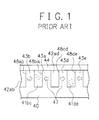
- Fig. 1 in terms of the Japanese Patent Application Laid-Open No. HEI 6-143564.
- ink channels 41bc, 41 de, ⁇ , and dummy channels 42ab, 42cd, ⁇ whose upper side covered with a top plate 44, and whose sides thereof surrounded by partition walls 43b, 43c, 43d, 43e, ⁇ , on a substrate 40 made of the piezoelectric element formed into one piece of plate made of piezoelectric material.
- the ink is filled into only 41bc, 41de, ⁇
- the partitions 43b, 43c, 43d, 43e, ⁇ polarize the partitions 43b, 43c, 43d, 43e, ⁇ , as an arrow (polarization direction 47) using electrodes 48bc, 48cd, 48de, ⁇ formed in the channel.
- the direction of the polarization which is directed to opposite direction with each other at the adjacent partitions therebetween.
- an ink jet recording head and a manufacturing method thereof in which there is prevented occurrence of ink electrolysis caused by individual configuration of ink jet recording head using piezoelectric body and mechanism.
- an ink jet recording head in which an ink channel and a dummy channel are formed alternately in such a way that a side wall of a piezoelectric body intervenes between the ink channel and the dummy channel, thus there is discharged an ink drop while changing volume within the ink channel by applying an electric field to a channel using an electrode formed within respective channels, wherein an electrode formed on respective the ink channels is taken as a common electrode, while an electrode formed on respective the dummy channels is taken as an individual electrode, causing no ink to be contacted with a passivation film formed on the individual electrode.
- an ink jet recording head which comprises a plate consisting of a piezoelectric body, a groove formed on the plate, a channel in which there exists an electrode on the inside of the groove, and whose both sides are partitioned by a side wall of the piezoelectric body, and whose upper side is covered by a top plate, a nozzle opening into the channel; and a control system including a voltage apply means for applying an electric field to the electrode, in which the side wall intervenes adjacent ink channels therebetween so as to be held in common by the adjacent ink channels, there is taken alternate channel filled with an ink as an ink channel and another channel as dummy channel, thus causing ink drop to be discharged from the nozzle while deforming the wall of both sides constituting the ink channel, wherein there is taken an electrode formed on the ink channel as a common electrode, while it causes no ink to be contacted with a passivation film on an individual electrode formed on the dummy channel.
- a manufacturing method of the ink jet recording head which comprises the steps of forming a groove for functioning as an ink channel and a dummy channel on a piezoelectric body, forming an electrode layer on the inside of the groove, forming a passivation film on said electrode layer, uniting a nozzle plate and a top plate after forming the passivation film, and forming a slit at the top plate, wherein when there is formed the slit at the top plate, there is formed individual electrode by separating the electrode layer while implementing groove formation to the bottom surface of the dummy channel.
- Fig. 2 is a perspective view , partly in section showing ink jet recording head according to an embodiment of the present invention.
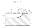
- Fig. 3 is a sectional view along line A - A' of Fig. 2.
- ink channels 1ab, 1cd, 1ef, and dummy channels 2bc, 2de, ⁇ are surrounded by side walls 3a, 3b, 3c, 3d, 3e, ⁇ consisting of a piezoelectric body 11 in terms of both sides and lower side, and surrounded by a top plate 8 and a nozzle plate in terms of respective upper side and front side.
- an ink pool 12 opening into the ink channels 1ab, 1cd, ⁇ through an ink supply opening 9 at the rear side of the ink channels 1ab, 1cd, ⁇
- the individual electrode of 4cd is provided so as to connect the side of the side wall 3c of the dummy channel 2bc with the side of the side wall 3d of the dummy channel 2de.
- interlayer isolation film 13 at the region where the individual electrodes 4ab, 4cd, ⁇ and the common electrode 5 cross, and a passivation film 14 at the portion where is exposed in the channel of the common electrode 5, respectively.
- the ink (not illustrated) is filled with the ink channels 1ab, 1cd, ⁇ , the nozzles 6ab, 6cd, ⁇ , and the ink pool 12.
- the side walls 3a, 3b, 3c, 3d, 3e, ⁇ , consisting of the piezoelectric body 11 are given polarization processing in the width direction (in the arrow P direction) thereof.
- the top plate 8 has flexibility and there are provided slits 10 separated on the dummy channels 2bc, 2de, ⁇ .
- the length of the ink channels 1ab, 1cd, ⁇ is longer than the length of the dummy channels 2bc, 2de, ⁇ . The reason why there is intended that it causes the ink to be filled with only ink channel because the slits 10 are provided with the top plate 8 on the dummy channels 2bc, 2de, ⁇ . There is supplied the ink filled within the ink pool to the ink channel from the ink supply opening 9.
- Fig. 3 is a sectional view along line A - A' of Fig. 2.
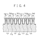
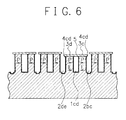
- Figs. 4 to 7 are explanation views of operation corresponding to the sectional view along line B - B' of the ink jet recording head shown in Fig. 2. Referring to Figs. 4 to 7, there will be described the case where it causes certain specified ink channel 1cd to be driven out of a plurality of ink channels 1ab, 1cd, ⁇ , thus discharging ink drop from the nozzle 6cd (not illustrated) opening into the ink channel 1cd.
- the drive of the ink channel means that it causes the side walls 3c, and 3d to be driven, the side walls 3c, and 3d comprising the piezoelectric body 11 of the both sides which constitute the ink channel.
- the side walls 3c, and 3d shrink in the electric field direction, while expand in the vertical direction to the electric field direction, because the polarization direction (the arrow P direction) is reverse direction of the electric field direction (the arrow E direction.
- the ink is supplied to the ink channel 1cd from the ink pool only corresponding quantity of volume increase, because volume of the ink channel increases so that pressure decreases.
- the ink drop is discharged from the nozzle 6cd, because volume of the ink channel decreases so that pressure increases.
- volume of the ink channel decreases so that pressure increases.
- It enables the ink drop to be discharged while changing the state of Fig. 4 into the state of Fig. 6 directly by pressure increase of the ink channel. It is capable of controlling position of meniscus by entering the state of Fig. 5 in between.
- the ink supply to the ink channel is implemented with the two states of Figs. 5 and 7. There is stabilized the speed of the ink drop and frequency characteristics of drop diameter so that it is capable of being implemented suitable discharge of the ink drop.
- the ink channel is always of the grounded, and the ink does not contact completely with the passivation film 14 on the individual electrodes 4ab, 4cd, ⁇ . Consequently, the electric field does not affect the ink at the time of drive, thus there does not occur the electrolysis of the ink completely, which occurs generally caused by the defect of the passivation film 14, or caused by the electronic withstand voltage failure without defect.
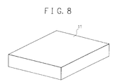
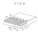
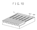
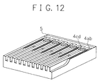
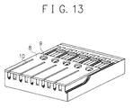
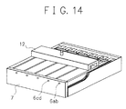
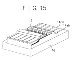
- Figs 8 to 15 are perspective views showing the ink jet recording head in every manufacturing process. There is roughly classified into 6 processes of a channel formation, an electrode formation, a protective layer formation, a slit formation, and a gluing process.
- Fig. 8 in the channel formation process, firstly, as shown in Fig. 8, there is implemented channel formation such that there are alternately arranged grooves functioning by way of the ink channels 1ab, 1cd, ⁇ , and grooves functioning by way of the dummy channels 2bc, 2de, ⁇ , toward the piezoelectric body 11 consisting of 3component system soft ceramics that perovskite system complex oxide is added to PZT, by machining of the dicing saw shown in Fig. 9.
- length of the ink channels 1ab, 1cd, ⁇ are larger than the dummy channels 2bc, 2de, ⁇ , and end section of the ink pool side of the groove has a curvature.
- a first process is that film of aluminum is formed by sputtering by way of electrode layer so as to cover whole groove, thus forming the common electrode 5 and parts of individual electrodes 4ab, 4cd, ⁇ , using photolithography technology as shown in Fig. 10.
- parts of individual electrodes 4ab. 4cd, ⁇ are region with the exception of parts of the common electrode 5 crossing.
- the electrode layer which is capable of being formed of aluminum alloy such as aluminum-copper, aluminum-silicon, aluminum-silicon-copper by sputtering or vapor deposition.
- a second process is to form the interlayer isolation film 13 on the common electrode 5 at the region shown in Fig. 11. At this time, the groove section undergoes masking, thus there is formed the isolation film only at the plane section. The required pattern is obtained using photolithography technology thereafter.
- interlayer isolation film 13 which is capable of being formed such that silicon dioxide, silicon nitride, BPSG film, macromolecule material undergo CVD, sputtering and so forth.
- the patterning of the interlayer isolation film is to use dry etching.
- a third process is to form remaining section of the individual electrodes 4ab, 4cd, ⁇ , as shown in Fig. 12.
- the remaining section means that the section to which the common electrode 5 crosses, which is not formed in Fig. 10.
- the groove section undergoes the masking, there is formed the film of electrode layer at the plane section.
- the required pattern is obtained using photolithography technology thereafter.
- the passivation film 14 by way of the protective layer formation to form to whole surface (including groove) with the exception of pad section. It is desirable to form the passivation film 14 such that silicon dioxide or BPSB film with suitable wetting property undergoes the CVD with suitable step coverage because the passivation film 14 touches the ink directly.
- the gluing process is to glue the top plate 8 of polyimide in which the ink supply opening 9 is formed beforehand such that the top plate 8 covers the dummy channels 2bc, 2de, ⁇ , completely, and opening into the ink channels 1ab, 1cd, ⁇ , and the ink supply opening 9. It permits the top plate 8 to be isolated on the dummy channels 2bc, 2de, ⁇ , and the slit 10 to be formed deeply more than bottom section by means of the dicing saw. This state will be shown in Fig. 13.
- the slit is to form at the bottom section of the dummy channels 2bc, 2de, ⁇ , in order to isolate the individual electrodes completely. At this time point, there is formed the individual electrodes functioning completely.
- material with high rigidity such as ceramics, glass, silicon, and so forth instead of polyimide in which there is applied thermoplastic adhesive or thermosetting adhesive on one side by way of the top plate.
- nozzle plate 7 As shown in Fig. 14, there is glued the nozzle plate 7 at end surface of the ink channels 1ab, 1cd, ⁇ , such that there opens the plurality of nozzles 6ab, 6cd, ⁇ , formed through excimer laser processing on the nozzle plate 7 of polyimide into the ink channels 1ab, 1cd, ⁇ , thereafter.
- ink pool 12 of PS polysulfone
- silicon system adhesive sheet so as to cover the ink supplying opening 9 thereafter.
- thin plate such as nickel, and stainless steel, instead of polyimide in which there is applied thermoplastic adhesive or thermosetting adhesive on one side by way of the nozzle plate 7.
- a print substrate 16 to the bottom surface of the piezoelectric body 11.
- lead terminal sections 14ab, 14cd, ⁇ for connecting electrically to the pad section, thus being connected electrically to a drive circuit (not illustrated).
- the pad section is connected to the lead terminal sections 14ab, 14cd, ⁇ , by wire bonding 15.
- gold by way of material of the bonding wire 15.
- shape of end section of nozzle side of the ink channel has a curvature.
- the curvature contributes to stabilization of discharge of the ink drop in that air penetrating within the ink channel becomes difficult to be trapped, thus being improved air discharge property and flow of the ink becomes smooth.
- the ink jet recording head of the present invention causes the electrode to function as the common electrode, formed in the ink channel, and having a constitution causes no ink to be contacted with the passivation film on the individual electrode formed on the dummy channel, therefore, at the time of the driving, the electric field does not affect to the ink, there does not occur the electrolysis of the ink completely, which generally occurs caused by defect of the passivation film 14, or caused by electric withstanding voltage failure without the defect. This is to contribute to long life of the head, and to high print quality because there does not occur change of physical property of the ink during driving perfectly.
- the manufacturing method of the ink jet recording head of the present invention enables electrode separation within the dummy channel to be implemented at the same time of the slit formation, thus it is capable of being manufactured the ink jet recording head in stable state, in low cost, and accurately.
- the air discharging property is excellent, thus contributing to stabilization of ink drop discharging.
- the ink jet recording head of the present invention there is taken the electrode formed on the ink channel as the common electrode, and causing no ink to be contacted with the passivation film on the individual electrode formed at the dummy channel, for that reason, it is capable of being prevented occurrence of the electrolysis of the ink, thus there is the effect that it becomes possible to implement long life print, and high quality print.
- the manufacturing method of the ink jet recording head of the present invention since there are implemented both of the individual electrodes formation and the slit formation in the same manufacturing process, there is the effect that it is capable of manufactured in low cost, and in the stable state.
Landscapes
- Engineering & Computer Science (AREA)
- Manufacturing & Machinery (AREA)
- Particle Formation And Scattering Control In Inkjet Printers (AREA)
Applications Claiming Priority (2)
| Application Number | Priority Date | Filing Date | Title |
|---|---|---|---|
| JP10090670A JP2873287B1 (ja) | 1998-03-20 | 1998-03-20 | インクジェット記録ヘッドおよびその製造方法 |
| JP9067098 | 1998-03-20 |
Publications (2)
| Publication Number | Publication Date |
|---|---|
| EP0943440A2 true EP0943440A2 (de) | 1999-09-22 |
| EP0943440A3 EP0943440A3 (de) | 2000-05-03 |
Family
ID=14004983
Family Applications (1)
| Application Number | Title | Priority Date | Filing Date |
|---|---|---|---|
| EP99105653A Withdrawn EP0943440A3 (de) | 1998-03-20 | 1999-03-19 | Tintenstrahlaufzeichnungskopf und Herstellungsverfahren |
Country Status (3)
| Country | Link |
|---|---|
| US (2) | US6361151B1 (de) |
| EP (1) | EP0943440A3 (de) |
| JP (1) | JP2873287B1 (de) |
Cited By (5)
| Publication number | Priority date | Publication date | Assignee | Title |
|---|---|---|---|---|
| WO2002084751A1 (en) | 2001-04-06 | 2002-10-24 | Ngk Insulators,Ltd. | Cell drive type actuator and manufacturing method |
| EP1518682A1 (de) * | 2003-09-24 | 2005-03-30 | Brother Kogyo Kabushiki Kaisha | Tintenstrahldruckkopf und dazugehöriges Überprüfungsverfahren |
| GB2510029A (en) * | 2012-11-19 | 2014-07-23 | Sii Printek Inc | Liquid jet head having common and active electrodes |
| EP3199349A1 (de) * | 2016-01-29 | 2017-08-02 | Toshiba TEC Kabushiki Kaisha | Tintenstrahlkopf und tintenstrahldrucker |
| CN110816057A (zh) * | 2018-08-09 | 2020-02-21 | 东芝泰格有限公司 | 喷墨头、喷墨装置以及喷墨头的制造方法 |
Families Citing this family (28)
| Publication number | Priority date | Publication date | Assignee | Title |
|---|---|---|---|---|
| JP2002029049A (ja) * | 2000-07-14 | 2002-01-29 | Brother Ind Ltd | インクジェットヘッドおよびその製造方法 |
| US20020085067A1 (en) * | 2000-12-29 | 2002-07-04 | Robert Palifka | Ink jet printing module |
| JP2002205393A (ja) * | 2001-01-11 | 2002-07-23 | Seiko Instruments Inc | インクジェットヘッド及びインクジェット式記録装置並びにヘッドのゴミ除去方法 |
| US6933663B2 (en) * | 2001-04-06 | 2005-08-23 | Ngk Insulators, Ltd. | Cell driving type actuator and method for manufacturing the same |
| JP4662519B2 (ja) * | 2001-06-01 | 2011-03-30 | エスアイアイ・プリンテック株式会社 | ヘッドチップ、ヘッドチップユニット、インクジェット式記録装置、及びヘッドチップの製造方法。 |
| JP4694727B2 (ja) * | 2001-07-18 | 2011-06-08 | エスアイアイ・プリンテック株式会社 | ヘッドチップユニット及びインクジェット式記録装置 |
| JP4269721B2 (ja) * | 2002-03-07 | 2009-05-27 | コニカミノルタホールディングス株式会社 | インクジェットヘッドの製造方法 |
| JP4473532B2 (ja) * | 2002-10-10 | 2010-06-02 | 日本碍子株式会社 | 圧電/電歪デバイス及び製造方法 |
| JP4842520B2 (ja) | 2003-05-30 | 2011-12-21 | 日本碍子株式会社 | セル駆動型圧電/電歪アクチュエータ及びその製造方法 |
| JP4878111B2 (ja) * | 2003-10-30 | 2012-02-15 | 日本碍子株式会社 | セル駆動型圧電/電歪アクチュエータ及びその製造方法 |
| US7097280B2 (en) * | 2004-02-12 | 2006-08-29 | Lexmark International, Inc. | Printheads having improved heater chip construction |
| US20050275701A1 (en) * | 2004-06-14 | 2005-12-15 | Brother Kogyo Kabushiki Kaisha | Water base ink for ink-jet recording |
| JP4193836B2 (ja) * | 2005-10-24 | 2008-12-10 | ブラザー工業株式会社 | インク噴射装置の製造方法 |
| JP5056309B2 (ja) * | 2006-11-16 | 2012-10-24 | コニカミノルタIj株式会社 | インクジェットヘッド |
| JP5291347B2 (ja) * | 2008-01-11 | 2013-09-18 | エスアイアイ・プリンテック株式会社 | インクジェットヘッドチップ、インクジェットヘッドチップの駆動方法、インクジェットヘッド、及びインクジェット記録装置 |
| WO2010036235A1 (en) * | 2008-09-23 | 2010-04-01 | Hewlett-Packard Development Company, L.P. | Removing piezoelectric material using electromagnetic radiation |
| JP5804875B2 (ja) * | 2011-09-29 | 2015-11-04 | キヤノン株式会社 | 液体吐出ヘッド |
| JP5891096B2 (ja) | 2012-04-12 | 2016-03-22 | エスアイアイ・プリンテック株式会社 | 液体噴射ヘッドの製造方法、液体噴射ヘッド及び液体噴射装置 |
| JP5740422B2 (ja) * | 2013-03-06 | 2015-06-24 | 株式会社東芝 | インクジェットヘッドおよびインクジェット記録装置 |
| JP6314057B2 (ja) * | 2014-08-19 | 2018-04-18 | エスアイアイ・プリンテック株式会社 | 液体噴射ヘッド及び液体噴射装置 |
| CN106799892B (zh) * | 2015-11-26 | 2018-06-12 | 东芝泰格有限公司 | 喷墨头及喷墨记录装置 |
| US10427413B2 (en) * | 2016-05-20 | 2019-10-01 | Canon Kabushiki Kaisha | Liquid ejection head |
| JP6921565B2 (ja) * | 2016-05-20 | 2021-08-18 | キヤノン株式会社 | 液体吐出ヘッド |
| JP6868411B2 (ja) * | 2017-02-03 | 2021-05-12 | エスアイアイ・プリンテック株式会社 | 液体噴射ヘッドチップ、液体噴射ヘッド、液体噴射装置および液体噴射ヘッドチップの製造方法 |
| JP6909606B2 (ja) * | 2017-03-22 | 2021-07-28 | エスアイアイ・プリンテック株式会社 | 液体噴射ヘッドチップの製造方法 |
| JP6909605B2 (ja) * | 2017-03-22 | 2021-07-28 | エスアイアイ・プリンテック株式会社 | 液体噴射ヘッドチップ、液体噴射ヘッド、液体噴射装置および液体噴射ヘッドチップの製造方法 |
| JP7005156B2 (ja) * | 2017-03-22 | 2022-01-21 | エスアイアイ・プリンテック株式会社 | 液体噴射ヘッドチップの製造方法 |
| JP7506521B2 (ja) * | 2020-05-19 | 2024-06-26 | 東芝テック株式会社 | 液体吐出ヘッド及び液体吐出装置 |
Family Cites Families (13)
| Publication number | Priority date | Publication date | Assignee | Title |
|---|---|---|---|---|
| JPS5912828B2 (ja) | 1976-07-19 | 1984-03-26 | 株式会社大林組 | 鉄筋コンクリ−ト構造骨組の柱・梁接合部 |
| JPS6159913A (ja) | 1984-08-30 | 1986-03-27 | Shin Kobe Electric Mach Co Ltd | Ad変換回路 |
| JPH04348949A (ja) | 1991-05-28 | 1992-12-03 | Brother Ind Ltd | 液滴噴射装置 |
| US5432540A (en) * | 1992-02-25 | 1995-07-11 | Citizen Watch Co., Ltd. | Ink jet head |
| JPH06143564A (ja) | 1992-10-30 | 1994-05-24 | Citizen Watch Co Ltd | インクジェットヘッド |
| JPH06171096A (ja) | 1992-12-03 | 1994-06-21 | Brother Ind Ltd | インク噴射装置の製造方法及びインク噴射装置 |
| US5650810A (en) * | 1992-12-03 | 1997-07-22 | Brother Kogyo Kabushiki Kaisha | Ink jet print head having a manifold wall portion and method of producing the same by injection molding |
| US5646661A (en) | 1993-11-11 | 1997-07-08 | Brother Kogyo Kabushiki Kaisha | Ink ejecting device having alternating ejecting channels and non-ejecting channels |
| JP3183010B2 (ja) | 1993-12-24 | 2001-07-03 | ブラザー工業株式会社 | インク噴射装置 |
| US5535494A (en) * | 1994-09-23 | 1996-07-16 | Compaq Computer Corporation | Method of fabricating a piezoelectric ink jet printhead assembly |
| JP3166530B2 (ja) * | 1995-01-30 | 2001-05-14 | ブラザー工業株式会社 | インク噴射装置 |
| JPH0939233A (ja) | 1995-07-27 | 1997-02-10 | Brother Ind Ltd | インクジェットヘッド |
| US6106106A (en) * | 1997-01-14 | 2000-08-22 | Nec Corporation | Ink jet recording head having a piezoelectric substrate |
-
1998
- 1998-03-20 JP JP10090670A patent/JP2873287B1/ja not_active Expired - Fee Related
-
1999
- 1999-03-19 US US09/272,307 patent/US6361151B1/en not_active Expired - Fee Related
- 1999-03-19 EP EP99105653A patent/EP0943440A3/de not_active Withdrawn
-
2001
- 2001-04-26 US US09/843,626 patent/US6658737B2/en not_active Expired - Fee Related
Cited By (10)
| Publication number | Priority date | Publication date | Assignee | Title |
|---|---|---|---|---|
| WO2002084751A1 (en) | 2001-04-06 | 2002-10-24 | Ngk Insulators,Ltd. | Cell drive type actuator and manufacturing method |
| EP1376710A4 (de) * | 2001-04-06 | 2007-05-30 | Ngk Insulators Ltd | Stellelement des zellenansteuertyps und herstellungsverfahren |
| EP1518682A1 (de) * | 2003-09-24 | 2005-03-30 | Brother Kogyo Kabushiki Kaisha | Tintenstrahldruckkopf und dazugehöriges Überprüfungsverfahren |
| US7168792B2 (en) | 2003-09-24 | 2007-01-30 | Brother Kogyo Kabushiki Kaisha | Ink jet printer head and method of inspecting same |
| GB2510029A (en) * | 2012-11-19 | 2014-07-23 | Sii Printek Inc | Liquid jet head having common and active electrodes |
| US8967774B2 (en) | 2012-11-19 | 2015-03-03 | Sii Printek Inc. | Liquid jet head, liquid jet apparatus, and method of manufacturing liquid jet head |
| EP3199349A1 (de) * | 2016-01-29 | 2017-08-02 | Toshiba TEC Kabushiki Kaisha | Tintenstrahlkopf und tintenstrahldrucker |
| CN107020814A (zh) * | 2016-01-29 | 2017-08-08 | 东芝泰格有限公司 | 喷墨头及喷墨打印机 |
| CN107020814B (zh) * | 2016-01-29 | 2018-06-12 | 东芝泰格有限公司 | 喷墨头及喷墨打印机 |
| CN110816057A (zh) * | 2018-08-09 | 2020-02-21 | 东芝泰格有限公司 | 喷墨头、喷墨装置以及喷墨头的制造方法 |
Also Published As
| Publication number | Publication date |
|---|---|
| EP0943440A3 (de) | 2000-05-03 |
| JP2873287B1 (ja) | 1999-03-24 |
| US6361151B1 (en) | 2002-03-26 |
| US6658737B2 (en) | 2003-12-09 |
| JPH11268271A (ja) | 1999-10-05 |
| US20010030673A1 (en) | 2001-10-18 |
Similar Documents
| Publication | Publication Date | Title |
|---|---|---|
| EP0943440A2 (de) | Tintenstrahlaufzeichnungskopf und Herstellungsverfahren | |
| EP0857572B1 (de) | Tintenstrahlaufzeichnungskopf mit einem piezoelektrischen Substrat | |
| US6109738A (en) | Ink jet print head and a method of manufacturing the same | |
| EP0875380B1 (de) | Tintenstrahlaufzeichnungskopf | |
| JP3931976B2 (ja) | アクチュエータ装置及びインクジェット式記録ヘッド並びにインクジェット式記録装置 | |
| US7591542B2 (en) | Piezoelectric actuator, method for producing the same and ink-jet head | |
| JP3221470B2 (ja) | インクジェットヘッド、及びその製造方法 | |
| EP1083048A1 (de) | Tintenstrahldruckkopf und verfahren zur dessen herstellung | |
| EP1100684B1 (de) | Tintenstrahldruckkopf und verfahren zu seiner herstellung | |
| JP3738804B2 (ja) | インクジェット式記録ヘッド及びインクジェット式記録装置 | |
| JP3217006B2 (ja) | インクジェット記録ヘッドおよびその製造方法 | |
| JP4186084B2 (ja) | インクジェット式記録ヘッド及びインクジェット式記録装置 | |
| JP3468279B2 (ja) | 圧電振動子ユニットの製造方法 | |
| JP3551748B2 (ja) | インクジェット式記録ヘッド | |
| JPH11179903A (ja) | アクチュエータ及びインクジェット式記録ヘッド | |
| JPH0858090A (ja) | インク噴射装置及びその製造方法 | |
| JPH09327911A (ja) | インクジェットプリンタヘッド | |
| JP2005153243A (ja) | 液体噴射ヘッド及びその製造方法並びに液体噴射装置 | |
| JP3541638B2 (ja) | インクジェット式記録ヘッド | |
| JPH11291493A (ja) | インクジェット式記録ヘッド | |
| JP3552017B2 (ja) | インクジェット式記録ヘッド | |
| JP3690098B2 (ja) | インクジェット式記録ヘッド | |
| JP4120954B2 (ja) | 静電型アクチュエータ及びインクジェットヘッド、画像形成装置 | |
| JPH11300961A (ja) | インクジェット式記録ヘッド及びその製造方法 | |
| JP3633811B2 (ja) | インクジェット式記録ヘッド及びインクジェット式記録装置 |
Legal Events
| Date | Code | Title | Description |
|---|---|---|---|
| PUAI | Public reference made under article 153(3) epc to a published international application that has entered the european phase |
Free format text: ORIGINAL CODE: 0009012 |
|
| AK | Designated contracting states |
Kind code of ref document: A2 Designated state(s): DE FR GB IT |
|
| AX | Request for extension of the european patent |
Free format text: AL;LT;LV;MK;RO;SI |
|
| PUAL | Search report despatched |
Free format text: ORIGINAL CODE: 0009013 |
|
| AK | Designated contracting states |
Kind code of ref document: A3 Designated state(s): AT BE CH CY DE DK ES FI FR GB GR IE IT LI LU MC NL PT SE |
|
| AX | Request for extension of the european patent |
Free format text: AL;LT;LV;MK;RO;SI |
|
| 17P | Request for examination filed |
Effective date: 20000331 |
|
| AKX | Designation fees paid |
Free format text: DE FR GB IT |
|
| RAP1 | Party data changed (applicant data changed or rights of an application transferred) |
Owner name: FUJI XEROX CO., LTD. |
|
| STAA | Information on the status of an ep patent application or granted ep patent |
Free format text: STATUS: THE APPLICATION IS DEEMED TO BE WITHDRAWN |
|
| 18D | Application deemed to be withdrawn |
Effective date: 20031001 |