EP0943978A1 - Processeur a faible consommation d'energie - Google Patents
Processeur a faible consommation d'energie Download PDFInfo
- Publication number
- EP0943978A1 EP0943978A1 EP97913423A EP97913423A EP0943978A1 EP 0943978 A1 EP0943978 A1 EP 0943978A1 EP 97913423 A EP97913423 A EP 97913423A EP 97913423 A EP97913423 A EP 97913423A EP 0943978 A1 EP0943978 A1 EP 0943978A1
- Authority
- EP
- European Patent Office
- Prior art keywords
- circuit
- substrate
- mode
- voltages
- main circuit
- Prior art date
- Legal status (The legal status is an assumption and is not a legal conclusion. Google has not performed a legal analysis and makes no representation as to the accuracy of the status listed.)
- Withdrawn
Links
Images







Classifications
-
- G—PHYSICS
- G06—COMPUTING OR CALCULATING; COUNTING
- G06F—ELECTRIC DIGITAL DATA PROCESSING
- G06F1/00—Details not covered by groups G06F3/00 - G06F13/00 and G06F21/00
- G06F1/26—Power supply means, e.g. regulation thereof
- G06F1/32—Means for saving power
- G06F1/3203—Power management, i.e. event-based initiation of a power-saving mode
- G06F1/3234—Power saving characterised by the action undertaken
- G06F1/3296—Power saving characterised by the action undertaken by lowering the supply or operating voltage
-
- G—PHYSICS
- G06—COMPUTING OR CALCULATING; COUNTING
- G06F—ELECTRIC DIGITAL DATA PROCESSING
- G06F1/00—Details not covered by groups G06F3/00 - G06F13/00 and G06F21/00
- G06F1/04—Generating or distributing clock signals or signals derived directly therefrom
-
- G—PHYSICS
- G06—COMPUTING OR CALCULATING; COUNTING
- G06F—ELECTRIC DIGITAL DATA PROCESSING
- G06F1/00—Details not covered by groups G06F3/00 - G06F13/00 and G06F21/00
- G06F1/26—Power supply means, e.g. regulation thereof
- G06F1/32—Means for saving power
- G06F1/3203—Power management, i.e. event-based initiation of a power-saving mode
-
- Y—GENERAL TAGGING OF NEW TECHNOLOGICAL DEVELOPMENTS; GENERAL TAGGING OF CROSS-SECTIONAL TECHNOLOGIES SPANNING OVER SEVERAL SECTIONS OF THE IPC; TECHNICAL SUBJECTS COVERED BY FORMER USPC CROSS-REFERENCE ART COLLECTIONS [XRACs] AND DIGESTS
- Y02—TECHNOLOGIES OR APPLICATIONS FOR MITIGATION OR ADAPTATION AGAINST CLIMATE CHANGE
- Y02D—CLIMATE CHANGE MITIGATION TECHNOLOGIES IN INFORMATION AND COMMUNICATION TECHNOLOGIES [ICT], I.E. INFORMATION AND COMMUNICATION TECHNOLOGIES AIMING AT THE REDUCTION OF THEIR OWN ENERGY USE
- Y02D10/00—Energy efficient computing, e.g. low power processors, power management or thermal management
-
- Y—GENERAL TAGGING OF NEW TECHNOLOGICAL DEVELOPMENTS; GENERAL TAGGING OF CROSS-SECTIONAL TECHNOLOGIES SPANNING OVER SEVERAL SECTIONS OF THE IPC; TECHNICAL SUBJECTS COVERED BY FORMER USPC CROSS-REFERENCE ART COLLECTIONS [XRACs] AND DIGESTS
- Y02—TECHNOLOGIES OR APPLICATIONS FOR MITIGATION OR ADAPTATION AGAINST CLIMATE CHANGE
- Y02D—CLIMATE CHANGE MITIGATION TECHNOLOGIES IN INFORMATION AND COMMUNICATION TECHNOLOGIES [ICT], I.E. INFORMATION AND COMMUNICATION TECHNOLOGIES AIMING AT THE REDUCTION OF THEIR OWN ENERGY USE
- Y02D30/00—Reducing energy consumption in communication networks
- Y02D30/50—Reducing energy consumption in communication networks in wire-line communication networks, e.g. low power modes or reduced link rate
Definitions
- the present invention relates to a semiconductor integrated circuit device such as a processor, and more particularly to a microprocessor which is capable of realizing the high speed operation as well as the low power consumption by controlling substrate biases of a processor circuitry constituted by MOS transistors in accordance with an operation mode of the processor.
- CMOSs complementary metal-oxide-semiconductor
- the power consumption of the CMOS circuit is classified into the dynamic power consumption due to charge and discharge during the switching, and the static power consumption due to a leakage current.
- the dynamic power consumption is proportional to a power source voltage Vdd squared and hence occupies the large power consumption, in order to promote the low power consumption, it is effective to reduce the power source voltage.
- the power source voltages of many microprocessors have been reduced.
- the microprocessor which includes the power management mechanism and which has a plurality of operation modes provided therein and in accordance therewith, stops the supply of a clock to execution units during the stand-by. By stopping the clock supply, the dynamic power consumption due to the switching in the unnecessary units can be reduced as much as possible. However, the static power consumption due to the leakage current can not be reduced and hence still remains.
- the threshold voltage of the MOS transistor needs to be reduced in conjunction with the reduction of the power supply voltage.
- the leakage current is remarkably increased, along with the reduction of the power source voltage, the increase of the static power consumption due to the leakage current which was not conventionally large so much becomes remarkable. For this reason, it becomes a problem to realize a microprocessor in which the high speed is compatible with the low power consumption.
- Fig. 2 shows a cross sectional view of a circuit having the CMOS structure.
- an n type well 205 is formed in a part of a surface layer of a p type well (p type substrate) 201
- an n-channel MOS transistor consisting of an n + type source/drain region 202, a gate oxide film 203 and a gate electrode 204 is formed on a surface of the p type well 201
- a p-channel MOS transistor consisting of a p + type source/drain region 206, a gate oxide film 207 and a gate electrode 208 is formed on a surface of the n type well 205.
- the source of the p-channel MOS transistor and the source of the n-channel MOS transistor are respectively connected to the power source voltage (hereinafter, referred as Vdd) and the ground electric potential (hereinafter, referred as Vss), and the drains of the n-channel MOS transistor and the p-channel MOS transistor are connected to the output signal.
- Vdd power source voltage
- Vss ground electric potential
- Vbp 209 is provided in the n type well 205 of the p-channel MOS transistor
- Vbn 210 is provided in the p type well 201 of the n-channel MOS transistor.
- Vbp 209 is connected to Vdd and Vbn 210 is connected to Vss
- these substrate biases are switched so that Vbp 209 is connected to the higher electric potential and Vbn 210 is connected to the lower electric potential, whereby the threshold voltages of the MOS transistors can be increased and hence the leakage current can be reduced.
- the variable control of the substrate biases as described above is carried out, and during the operation of the processor, the threshold voltages of the MOS transistors are decreased to maintain the high speed operation, while during the stand-by thereof, the threshold voltages are increased to reduce the leakage current.
- the timing of reactivating the processor in the proceeding of the operation mode of the processor when switching the substrate biases, in particular in the proceeding of the operation mode from the stand-by state to the operation state is accurately controlled, whereby the malfunction of the processor must be prevented.
- the present invention was made in order to solve the above-mentioned problems, and it is therefore an object of the present invention to provide a high speed and low power consumption processor by realizing the above-mentioned substrate bias control, on a processor chip, which is applied to the various operation modes of the processor.
- a feature of the present invention is provided by providing: a processor main circuit for executing program instruction strings on a processor chip; a substrate bias switching unit for switching voltages of substrate biases applied to a substrate of the processor main circuit; and an operation mode control unit for controlling, in response to the execution of an instruction to proceed to a stand-by mode in the processor main circuit, the substrate bias switching unit in such a way that the biases are switched over to voltages for the stand-by mode, and for controlling, in response to an interruption of the stand-by release from the outside, the substrate bias switching unit in such a way that the biases are switched over to voltages for a normal mode, and also for releasing, after the bias voltages switched thereto have been stabilized, the stand-by of the processor main circuit to restart the operation.
- a semiconductor device of the processor chip has a triple well structure, and also the processor main circuit is formed on a well region different from those of the substrate bias switching unit and the operation mode control unit.
- the operation mode control unit includes, as means for waiting, before restarting the operation of the processor main circuit when switching the biases, until the bias voltages switched thereto are stabilized, either an on-chip timer for measuring a lapse of the time period required for stabilizing the biases, or a sensor for detecting that the biases have been stabilized to predetermined voltages.
- yet another feature of the processor according to the present invention is provided by providing: the processor main circuit in which the semiconductor device of the processor chip has a triple well structure and is divided into a plurality of functional modules which are respectively formed on the different wells; a substrate bias switching unit for switching the substrate biases to the substrate of the respective functional modules; a operation mode control unit for controlling, in response to execution to make stand-by one functional module or the plurality of functional modules in the processor main circuit, the substrate bias switching unit in such a way that the substrate biases of the one functional module or the plurality of functional modules are switched over to the voltages for the stand-by mode, and for controlling, when having received a signal to release the stand-by mode of the one functional module or the plurality of functional modules from the outside or the processor main circuit, the substrate bias switching unit in such a way that the biases are switched over to the voltages for a normal mode, and also for informing, after the bias voltages switched thereto have been stabilized, the processor main circuit of that the stand-by of the one
- a further feature of the processor according to the present invention is provided by providing: means for switching dynamically the operation speed of the processor main circuit; and an operation mode control unit for controlling, in response to execution of an instruction to change the operation frequency in the processor main circuit, the substrate bias switching unit in such a way that the substrate biases of the processor main circuit or the functional modules are switched to voltages which are suitable for the operation frequency thereof, and for informing, after the bias voltages switched thereto have been stabilized, the processor main circuit of that the switching of the operation speed has been completed.
- the substrate bias switching unit is constituted by a substrate bias generating circuit for generating therein the voltages of the substrate biases.
- the present invention also proposes a control method contributing to the promotion of the low power consumption of the device. That is, since while the transistor having the low threshold is operated at a high speed, the leakage current passing between the source and the drain is large to increase the power consumption, it is important to prevent the large leakage current there-between.
- a control method of controlling the power consumption of a semiconductor integrated circuit device including a plurality of element circuit blocks having transistors formed on a semiconductor substrate and being operated on the basis of a clock signal, wherein a first mode in which all the element circuit blocks are operated on the basis of the clock signal, a second mode in which the supply of the clock signal to at least one of the element circuit blocks is stopped, and a third mode in which the supply of the clock signal to all the element circuit blocks is stopped and also substrate biases of at least part of the transistors formed on the semiconductor substrate are controlled to increase thresholds of the associated transistors are switched to be used.
- a main circuit is, for example, a processor including a CPU and the like.
- the first mode is a mode wherein the main circuit carries out the normal operation (computing, storage or the like).
- the second mode is a state in which the supply of the clock to a part of the processor is stopped, and is called a sleep mode, a deep sleep mode or the like for example.
- a sleep mode a state in which the supply of the clock to a part of the processor is stopped
- a deep sleep mode a state in which the clock is stopped.
- the third mode is a mode wherein the substrate biases are controlled for the circuits of the processor so as to increase the thresholds of the transistors constituting the circuits to reduce the power consumption due to the sub-threshold leakage current, and is referred to as a stand-by mode or a hardware stand-by mode for example. While the operation mode can be returned from the stand-by mode to the normal state by the interruption control, in the hardware stand-by mode, the operation mode can be returned thereto by only the reset. In the third mode, the functions of the main circuit are stopped.
- the element circuit blocks are included in a first circuit block, and the clock signal is formed from an oscillation circuit included in a second circuit block, and the clock signal and the information signals which are to be processed in the first circuit block are inputted from the second circuit block to the first circuit block.
- an I/O circuit, and a control circuit for controlling the substrate biases are included in the second circuit block. Normally, the high speed operation is not required for the second circuit block so much as for the first circuit block. Then, it is desirable that the thresholds of the transistors constituting the second circuit block are larger than those of the transistors constituting the first circuit block and also the operation voltages of the former are higher than those of the latter.
- the transistors constituting the main circuit of the first circuit block are formed on the well different from those of other circuits, whereby the influence of other circuits thereupon can be reduced.
- level conversion circuits are required to be provided between the first and second circuit blocks. For example, in order to carry out the conversion of the signal level, a level-down circuit is provided in the first circuit block, while a level-up circuit is provided in the second circuit block.
- the substrate bias voltages are dynamically switched, in order to ensure the reliability, the operation sequence thereof is important.
- the clock signal which is inputted from the second circuit block to the first circuit block, and the information signals which are inputted to the first circuit block in order to be processed therein are stopped, and next, the substrate biases of at least part of the transistors formed on the semiconductor substrate are controlled to increase the thresholds of the associated transistors.
- the input to the first circuit block in the state in which the operation of the first circuit block is unstable can be blocked and also the malfunction of the first circuit block can be prevented.
- the procedure may be adopted in which after the signal inputs to the first circuit block are stopped and the device waits for a predetermined time period (e.g., 60 ⁇ sec. or so) through a timer or the like, the substrate biases are controlled.
- the timer for waiting is provided in the outside of the first circuit block, e.g., either in the second circuit block or in the outside of the device.
- the substrate biases of at least part of the transistors formed on the semiconductor substrate are controlled to decrease the thresholds of the associated transistors, and next, the input of the above-mentioned clock signal which is inputted from the second circuit block to the first circuit block and the information signals which are to be processed in the first circuit block is started. That is, in order to prevent the malfunction of the first circuit block, after the substrate voltages of the first circuit block have been stabilized, the input of the signals is started.
- Another method is such that after the state of the thresholds of the transistors have been confirmed by a voltage monitor or the like, the signal input to the first circuit block is started. Or, on the basis of the state of a substrate bias generating circuit for controlling the substrate voltages, in accordance with the signal which is outputted from the substrate bias generating circuit in order to report the stand-by release, the input of the clock signal and other signals which are to be inputted to the first circuit block is started.
- the signal levels are fixed by an output fixing circuit (level holding circuit) provided in the second circuit block.
- the output fixing circuit level holding circuit
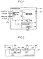
- Fig. 1 is a block diagram showing an example of a configuration of a processor chip for realizing a first embodiment of the present invention.
- a processor chip 101 is an LSI having a circuit of a CMOS structure, and includes a processor main circuit 102, an operation mode control unit 103, and a substrate bias switching unit 104.
- a substrate bias switching unit 104 To the substrate bias switching unit 104, voltages Vdd and Vss in the normal mode, and voltages Vddb and Vssb in the stand-by mode are inputted through a signal 110.
- the substrate bias switching unit 104 selects, as the substrate bias for a p-channel MOS transistor constituting the processor main circuit 102, between Vdd and Vddb to output the selected one to a signal Vbp 111, and also selects, as the substrate bias for an n-channel MOS transistor, between Vss and Vssb to output the selected one to a signal Vbn 112.
- Vdd 1.5V
- Vddb 3.0V
- Vss 0.0V
- Vssb -1.5V.
- a well 302 on which the processor main circuit 102 is formed is formed separately, independently of wells on which the substrate bias switching unit 104 and the operation mode control unit are respectively formed.
- Fig. 3 is a cross sectional view showing a device structure of the processor chip 101.
- a point of difference of Fig. 3 from Fig. 2 is that a p type well 302 is formed in an n type substrate 301 and the n type well 205 is formed in a part of the surface layer of the p type well 302, i.e., the device has a triple well structure.
- An n-channel MOS transistor is formed on the surface of the p type well 302 and a p-channel MOS transistor is formed on the surface of the n type well 205, thereby to constitute a CMOS circuit.
- Vbp 209 is provided in the n type well 205 of the p-channel MOS transistor and Vbn 210 is provided in the p type well 302 of the n-channel MOS transistor is the same as in Fig. 2.
- the processor main circuit 102 is formed in the p type well 302 different from those of the operation mode control unit 103 and the substrate bias switching unit 104.
- the substrate bias control influences only the processor main circuit 102, and hence both the operation mode control unit 103 and the substrate bias switching unit 104 can avoid that influence.
- Fig. 4 is a flow chart showing the processing on the processor chip 101 in the case where the operation mode of the processor main circuit 102 is changed from the normal mode to the stand-by mode and then is changed from the stand-by mode to the normal mode.
- the processor main circuit 102 is operated in the normal mode.
- the sub-strate bias switching unit 104 selects Vdd and Vss for the substrate biases Vbp 111 and Vbn 112, respectively.
- the processor main circuit 102 After the processor main circuit 102 outputs, after having executed the sleep instruction, "stand-by request" to the signal 105 and then informs the operation mode control unit 103 of this fact, the processor main circuit 102 stops the operation of executing the instruction and then proceeds to the stand-by mode (Step 402).
- the operation mode control unit 103 detects that when the processor main circuit 102 is in the stand-by state, "stand-by release interruption" is asserted from the outside to a signal 108 (Step 405), the unit 103 outputs the signal 107 in order for the substrate biases of the processor main circuit 102 to be switched over to the voltages for the normal mode. Then, in response to the signal 107, the substrate bias switching unit 104 switches the substrate biases Vbp 111 and Vbn 112 over to Vdd (1.5V) and Vss (0.0V), respectively (Step 406).
- the operation mode control unit 103 sets a sufficient time period required for stabilization of the substrate bias voltages switched thereto in an on-chip timer 109 and then restarts the processor main circuit 102 (Step 407) and then waits until time-out (Step 408). Then, after time-out, the operation mode control unit 103 outputs "stand-by release" to the signal 106 and then informs the processor main circuit 102 of this fact. In response to the signal 106, the processor main circuit 102 proceeds to the normal mode and restarts the operation of executing an instruction (Step 409).
- the substrate biases Vbp 111 and Vbn 112 of the processor main circuit 102 are controlled such that during the operation, the threshold voltages of the MOS transistors constituting the processor main circuit are decreased to cope with the high speed operation, while during the stand-by, the threshold voltages thereof are increased to able to reduce the leakage current.
- Fig. 5 is a block diagram showing a configuration of the processor chip in a second embodiment of the present invention.
- the operation mode control unit 103 includes a sensor 501 for detecting the bias voltages which are applied to the substrate of the processor main circuit 102.
- the processing procedure in the above-mentioned first embodiment is applied to the present embodiment.
- the operation mode control unit 103 outputs "stand-by release" to the signal 106 in order to restart the operation of the processor main circuit 102.
- Fig. 6 is a block diagram showing a configuration of a processor chip in a third embodiment of the present invention.
- the processor main circuit includes a CPU 604, and a plurality of functional modules such as a module A 606 and a module B 608.
- the functional modules are present separately on the respective different well regions and hence one functional module is not influenced by the substrate bias control for other functional modules.
- the functional module includes the elements, each having the smaller scale unit, such as a CPU, an FPU, a cache, or a computing element.
- Substrate bias switching units 605, 607 and 609 are respectively provided so as to correspond to the functional modules 604, 606 and 608, and can switch, similarly to the above-mentioned embodiments, the substrate biases of the corresponding functional modules.
- the execution of the instruction is carried out with the CPU, as one of the functional modules, as a center, and hence if any instruction to make stand-by any unnecessary functional module for execution is executed, then the operation mode control unit 602 is informed of that the functional module of interest is in the stand-by state.
- the description will hereinbelow be given with respect to the operation of the processor chip 601 in the present embodiment.
- the CPU 604 After having executed the instruction to make stand-by the module A, the CPU 604 outputs the stand-by request to a signal 610, and thereafter, it is impossible to use that module until the stand-by of the module A 606 is released.
- the operation mode control unit 602 After having received the signal 610, the operation mode control unit 602 outputs a signal 612 to the substrate bias switching unit 607 and then switches the substrate biases of the module A 606 over to the voltages for the stand-by mode.
- the unit 602 When the module A 606 is in the stand-by state, after the operation mode control unit 602 has received the signal 610 from the CPU 604 or a signal relating to the stand-by release of the module A 606 from the signal 613 outside of the processor chip 601, the unit 602 outputs the signal 612 to the substrate bias switching unit 607 and then switches the substrate biases of the module A over to the voltages for the normal mode. Then, similarly to the first embodiment of the present invention, the operation mode control unit 602 waits the stabilization of the substrate biases switched thereto using an on-chip timer 603, and after the stabilization thereof, informs the CPU 604 through a signal 611 of that the stand-by of the module A is released. After the CPU 604 has received this signal 611, it becomes possible to execute the instruction using the module A.
- the foregoing is applied to the stand-by control for the module B 608 as well as other functional modules.
- the CPU 604 itself is an object of the stand-by control.
- the functional module B 608 and other functional modules are controlled similarly to the case of the above-mentioned module A 604 except that after having proceeded to the stand-by mode, the CPU 604 stops all the instructions from being executed, and when the signal relating to the stand-by release of the CPU 604 has been asserted to the external signal 613, the operation mode control unit 602 asserts the stand-by release of the CPU 604 to the signal 611 after completion of the switching of the substrate biases of the CPU 604, thereby restarting the execution of the instructions of the CPU 604.
- Fig. 7 is a block diagram showing a configuration of a processor chip in a fourth embodiment of the present invention.
- a point of difference of the present embodiment from the first embodiment is that voltages 701 which are supplied from the outside to the substrate bias switching unit 104 are increased in kind so that the substrate bias switching unit 104 can select, as the substrate biases, the suitable voltages among these voltages 701 to apply them to the processor main circuit 102.
- Vdd for the p-channel MOS transistor
- Vss for the n-channel MOS transistor
- Vddb2 for the p-channel MOS transistor
- Vssb2 for the n-channel MOS transistor
- Vddb1 for the p-channel MOS transistor
- Vssb1 for the n-channel MOS transistor
- the operation mode of the processor main circuit 102 is switched from the high speed mode over to the low speed mode. While the processor main circuit 102 is being operated in the high speed mode, as the substrate biases for the processor main circuit, the substrate switching unit 104 selects Vdd and Vss for Vbp 111 and Vbn 112, respectively. After having executed the instruction to proceed to the low speed mode, the processor main circuit 102 outputs this request to the signal 105 to suspend the operation of executing the instruction. A clock which is supplied to the processor main circuit 102 is switched over to a low frequency on the basis of execution of the instruction to proceed to the low speed mode.
- the operation mode control unit 103 After having received the signal 105, the operation mode control unit 103 outputs the signal 107 in order to switch the substrate biases of the processor main circuit 102 over to the voltages for the low speed mode. In response to the signal 107, the substrate bias switching unit 104 switches the substrate biases Vbp 111 and Vbn 112 over to Vddb2 and Vssb2, respectively. Similarly to the above-mentioned embodiments, the operation mode control unit 103 maintains the stability of the substrate biases switched thereto using the on-chip timer 109, and informs the processor main circuit 102 through the signal 106 of that the proceeding to the low speed mode has been completed. After having received the signal 106, the processor main circuit 102 restarts the suspended operation of executing the instruction in the low speed mode.
- the operation in switching the operation mode from the low speed mode to the high speed mode, in switching the operation mode from the high speed mode or the low speed mode to the stand-by mode, or in switching the operation mode from the stand-by mode to the high speed mode or the low speed mode in the present embodiment is also similar to the foregoing, the details thereof will be omitted here.
- the operation speed is further subdivided and the substrate bias control corresponding thereto is carried out.
- the processor main circuit 102 is separated in functional modules by utilizing the triple well structure of the device, and for every functional module, the substrate biases are controlled in conjunction with the switching of the operation frequency thereof.
- the substrate bias control which is suitable for the operation frequency of the processor is carried out, whereby it is possible to reduce the leakage current in the low speed operation mode.
- the range of the input voltages by which both the p-channel MOS transistor and the n-channel MOS transistor of the CMOS circuit are caused to conduct at the same time is narrower than that in the high speed operation mode, there is also provided the effect that the passing through current during the switching is reduced.
- Fig. 8 is a block diagram showing a configuration of a processor chip in a fifth embodiment of the present invention.
- the above-mentioned substrate bias switching unit is constituted by a substrate bias generating unit 801.
- the substrate bias generating circuit 801 is controlled by an output signal 802 of the operation mode control unit 103 so that it generates in the inside the voltages of the substrate biases to output these voltages to Vbp 111 and Vbn 112, respectively.
- the voltage values of the substrate biases Vbp 111 and Vbn 112 which are generated in correspondence to the operation mode of the processor main circuit 102 under the control by the operation mode control unit 103 are the same values as those in the first embodiment.
- the substrate bias switching unit in the second, third and fourth embodiments is constituted by the substrate bias generating circuit 801, whereby the substrate biases can be generated in the inside of the processor chip to switch the substrate biases thus generated in accordance with the operation mode.
- the optimal substrate bias control corresponding to the operation mode of the processor becomes possible.
- the leakage current can be reduced in the stand-by mode while maintaining the high speed when the operation mode of the processor is the normal mode.
- the substrate bias control is carried out in accordance with the operation mode by the functional module, whereby even when the processor is in operation, the leakage current of any functional module which is unnecessary for the execution can be reduced.
- the substrate bias control which is suitable for the operation frequency of the processor is carried out, whereby in addition to the reduction of the leakage current in the low speed mode, there is also obtained the effect that the passing through current in the switching can be reduced.
- the operation mode in which the substrate biases are controlled will be described concretely.
- the microcomputer has two power sources, i.e., a 1.8V power source and a 3.3V power source, and the substrate bias control is carried out by only the 1.8V power source.
- the circuit for supplying 1.8V is constituted by a MOS transistor having a relative low threshold (e.g., Vth ⁇ 0.4V or so).
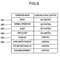
- Fig. 9 shows one example of the operation modes of the microcomputer.
- the operation modes are classified into a normal operation mode 981 in which the microcomputer is normally operated, and a reset mode 982.
- the modes in each of which the microcomputer is operated with the low power consumption are classified into a sleep mode 983, a deep sleep mode 984, a stand-by mode 985, a hardware stand-by mode 986, and an RTC (real time clock) battery back-up mode.
- the test mode there is an IDDQ measurement.
- the RTC battery back-up mode is a mode wherein the voltage from only the power source for the RTC circuit operating at 3.3V is supplied.
- the substrate bias control is carried out.
- the IDDQ measurement is a mode wherein the stand-by current is measured to measure the passing through current due to the short-circuit or the failure of the transistor, in this case, it is required that the substrate biases are necessarily controlled so as to reduce the leakage electric power of the chip to make the discovery of the failure easy.
- FIG. 10 This figure is one example of the main constituent blocks of the processor main circuit.
- computing circuits there are a CPU (central computing processing unit) 971 and an FPU (floating-point computing unit) 972.
- a cache 973 as a memory self contained in the chip, a BSC (bus control unit) 974 for carrying out the interface with an external memory, a DMAC (DMA control unit) 975 for carrying out the DMA (direct memory access), an SCI (serial control unit) 976 for controlling a serial port, an INTC (interruption control unit) 977 for controlling an interruption input, a CPG (clock control unit) 978 for controlling a clock, and the like.
- a BSC bus control unit
- DMAC DMA control unit
- SCI serial control unit
- INTC interruption control unit
- CPG clock control unit
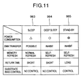
- the sleep 983 only the clock for the computing units such as the CPU 971, the FPU 972, and the cache 973 is stopped and also the substrate bias control is not carried out. Therefore, though the power consumption can not be greatly reduced, the DMA transfer through the DMAC 975, and the normal refresh (refresh at the rate of 102 times/16 msec.) for the DRAM (dynamic RAM) and the SDRAM (synchronous dynamic RAM) through the BSC 974 are possible. Since the CPG 978 is in operation and the substrate bias control is not carried out, the time period required for return from the sleep 983 to the normal operation mode 982 is short.
- the power consumption is very small. Also, since all the clocks are stopped, it is impossible to carry out the DMA transfer.
- the control signals (RAS signal, CAS signal) for the memories are set using the BSC 974 in such a way that before entering into the stand-by 985, the mode becomes the self-refresh mode wherein the memories carry out the refresh by themselves. But, the time period required for return from the stand-by 985 to the normal operation 982 becomes long due to waiting for stability of the clock oscillation and a lapse of the time period required for return from the substrate biasing state since all the clocks are stopped.
- the deep sleep 984 mode is the low power consumption mode between the sleep 983 and the stand-by 985.
- the DMA transfer can not be carried out and also the refresh of the memories becomes the self-refresh.
- the time period required for return from the deep sleep 984 to the normal operation 982 is, similarly to the sleep mode, short.
- the three kinds of low power consumption modes are provided, whereby the fine low power consumption control can be carried out in accordance with the application.
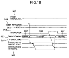
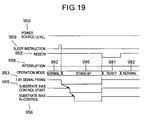
- Fig. 13 shows a state transition diagram of the operation modes in order to give the description thereof.
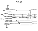
- RESET# 952 or, a power-on reset
- the processor chip makes transition to a reset state 981.
- RESET# 952 is negated
- the processor chip makes transition to the normal operation 982. Then, the processor chip makes transition from this state to the low power consumption operation mode.
- One transition method is the transition based on an instruction.
- the CPU 971 executes a sleep instruction, thereby making this transition.
- a mode register is set in executing the sleep instruction, whereby the selection can be made among the sleep 983, the deep sleep 984 and the stand-by 985, and the processor chip can make transition to the selected one of these modes.
- the return from each of these modes to the normal operation mode 982 is carried out on the basis of an instruction 958.
- the other transition method is the transition based on a HARDSTB# 951 pin.
- the processor chip When having asserted this pin, the processor chip makes transition to a hardware stand-by state 986.
- This state is a state wherein similarly to the stand-by 985, all the clocks are stopped and also the substrate bias control is carried out too.
- Fig. 14 shows configurations of a processor chip 901 and a power source control circuit in which the hardware stand-by is applied to enable a power source (battery) 904 of the processor chip 901 to be exchanged.
- the processor chip 901 is constituted by a 1.8V region circuit 930 which is operated at 1.8V and a 3.3V region circuit 931 which is operated at 3.3V.
- the 1.8V region circuit 930 includes a processor main circuit 902, and level-down circuits 905 and 906 each of which carries out the level conversion from 3.3V down to 1.8V.
- the 3.3V region circuit 931 includes a substrate bias generating circuit 903, a clock oscillation circuit 908, an I/O circuit 909, an operation mode control unit 913, an RTC circuit 914, level-up circuits 904 and 910 each of which carries out the level conversion from 1.8V up to 3.3V, and output fixing circuits 907 and 911 each of which fixes a signal from 3.3V to 1.8V.
- a control circuit for a power source system includes a power source 904, a power source monitoring circuit 921, a display 921, and a voltage producing circuit 920 for producing a voltage for a 1.8V system.
- the substrate bias generating circuit 903 holds the normal substrate levels (e.g., the electric potential VDD for the p-channel MOS transistor, and the electric potential VSS for the n-channel MOS transistor) without carrying out the subtraction with respect to the substrate biases.
- the clock generating circuit 908 includes a PLL (phase-locked loop) and the like, and produces a clock for the internal operation to send it to the processor main circuit 902 through the output fixing circuit 907 and the level-down circuit 905.
- the I/O circuit 909 fetches in a signal from the outside to send it to the processor main circuit 902 through the output fixing circuit 907 and the level-down circuit 905.
- the I/O circuit 909 outputs a signal from the processor main circuit 902 to the outside through the level-up circuit 904.
- the RTC circuit 914 is operated at 3.3V, and receives a control signal from the processor main circuit 902 through the level-up circuit 910 to transmit a control signal to the processor main circuit 902 through the level-down circuit 906 and the output fixing circuit 911.
- the operation mode control unit 913 carries out, in particular, the control for the substrate bias generating circuit 903.
- the power source monitoring circuit 921 monitors the voltage level of the power source 904. When the voltage level has been decreased down to a level lower than a predetermined level (When having detected the exhaustion state of the battery), the circuit 921 makes HARDSTB# 951 the low level. At the same time, the circuit 921 displays the alarm for the battery exhaustion on the display 922 to inform a user of this fact. Even in the state in which the voltage level has been decreased, the voltage holding circuit 923 can hold the voltage level for a predetermined time period (ranging from several minutes to several hours). For this time period, a user can exchange the power source.
- Fig. 16 shows an example of a configuration of realizing the RTC power source back-up mode.
- the RTC circuit 914 is called a real time counter and is provided for realizing the function such as a clock or a calendar. For this reason, the function of a clock can not be realized if the circuit 914 is not operated at all times. Even if the power source 904 is shut-off, the RTC circuit 914 needs to be operated.
- the 3.3V region is divided into a normal 3.3V region 991 and a region 992 in which the associated circuits are operated at 3.3V of the RTC.
- both an input fixing circuit 912 and an input fixing level-up circuit 960 are added to the input circuit so that even when in the state in which other power sources (1.8V, the normal 3.3V power source) are shut-off, the input signal becomes at floating, the signal of an intermediate level is not transmitted to the region 992 in which the associated circuits are operated at 3.3V of the RTC. In such a way, the malfunction is prevented.
- the control circuit for the power source system includes a back-up battery 962, and diodes 963 and 964 in addition to the power source 904, the power source monitoring circuit 921, the display 922, and the voltage producing circuit 920 for producing the voltage of 1.8V system.
- the substrate bias generating circuit 903 holds the normal substrate levels without carrying out the subtraction with respect to the substrate biases.
- the clock oscillation circuit 908 includes a PLL (phased-locked loop) and the like, and produces a clock for the internal operation to send it to the processor main circuit 902 through both the output fixing circuit 907 and the level-down circuit 905.
- the I/O circuit 909 fetches in the signal from the outside and sends the signal thus fetched in to the processor main circuit 902 through both the output fixing circuit 907 and the level-down circuit 905.
- the circuit 909 outputs the signal from the processor main circuit 902 to the outside through the level-up circuit 904.
- the RTC circuit 914 is operated at 3.3V and receives the control signal from the processor main circuit 902 via the input fixing level-up circuit 960 to transmit the control signal to the processor main circuit 902 via both the level-down circuit 906 and the output fixing circuit 911.
- the operation mode control unit 913 receives the control signal via the input fixing circuit 912 to in particular carry out the control for the substrate bias generating circuit 903.
- the voltage monitoring circuit 921 monitors the voltage level of the power source 904. When the voltage level has been decreased down to a level lower than a predetermined level (When having detected the state in which the battery is exhausted up), the circuit 921 makes HARDSTB# 951 a low level, and fixes the inputs to the RTC 3.3V region 992 to prevent the malfunction of the RTC circuit 914. At the same time, the circuit 921 displays the alarm of exhaustion of the battery on the display 922. Thereafter, the voltage level continues to be decreased so that the voltages of 3.3V and 1.8V systems will not be supplied to the processor chip 901.
- the voltages (VDD - RTC, VSS - RTC) are supplied to only the 3.3V region of the RTC from the back-up battery 962 via the diode 963, and hence even when the power source 904 is exhausted up, only the RTC circuit (the counter circuit for a calendar) 914 is normally operated.
- the diode 964 serves to prevent the current from being caused to flow through the circuits other than the RTC circuit 914.
- a power source switch is provided in the power source 904 so that for a time period when the power source is turned off, only the RTC circuit 914 can be operated.
- the processor chip 901 enters into the low power consumption mode and also can return thereto by the interruption.
- the processor chip 901 enters into the low power consumption mode and also can return thereto by the reset.
- the processor chip 901 has a section to which 1.8V is supplied as the power source voltage, and a section to which 3.3V is supplied as the power source voltage.
- the section to which 1.8V is supplied includes the processor main circuit 902 and the like for example.
- This section is a section wherein the circuit scale is large and the high speed operation is required. Since the circuit scale is large and also the high speed operation is required, the power consumption in this section becomes large. In the present embodiment, the power source voltage is reduced in order to reduce that power consumption.
- the substrate voltage control is carried out in order to reduce the sub-threshold leakage current due to the decrease of the threshold voltage.
- the section to which 3.3V is supplied as the power source voltage includes the RTC circuit 914 and the like for example. Since these circuits are small in scale and are operated at the low speed, the power consumption is small. Therefore, for such circuit blocks, the power source voltage does not need to be decreased. For example, the relation of Vth > 0.5V or so can be established. Thus, since the threshold voltage of the MOS transistor does not need to be decreased, there is obtained the advantage that the current measure by the substrate control is not required in order to reduce the sub-threshold leakage current.
- the I/O circuit 909 needs to transmit/receive the external signal amplitude of 3.3V, if the MOS transistor which is the same as the MOS transistor having the high threshold voltage is employed therefor, then the process can be desirably made common thereto.
Landscapes
- Engineering & Computer Science (AREA)
- Theoretical Computer Science (AREA)
- Physics & Mathematics (AREA)
- General Engineering & Computer Science (AREA)
- General Physics & Mathematics (AREA)
- Semiconductor Integrated Circuits (AREA)
- Microcomputers (AREA)
- Logic Circuits (AREA)
Applications Claiming Priority (3)
| Application Number | Priority Date | Filing Date | Title |
|---|---|---|---|
| JP31038096 | 1996-11-21 | ||
| JP31038096 | 1996-11-21 | ||
| PCT/JP1997/004253 WO1998022863A1 (fr) | 1996-11-21 | 1997-11-21 | Processeur a faible consommation d'energie |
Publications (2)
| Publication Number | Publication Date |
|---|---|
| EP0943978A1 true EP0943978A1 (fr) | 1999-09-22 |
| EP0943978A4 EP0943978A4 (fr) | 2006-08-23 |
Family
ID=18004560
Family Applications (1)
| Application Number | Title | Priority Date | Filing Date |
|---|---|---|---|
| EP97913423A Withdrawn EP0943978A4 (fr) | 1996-11-21 | 1997-11-21 | Processeur a faible consommation d'energie |
Country Status (7)
| Country | Link |
|---|---|
| US (4) | US6715090B1 (fr) |
| EP (1) | EP0943978A4 (fr) |
| JP (1) | JP3851663B2 (fr) |
| KR (1) | KR100484699B1 (fr) |
| CN (3) | CN1270223C (fr) |
| TW (1) | TW382670B (fr) |
| WO (1) | WO1998022863A1 (fr) |
Cited By (2)
| Publication number | Priority date | Publication date | Assignee | Title |
|---|---|---|---|---|
| WO2004109531A3 (fr) * | 2003-06-10 | 2005-01-20 | Koninkl Philips Electronics Nv | Commande adaptative en temps reel assurant une meilleure performance de circuits integres |
| US11177792B2 (en) | 2010-08-06 | 2021-11-16 | Semiconductor Energy Laboratory Co., Ltd. | Power supply semiconductor integrated memory control circuit |
Families Citing this family (50)
| Publication number | Priority date | Publication date | Assignee | Title |
|---|---|---|---|---|
| JP3904244B2 (ja) * | 1993-09-17 | 2007-04-11 | 株式会社ルネサステクノロジ | シングル・チップ・データ処理装置 |
| TW382670B (en) * | 1996-11-21 | 2000-02-21 | Hitachi Ltd | Low power processor |
| US6732280B1 (en) * | 1999-07-26 | 2004-05-04 | Hewlett-Packard Development Company, L.P. | Computer system performing machine specific tasks before going to a low power state |
| US6611918B1 (en) * | 1999-12-21 | 2003-08-26 | Intel Corporation | Method and apparatus for changing bias levels to reduce CMOS leakage of a real time clock when switching to a battery mode of operation |
| WO2002061591A1 (fr) * | 2001-01-31 | 2002-08-08 | Hitachi,Ltd | Systeme de traitement de donnees et processeur de donnees |
| KR100424484B1 (ko) * | 2001-07-05 | 2004-03-24 | 엘지전자 주식회사 | 중앙 처리 장치용 전원 공급기 |
| US7051218B1 (en) * | 2001-07-18 | 2006-05-23 | Advanced Micro Devices, Inc. | Message based power management |
| JP3981539B2 (ja) * | 2001-08-28 | 2007-09-26 | Necエレクトロニクス株式会社 | 半導体集積回路装置 |
| US6982500B2 (en) * | 2002-03-11 | 2006-01-03 | Intel Corporation | Power-down scheme for an on-die voltage differentiator design |
| US6920574B2 (en) | 2002-04-29 | 2005-07-19 | Apple Computer, Inc. | Conserving power by reducing voltage supplied to an instruction-processing portion of a processor |
| JP4052923B2 (ja) | 2002-10-25 | 2008-02-27 | 株式会社ルネサステクノロジ | 半導体装置 |
| US7080268B2 (en) * | 2002-12-03 | 2006-07-18 | Intel Corporation | Method and apparatus for regulating power to electronic circuits |
| US7949864B1 (en) * | 2002-12-31 | 2011-05-24 | Vjekoslav Svilan | Balanced adaptive body bias control |
| AU2003217641A1 (en) * | 2003-02-20 | 2004-09-17 | International Business Machines Corporation | Integrated circuit testing methods using well bias modification |
| US7236044B2 (en) * | 2003-10-14 | 2007-06-26 | The Board Of Trustees Of The Leland Stanford Junior University | Apparatus and method for adjusting the substrate impedance of a MOS transistor |
| JP4549652B2 (ja) * | 2003-10-27 | 2010-09-22 | パナソニック株式会社 | プロセッサシステム |
| JP2005157620A (ja) * | 2003-11-25 | 2005-06-16 | Matsushita Electric Ind Co Ltd | 半導体集積回路 |
| JP4316399B2 (ja) * | 2004-02-18 | 2009-08-19 | インターナショナル・ビジネス・マシーンズ・コーポレーション | プログラム、記録媒体、制御方法、及び情報処理装置 |
| CN100363867C (zh) * | 2004-12-10 | 2008-01-23 | 神基科技股份有限公司 | 中央处理器的省电电路与方法 |
| WO2006075287A2 (fr) * | 2005-01-12 | 2006-07-20 | Nxp B.V. | Procede et appareil permettant d'accorder un systeme numerique |
| US7180353B2 (en) * | 2005-02-03 | 2007-02-20 | Mediatek Incorporation | Apparatus and method for low power clock distribution |
| US7486098B2 (en) * | 2005-06-16 | 2009-02-03 | International Business Machines Corporation | Integrated circuit testing method using well bias modification |
| JP4361073B2 (ja) * | 2005-07-28 | 2009-11-11 | 株式会社リコー | 画像処理装置とその制御方法 |
| KR100714426B1 (ko) | 2005-09-05 | 2007-05-07 | 삼성전자주식회사 | 컴퓨터시스템 및 그 전원공급방법 |
| JP4621113B2 (ja) * | 2005-10-28 | 2011-01-26 | ルネサスエレクトロニクス株式会社 | 半導体集積回路装置 |
| JP2007148952A (ja) * | 2005-11-30 | 2007-06-14 | Renesas Technology Corp | 半導体集積回路 |
| US7295036B1 (en) * | 2005-11-30 | 2007-11-13 | Altera Corporation | Method and system for reducing static leakage current in programmable logic devices |
| US7902654B2 (en) * | 2006-05-10 | 2011-03-08 | Qualcomm Incorporated | System and method of silicon switched power delivery using a package |
| JP2008098774A (ja) * | 2006-10-06 | 2008-04-24 | Oki Electric Ind Co Ltd | 半導体集積回路装置 |
| KR101101826B1 (ko) | 2006-10-24 | 2012-01-05 | 삼성전자주식회사 | 화상처리장치 및 화상처리방법 |
| US7779237B2 (en) * | 2007-07-11 | 2010-08-17 | International Business Machines Corporation | Adaptive execution frequency control method for enhanced instruction throughput |
| US7937568B2 (en) * | 2007-07-11 | 2011-05-03 | International Business Machines Corporation | Adaptive execution cycle control method for enhanced instruction throughput |
| US8028181B2 (en) * | 2008-09-19 | 2011-09-27 | Intel Corporation | Processor power consumption control and voltage drop via micro-architectural bandwidth throttling |
| JP4966956B2 (ja) * | 2008-12-22 | 2012-07-04 | 株式会社日立製作所 | 半導体装置 |
| KR101046731B1 (ko) * | 2008-12-26 | 2011-07-05 | 주식회사 하이닉스반도체 | 파워 분배 장치와 그를 갖는 메모리 장치 |
| KR101003153B1 (ko) * | 2009-05-15 | 2010-12-21 | 주식회사 하이닉스반도체 | 전압 안정화 회로 및 이를 이용한 반도체 메모리 장치 |
| JP5488361B2 (ja) * | 2010-09-15 | 2014-05-14 | 富士通株式会社 | 半導体集積回路 |
| TWI582575B (zh) * | 2011-03-17 | 2017-05-11 | 和碩聯合科技股份有限公司 | 電子裝置 |
| US8977878B2 (en) * | 2011-05-19 | 2015-03-10 | Texas Instruments Incorporated | Reducing current leakage in L1 program memory |
| US20130033306A1 (en) * | 2011-08-01 | 2013-02-07 | International Business Machines Corporation | Performance of digital circuits using current management |
| US8945785B2 (en) * | 2012-01-06 | 2015-02-03 | GM Global Technology Operations LLC | Adaptive limitation of standby mode to enhance fuel cell system life |
| US9134777B2 (en) | 2012-06-06 | 2015-09-15 | Qualcomm Incorporated | Bi-modal power delivery scheme for an integrated circuit comprising multiple functional blocks on a single die to achieve desired average throughput for the integrated circuit |
| US9971947B2 (en) * | 2014-07-31 | 2018-05-15 | Magna Electronics Inc. | Vehicle vision system with camera power control |
| JP6582378B2 (ja) * | 2014-09-08 | 2019-10-02 | セイコーエプソン株式会社 | 発振回路、発振器、電子機器及び移動体 |
| US9842182B2 (en) | 2014-10-01 | 2017-12-12 | Samsung Electronics Co., Ltd. | Method and system for designing semiconductor device |
| WO2017019011A1 (fr) * | 2015-07-27 | 2017-02-02 | Hewlett-Packard Development Company, L.P. | Modification d'une image de rastérisation à jet d'encre pour un effet autonome visible |
| CN118069218A (zh) * | 2017-09-12 | 2024-05-24 | 恩倍科微公司 | 极低功率微控制器系统 |
| US10824376B2 (en) | 2017-12-08 | 2020-11-03 | Sandisk Technologies Llc | Microcontroller architecture for non-volatile memory |
| US11892520B2 (en) | 2022-03-28 | 2024-02-06 | Changxin Memory Technologies, Inc. | Method and device for power supply mapping detection, electronic device, and medium |
| CN116859291A (zh) * | 2022-03-28 | 2023-10-10 | 长鑫存储技术有限公司 | 电源映射检测方法、装置、电子设备及介质 |
Family Cites Families (31)
| Publication number | Priority date | Publication date | Assignee | Title |
|---|---|---|---|---|
| US4356412A (en) * | 1979-03-05 | 1982-10-26 | Motorola, Inc. | Substrate bias regulator |
| US4460835A (en) * | 1980-05-13 | 1984-07-17 | Tokyo Shibaura Denki Kabushiki Kaisha | Semiconductor integrated circuit device with low power consumption in a standby mode using an on-chip substrate bias generator |
| US5339446A (en) * | 1986-12-26 | 1994-08-16 | Kabushiki Kaisha Toshiba | Power supply and method for use in a computer system to confirm a save operation of the computer system and to stop a supply of power to the computer system after confirmation |
| US5297097A (en) * | 1988-06-17 | 1994-03-22 | Hitachi Ltd. | Large scale integrated circuit for low voltage operation |
| US5241680A (en) * | 1989-06-12 | 1993-08-31 | Grid Systems Corporation | Low-power, standby mode computer |
| US5167024A (en) * | 1989-09-08 | 1992-11-24 | Apple Computer, Inc. | Power management for a laptop computer with slow and sleep modes |
| US5111058A (en) * | 1990-05-23 | 1992-05-05 | Martin Richard A | Circuit for sustaining power supply output following momentary interruption of commercial a.c. power |
| JPH0511876A (ja) * | 1990-12-25 | 1993-01-22 | Mitsubishi Electric Corp | デイジタル回路装置 |
| US5652890A (en) * | 1991-05-17 | 1997-07-29 | Vantus Technologies, Inc. | Interrupt for a protected mode microprocessor which facilitates transparent entry to and exit from suspend mode |
| JP3184265B2 (ja) | 1991-10-17 | 2001-07-09 | 株式会社日立製作所 | 半導体集積回路装置およびその制御方法 |
| US5410713A (en) * | 1992-01-02 | 1995-04-25 | Smith Corona/Acer | Power-management system for a computer |
| EP0836194B1 (fr) * | 1992-03-30 | 2000-05-24 | Mitsubishi Denki Kabushiki Kaisha | Dispositif à semi-conducteurs |
| JP2939086B2 (ja) | 1992-03-30 | 1999-08-25 | 三菱電機株式会社 | 半導体装置 |
| US5461338A (en) * | 1992-04-17 | 1995-10-24 | Nec Corporation | Semiconductor integrated circuit incorporated with substrate bias control circuit |
| JP3503961B2 (ja) | 1992-06-02 | 2004-03-08 | 株式会社東芝 | 半導体装置 |
| JP2888722B2 (ja) * | 1993-04-12 | 1999-05-10 | 株式会社東芝 | インターフェース回路 |
| US6031411A (en) * | 1993-06-28 | 2000-02-29 | Texas Instruments Incorporated | Low power substrate bias circuit |
| US5442794A (en) * | 1993-12-01 | 1995-08-15 | Advanced Micro Devices, Inc. | Disable technique employed during low battery conditions within a portable computer system |
| JPH07254685A (ja) * | 1994-03-16 | 1995-10-03 | Toshiba Corp | 半導体記憶装置 |
| JP2822881B2 (ja) * | 1994-03-30 | 1998-11-11 | 日本電気株式会社 | 半導体集積回路装置 |
| US5587916A (en) * | 1994-08-15 | 1996-12-24 | B.E.L.-Tronics Limited | Low voltage sensing circuits for battery powered devices having a micro-processor |
| JP3645593B2 (ja) * | 1994-09-09 | 2005-05-11 | 株式会社ルネサステクノロジ | 半導体集積回路装置 |
| US5633573A (en) * | 1994-11-10 | 1997-05-27 | Duracell, Inc. | Battery pack having a processor controlled battery operating system |
| EP0714099A1 (fr) * | 1994-11-24 | 1996-05-29 | STMicroelectronics S.r.l. | Circuit intégré CMOS pour alimentation à faible énergie et ayant une faible dissipation d'énergie en stand-by |
| US5778237A (en) * | 1995-01-10 | 1998-07-07 | Hitachi, Ltd. | Data processor and single-chip microcomputer with changing clock frequency and operating voltage |
| JP3175521B2 (ja) | 1995-01-27 | 2001-06-11 | 日本電気株式会社 | シリコン・オン・インシュレータ半導体装置及びバイアス電圧発生回路 |
| US6640255B1 (en) * | 1995-03-31 | 2003-10-28 | Sun Microsystems, Inc. | Method and apparatus for generation and installation of distributed objects on a distributed object system |
| US5721935A (en) * | 1995-12-20 | 1998-02-24 | Compaq Computer Corporation | Apparatus and method for entering low power mode in a computer system |
| US5812860A (en) * | 1996-02-12 | 1998-09-22 | Intel Corporation | Method and apparatus providing multiple voltages and frequencies selectable based on real time criteria to control power consumption |
| US5917365A (en) * | 1996-04-19 | 1999-06-29 | Texas Instruments Incorporated | Optimizing the operating characteristics of a CMOS integrated circuit |
| TW382670B (en) * | 1996-11-21 | 2000-02-21 | Hitachi Ltd | Low power processor |
-
1997
- 1997-11-20 TW TW086117369A patent/TW382670B/zh not_active IP Right Cessation
- 1997-11-21 EP EP97913423A patent/EP0943978A4/fr not_active Withdrawn
- 1997-11-21 US US09/308,488 patent/US6715090B1/en not_active Expired - Lifetime
- 1997-11-21 CN CNB031075541A patent/CN1270223C/zh not_active Expired - Fee Related
- 1997-11-21 KR KR10-1999-7004444A patent/KR100484699B1/ko not_active Expired - Fee Related
- 1997-11-21 CN CN97199916A patent/CN1122906C/zh not_active Expired - Fee Related
- 1997-11-21 JP JP52347998A patent/JP3851663B2/ja not_active Expired - Lifetime
- 1997-11-21 WO PCT/JP1997/004253 patent/WO1998022863A1/fr not_active Ceased
-
2003
- 2003-03-27 CN CN03107553A patent/CN1442768A/zh active Pending
-
2004
- 2004-02-02 US US10/768,136 patent/US7475261B2/en not_active Expired - Fee Related
-
2008
- 2008-12-30 US US12/346,268 patent/US7958379B2/en not_active Expired - Fee Related
-
2011
- 2011-05-05 US US13/101,678 patent/US8364988B2/en not_active Expired - Fee Related
Cited By (6)
| Publication number | Priority date | Publication date | Assignee | Title |
|---|---|---|---|---|
| WO2004109531A3 (fr) * | 2003-06-10 | 2005-01-20 | Koninkl Philips Electronics Nv | Commande adaptative en temps reel assurant une meilleure performance de circuits integres |
| US7500204B2 (en) | 2003-06-10 | 2009-03-03 | Nxp B.V. | Real-time adaptive control for best IC performance |
| US11177792B2 (en) | 2010-08-06 | 2021-11-16 | Semiconductor Energy Laboratory Co., Ltd. | Power supply semiconductor integrated memory control circuit |
| US11677384B2 (en) | 2010-08-06 | 2023-06-13 | Semiconductor Energy Laboratory Co., Ltd. | Semiconductor integrated circuit with semiconductor layer having indium, zinc, and oxygen |
| US12021530B2 (en) | 2010-08-06 | 2024-06-25 | Semiconductor Energy Laboratory Co., Ltd. | Semiconductor integrated circuit |
| US12273109B2 (en) | 2010-08-06 | 2025-04-08 | Semiconductor Energy Laboratory Co., Ltd. | Semiconductor integrated circuit |
Also Published As
| Publication number | Publication date |
|---|---|
| JP3851663B2 (ja) | 2006-11-29 |
| US7475261B2 (en) | 2009-01-06 |
| US20100005324A1 (en) | 2010-01-07 |
| CN1238047A (zh) | 1999-12-08 |
| KR100484699B1 (ko) | 2005-04-22 |
| US8364988B2 (en) | 2013-01-29 |
| CN1442768A (zh) | 2003-09-17 |
| KR20000057158A (ko) | 2000-09-15 |
| TW382670B (en) | 2000-02-21 |
| CN1270223C (zh) | 2006-08-16 |
| WO1998022863A1 (fr) | 1998-05-28 |
| US20110208983A1 (en) | 2011-08-25 |
| US6715090B1 (en) | 2004-03-30 |
| CN1122906C (zh) | 2003-10-01 |
| EP0943978A4 (fr) | 2006-08-23 |
| US20040158756A1 (en) | 2004-08-12 |
| US7958379B2 (en) | 2011-06-07 |
| CN1442769A (zh) | 2003-09-17 |
Similar Documents
| Publication | Publication Date | Title |
|---|---|---|
| US6715090B1 (en) | Processor for controlling substrate biases in accordance to the operation modes of the processor | |
| JPWO1998022863A1 (ja) | 低電力プロセッサ | |
| US6367021B1 (en) | Power management system with programable configuration circuitry using digital power level signal to selectively configure operations of electronic circuits | |
| US6347379B1 (en) | Reducing power consumption of an electronic device | |
| US9471121B2 (en) | Microprocessor based power management system architecture | |
| US7181188B2 (en) | Method and apparatus for entering a low power mode | |
| CA2210024C (fr) | Methode et appareil de commutation d'alimentation electrique avec protection de l'integrite logique | |
| US7370216B2 (en) | Conserving power by reducing voltage supplied to an instruction-processing portion of a processor | |
| US8736314B2 (en) | Leakage power management using programmable power gating transistors and on-chip aging and temperature tracking circuit | |
| US20030218494A1 (en) | Method of setting back bias of MOS circuit, and MOS integrated circuit | |
| US5844435A (en) | Low power, high accuracy clock circuit and method for integrated circuits | |
| US5842028A (en) | Method for waking up an integrated circuit from low power mode | |
| JP4521619B2 (ja) | 低電力プロセッサ | |
| US10664006B2 (en) | Method and apparatus for automatic switch to retention mode based on architectural clock gating | |
| CN112235850A (zh) | 一种物联网芯片的低功耗系统及方法 | |
| US7516347B2 (en) | Electronic device having power-down mode and method of reducing power consumption | |
| JP4387122B2 (ja) | 低電力プロセッサ | |
| JPWO2000045437A1 (ja) | Mos回路のバックバイアス設定方法とmos集積回路装置 |
Legal Events
| Date | Code | Title | Description |
|---|---|---|---|
| PUAI | Public reference made under article 153(3) epc to a published international application that has entered the european phase |
Free format text: ORIGINAL CODE: 0009012 |
|
| 17P | Request for examination filed |
Effective date: 19990614 |
|
| AK | Designated contracting states |
Kind code of ref document: A1 Designated state(s): DE FR GB IT |
|
| A4 | Supplementary search report drawn up and despatched |
Effective date: 20060726 |
|
| 17Q | First examination report despatched |
Effective date: 20061006 |
|
| RAP1 | Party data changed (applicant data changed or rights of an application transferred) |
Owner name: RENESAS ELECTRONICS CORPORATION |
|
| GRAP | Despatch of communication of intention to grant a patent |
Free format text: ORIGINAL CODE: EPIDOSNIGR1 |
|
| RIC1 | Information provided on ipc code assigned before grant |
Ipc: G06F 1/32 20060101AFI20160513BHEP |
|
| INTG | Intention to grant announced |
Effective date: 20160531 |
|
| STAA | Information on the status of an ep patent application or granted ep patent |
Free format text: STATUS: GRANT OF PATENT IS INTENDED |
|
| STAA | Information on the status of an ep patent application or granted ep patent |
Free format text: STATUS: THE APPLICATION IS DEEMED TO BE WITHDRAWN |
|
| 18D | Application deemed to be withdrawn |
Effective date: 20161011 |