EP0944128B1 - Antenne et dispositif radio portable l'utilisant - Google Patents
Antenne et dispositif radio portable l'utilisant Download PDFInfo
- Publication number
- EP0944128B1 EP0944128B1 EP98112066A EP98112066A EP0944128B1 EP 0944128 B1 EP0944128 B1 EP 0944128B1 EP 98112066 A EP98112066 A EP 98112066A EP 98112066 A EP98112066 A EP 98112066A EP 0944128 B1 EP0944128 B1 EP 0944128B1
- Authority
- EP
- European Patent Office
- Prior art keywords
- antenna apparatus
- antenna
- conductor
- base member
- mounting substrate
- Prior art date
- Legal status (The legal status is an assumption and is not a legal conclusion. Google has not performed a legal analysis and makes no representation as to the accuracy of the status listed.)
- Expired - Lifetime
Links
- 239000004020 conductor Substances 0.000 claims description 65
- 239000000758 substrate Substances 0.000 claims description 45
- 239000000919 ceramic Substances 0.000 claims description 4
- 238000003475 lamination Methods 0.000 claims description 4
- 230000005540 biological transmission Effects 0.000 description 7
- VYPSYNLAJGMNEJ-UHFFFAOYSA-N Silicium dioxide Chemical compound O=[Si]=O VYPSYNLAJGMNEJ-UHFFFAOYSA-N 0.000 description 6
- QVQLCTNNEUAWMS-UHFFFAOYSA-N barium oxide Chemical compound [Ba]=O QVQLCTNNEUAWMS-UHFFFAOYSA-N 0.000 description 6
- 230000000694 effects Effects 0.000 description 6
- 239000000203 mixture Substances 0.000 description 6
- 239000003989 dielectric material Substances 0.000 description 5
- 238000010586 diagram Methods 0.000 description 4
- 230000005404 monopole Effects 0.000 description 4
- 230000006866 deterioration Effects 0.000 description 3
- 230000004048 modification Effects 0.000 description 3
- 238000012986 modification Methods 0.000 description 3
- TWNQGVIAIRXVLR-UHFFFAOYSA-N oxo(oxoalumanyloxy)alumane Chemical compound O=[Al]O[Al]=O TWNQGVIAIRXVLR-UHFFFAOYSA-N 0.000 description 3
- 239000000377 silicon dioxide Substances 0.000 description 3
- XEEYBQQBJWHFJM-UHFFFAOYSA-N Iron Chemical compound [Fe] XEEYBQQBJWHFJM-UHFFFAOYSA-N 0.000 description 2
- PXHVJJICTQNCMI-UHFFFAOYSA-N Nickel Chemical compound [Ni] PXHVJJICTQNCMI-UHFFFAOYSA-N 0.000 description 2
- 238000009826 distribution Methods 0.000 description 2
- 230000005684 electric field Effects 0.000 description 2
- 239000000696 magnetic material Substances 0.000 description 2
- PLDDOISOJJCEMH-UHFFFAOYSA-N neodymium(3+);oxygen(2-) Chemical compound [O-2].[O-2].[O-2].[Nd+3].[Nd+3] PLDDOISOJJCEMH-UHFFFAOYSA-N 0.000 description 2
- 238000007650 screen-printing Methods 0.000 description 2
- RYGMFSIKBFXOCR-UHFFFAOYSA-N Copper Chemical compound [Cu] RYGMFSIKBFXOCR-UHFFFAOYSA-N 0.000 description 1
- 229910000881 Cu alloy Inorganic materials 0.000 description 1
- GWEVSGVZZGPLCZ-UHFFFAOYSA-N Titan oxide Chemical compound O=[Ti]=O GWEVSGVZZGPLCZ-UHFFFAOYSA-N 0.000 description 1
- 239000010941 cobalt Substances 0.000 description 1
- 229910017052 cobalt Inorganic materials 0.000 description 1
- GUTLYIVDDKVIGB-UHFFFAOYSA-N cobalt atom Chemical compound [Co] GUTLYIVDDKVIGB-UHFFFAOYSA-N 0.000 description 1
- 238000004891 communication Methods 0.000 description 1
- 229910052802 copper Inorganic materials 0.000 description 1
- 239000010949 copper Substances 0.000 description 1
- 230000008021 deposition Effects 0.000 description 1
- 238000000151 deposition Methods 0.000 description 1
- 229910052742 iron Inorganic materials 0.000 description 1
- 238000010030 laminating Methods 0.000 description 1
- 238000004519 manufacturing process Methods 0.000 description 1
- 238000000034 method Methods 0.000 description 1
- 229910052759 nickel Inorganic materials 0.000 description 1
- 238000007747 plating Methods 0.000 description 1
- 238000007639 printing Methods 0.000 description 1
- OGIDPMRJRNCKJF-UHFFFAOYSA-N titanium oxide Inorganic materials [Ti]=O OGIDPMRJRNCKJF-UHFFFAOYSA-N 0.000 description 1
Images



Classifications
-
- H—ELECTRICITY
- H01—ELECTRIC ELEMENTS
- H01Q—ANTENNAS, i.e. RADIO AERIALS
- H01Q1/00—Details of, or arrangements associated with, antennas
- H01Q1/36—Structural form of radiating elements, e.g. cone, spiral, umbrella; Particular materials used therewith
- H01Q1/362—Structural form of radiating elements, e.g. cone, spiral, umbrella; Particular materials used therewith for broadside radiating helical antennas
-
- H—ELECTRICITY
- H01—ELECTRIC ELEMENTS
- H01Q—ANTENNAS, i.e. RADIO AERIALS
- H01Q1/00—Details of, or arrangements associated with, antennas
- H01Q1/12—Supports; Mounting means
- H01Q1/22—Supports; Mounting means by structural association with other equipment or articles
- H01Q1/24—Supports; Mounting means by structural association with other equipment or articles with receiving set
- H01Q1/241—Supports; Mounting means by structural association with other equipment or articles with receiving set used in mobile communications, e.g. GSM
- H01Q1/242—Supports; Mounting means by structural association with other equipment or articles with receiving set used in mobile communications, e.g. GSM specially adapted for hand-held use
- H01Q1/243—Supports; Mounting means by structural association with other equipment or articles with receiving set used in mobile communications, e.g. GSM specially adapted for hand-held use with built-in antennas
-
- H—ELECTRICITY
- H01—ELECTRIC ELEMENTS
- H01Q—ANTENNAS, i.e. RADIO AERIALS
- H01Q1/00—Details of, or arrangements associated with, antennas
- H01Q1/36—Structural form of radiating elements, e.g. cone, spiral, umbrella; Particular materials used therewith
- H01Q1/38—Structural form of radiating elements, e.g. cone, spiral, umbrella; Particular materials used therewith formed by a conductive layer on an insulating support
-
- H—ELECTRICITY
- H01—ELECTRIC ELEMENTS
- H01Q—ANTENNAS, i.e. RADIO AERIALS
- H01Q11/00—Electrically-long antennas having dimensions more than twice the shortest operating wavelength and consisting of conductive active radiating elements
- H01Q11/02—Non-resonant antennas, e.g. travelling-wave antenna
- H01Q11/08—Helical antennas
Definitions
- the present invention relates to an antenna apparatus and a portable radio device using the same, and more particularly, to an antenna apparatus provided with a radiative conductor and a portable radio device using the same.
- Monopole antennas and loop antennas have been conventionally used for portable radio devices such as a portable telephone and a pager. As portable radio devices have been made compact, antennas are required to be made compact. Since a monopole antenna and a loop antenna need to have a radiative conductor with a length of one-fourth the wavelength of the used signal, however, the antennas become large and a demand for compact antennas cannot be satisfied.
- a chip antenna 50 is provided with a rectangular-parallelepiped base member 51 having a mounting surface 511 and made from dielectric ceramic including barium oxide, aluminum oxide, and silica as its main components. Inside the base member 51, a spirally wound conductor 52 is formed. A power-supply electrode 53 for applying a voltage to the conductor 52 is formed on surfaces of the base member 51. One end of the conductor 52 is drawn to a surface of the base member 51 and connected to the power-supply electrode 53. The other end of the conductor 52 forms a free end 54 inside the base member 51.
- EP 0 831 546 A2 which is a document under Article 54(3) EPC, describes an antenna device comprising an antenna main body and a mounting board, wherein the main body is made of a dielectric material having provided therein a conductor which is connected between a feed terminal and a free terminal of the antenna main body.
- the mounting board On the mounting board, a transmission line connected to the feeding terminal and a capacitor-forming conductor connected to the free terminal of the antenna main body is provided.
- EP 0 749 214 A2 describes a radio communication equipment using a small chip antenna which is formed of a dielectric substrate in which a spirally-wound conductor is provided.
- the dielectric substrate comprises a feed terminal to which one end of the conductor is connected.
- the other end of the conductor is a free end.
- EP 0 743 699 A1 describes an antenna system comprising a dielectric substrate in which a spirally-wound conductor is provided. Further, a power supply terminal is provided to which one end of the conductor is connected. The other end of the conductor is a free end.
- EP 0 621 653 A2 describes a surface-mountable antenna unit including a dielectric substrate which is provided on a side surface and/or a bottom surface thereof with a ground electrode and a radiator provided with a radiating part having a substantially rectangular plane shape which is fixed to the dielectric substrate so that the radiator is opposed to a top surface of the dielectric substrate, with a feed part provided on a side surface of the substrate and the radiator.
- the present invention provides an antenna apparatus including a chip antenna and a mounting substrate on which the chip antenna is mounted, the chip antenna including a base member made of ceramic, a conductor formed on the base member, and a power-supply electrode to which one end of the conductor is connected and a terminal electrode to which the other end of the conductor is connected, both electrodes being formed on a surface of the base member, and the mounting substrate including a radiative conductor and a ground electrode, wherein the terminal electrode of the chip antenna is connected to one end of the radiative conductor of the mounting substrate.
- the mounting substrate is provided with the radiative conductor which is connected to the conductor of the chip antenna, the effective length of the conductor of the antenna apparatus becomes long. Therefore, since the current distribution of the conductor in the antenna apparatus becomes large and the radiative electric field of the antenna apparatus becomes strong, a high gain and a wide bandwidth are obtained at a low resonant frequency.
- the above antenna apparatus may be configured such that a circuit board on which a ground electrode is formed on a surface thereof which is turned away from a surface of the mounting substrate on which the chip antenna is mounted is disposed such that the mounting substrate is substantially parallel to the circuit board, and the ground electrode of the mounting substrate is connected to the ground electrode of the circuit board.
- the current flowing through the antenna apparatus flows into the ground electrode of the circuit board. Therefore, the characteristics of the antenna apparatus are unlikely to be subject to an effect of a ground disposed at the side of the mounting substrate where the chip antenna is not mounted.
- the above antenna apparatus may be configured such that the base member is formed of a laminated member including a plurality of layers; each of the layers having a main surface; the base member having a lamination direction substantially perpendicular to the main surface; and the conductor being formed in a spiral shape and having a spiral axis substantially perpendicular to the lamination direction of the base member.
- the conductor may have a meander shape.
- the present invention also provides a portable radio device including the antenna apparatus described above, a transmitting circuit connected to the antenna apparatus, a receiving circuit connected to the antenna apparatus, and a casing for covering the antenna apparatus, the transmitting circuit, and the receiving circuit.
- the above portable radio device Since the above portable radio device has an antenna apparatus which can have a high gain and a wide bandwidth at a low resonant frequency, it can be used for transmission and receiving in a low frequency region. In addition, since it has an antenna apparatus which is unlikely to be subject to an effect of the ground, deterioration caused by the ground disposed at the side of the mounting substrate where the chip antenna is not mounted, in transmission and receiving of the portable radio device is prevented.
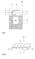
- Fig. 1 is a top view of an antenna apparatus according to a first embodiment of the present invention.
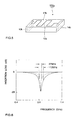
- Fig. 2 is a transparent perspective view of a chip antenna of the antenna apparatus.
- Fig. 3 is an exploded perspective view of the chip antenna shown in Fig. 2 .
- Fig. 4 is a transparent perspective view of a modification of the chip antenna shown in Fig. 2 .
- Fig. 5 is a transparent perspective view of another modification of the chip antenna shown in Fig. 2 .
- Fig. 6 is a view showing a pass characteristic of the antenna apparatus shown in Fig. 1 .
- Fig. 7 is a top view of an antenna apparatus according to a second embodiment of the present invention.
- Fig. 8 is a cross section taken on line VIII-VIII of the antenna apparatus shown in Fig. 7 .
- Fig. 9 is a view showing the directivity of the antenna apparatus shown in Fig. 1 and the directivity of the antenna apparatus shown in Fig. 7 .
- Fig. 10 is an RF block diagram of a portable radio device using an antenna apparatus according to the present invention.
- Fig. 11 is an RF block diagram of another portable radio device using an antenna apparatus according to the present invention.
- Fig. 12 is a transparent perspective view of a conventional chip antenna.
- FIG. 1 is a top view of an antenna apparatus according to a first embodiment of the present invention.
- An antenna apparatus 10 includes a chip antenna 15 provided with a base member 11, a conductor 12 formed in the base member 11, a power-supply electrode 13 to which one end of the conductor 12 is connected, and a terminal electrode 14 to which the other end of the conductor is connected.
- the antenna apparatus 10 further includes a mounting substrate 19 provided with a line-shaped radiative conductor 16 formed by printing an electrically conductive material on a surface thereof, a line-shaped conductive pattern 17, and a substantially rectangular ground electrode 18.
- the chip antenna 15 is mounted on the mounting substrate 19.
- the power-supply electrode 13 of the chip antenna 15 is connected through the conductive pattern 17 on the mounting substrate 19 to a high-frequency circuit RF of a portable radio device on which the antenna apparatus 10 is mounted.
- the terminal electrode 14 of the chip antenna 15 is connected to one end of the radiative conductor 16 on the mounting substrate 19.
- the effective length of the conductor of the antenna apparatus 10 becomes long.
- the chip antenna 15 is provided with the rectangular-parallelepiped base member 11; the conductor 12 spirally wound in the longitudinal direction of the base member 11 inside the base member 11; the power-supply electrode 13 for applying a voltage to the base member 11, which is formed on a surface of the base member 11 and to which one end of the conductor 12 is connected; and the terminal electrode 14 formed on a surface of the base member 11 and to which the other end of the base member 11 is connected.
- Fig. 3 is an exploded perspective view of the chip antenna 15 shown in Fig. 2 .
- the base member 11 is formed by laminating rectangular sheet layers 1a to 1c made of dielectric ceramic including barium oxide, aluminum oxide, and silica as its main components.
- substantially L-shaped or substantially line-shaped electrically conductive patterns 2a to 2g of copper or a copper alloy are provided by screen printing, deposition, or plating.
- Via holes 3 are formed in the thickness direction at specified positions (both ends of the electrically conductive patterns 2e to 2g) of the sheet layer 1b.
- the sheet layers 2a to 2c are laminated, the electrically conductive patterns 2a to 2g are connected to the via holes 3, and the base member is baked to form the conductor 12, which is spirally wound in the longitudinal direction of the base member 11 inside the base member 11.
- One end of the conductor 12 (one end of the electrically conductive pattern 2a) is drawn to one end face having a short edge of the base member 11 and connected to the power-supply electrode 13, provided on a surface of the base member 11.
- the other end of the conductor 11 (one end of the electrically conductive pattern 2d) is drawn to the other end face having a short edge of the base member 11 and connected to the terminal electrode 14, provided on a surface of the base member 11.
- FIGs. 4 and 5 are transparent perspective views of modifications of the chip antenna 15, shown in Fig. 2 .
- a chip antenna 15a shown in Fig. 4 is provided with a rectangular-parallelepiped base member 11a; a conductor 12a spirally wound in the longitudinal direction of the base member 11a along surfaces of the base member 11a; and a power-supply electrode 13a and a terminal electrode 14a formed on surfaces of the base member 11a.
- One end of the conductor 12a is connected to the power-supply electrode 13a for applying a voltage to the conductor 12a on one main surface of the base member 11a, and the other end of the conductor 12a is connected to the terminal electrode 14a on the main surface of the base member 11a.
- the chip antenna 15a configured as described above, since the conductor 12a can be easily formed spirally on surfaces of the base member 11a by screen printing or other methods, the manufacturing process of the chip antenna 15a can be simplified.
- a chip antenna 15b shown in Fig. 5 is provided with a rectangular-parallelepiped base member 11b; a conductor 12b formed on a surface of the base member 11b in a meander shape; and a power-supply electrode 13b and a terminal electrode 14b formed on surfaces of the base member 11b.
- One end of the conductor 12b is connected to the power-supply electrode 13b for applying a voltage to the conductor 12b on one main surface of the base member 11b, and the other end of the conductor 12b is connected to the terminal electrode 14b on the main surface of the base member 11b.
- the base member 11b can be made to have a low profile. Accordingly, the chip antenna 15b can be made to have a low profile.
- the meander-shaped conductor 12b is formed inside the base member 11b, the same advantages are obtained.
- Fig. 6 shows a pass characteristic (dB) of the antenna apparatus 10 ( Fig. 1 ).
- the chip antenna 14 measures 5 mm (width) by 8 mm (depth) by 2.5 mm (height), and the radiative conductor 15 measures 20 mm (width) by 1 mm (depth).
- a solid line corresponds to the antenna apparatus 10 according to the first embodiment, which has the radiative conductor 15, and a dotted line corresponds to the conventional chip antenna 50 ( Fig. 2 ), for comparison.
- the antenna apparatus 10 in a resonant frequency ranging from 930 MHz to 940 MHz, whereas the conventional chip antenna 50 has a bandwidth of 37 MHz and a gain of -4.0 dBd, the antenna apparatus 10 according to the first embodiment has a bandwidth of 113 MHz, which is wider by 76 MHz, and a gain of -3.0 dBd, which is larger by 1.0 dBd.
- a conventional monopole antenna having a resonant frequency of 930 MHz to 940 MHz is about 80 mm long.
- the antenna apparatus 10 according to the first embodiment of the present invention has a length of 22 to 23 mm in the width direction and the length is about one-fourth that of the conventional monopole antenna.
- the antenna apparatus of the above first embodiment since the mounting substrate is provided with the radiative conductor which is connected to the conductor of the chip antenna, the effective length of the conductor of the antenna apparatus becomes long. Therefore, since the current distribution of the conductor in the antenna apparatus becomes large and the radiative electric field of the antenna apparatus becomes strong, a high gain and a wide bandwidth are obtained at a low resonant frequency. As a result, a portable radio device on which this antenna apparatus is mounted can be used for transmission and receiving in a low frequency region.
- Figs. 7 and 8 are a top view and a cross section of an antenna apparatus according to a second embodiment of the present invention.
- An antenna apparatus 20 differs from the antenna apparatus 10 ( Fig. 1 ) according to the first embodiment in that a ground electrode 21 is formed on a surface of a circuit board 22 which is turned away from a surface of a mounting substrate 19 on which a chip antenna 15 is mounted.
- the circuit board 22 on which a circuit section (not shown) other than a high-frequency circuit of a portable radio device on which the antenna apparatus 20 is mounted is disposed such that the mounting substrate 19 is parallel to the circuit board 22.
- a ground electrode 18 on the mounting substrate 19 facing to the circuit board 22 is connected to the ground electrode 21 on the circuit board 22 by a short-circuit pin 23.
- Fig. 9 shows the directivity of the antenna apparatus 20 ( Fig. 7 ), which is provided with the circuit board 22, and the directivity of the antenna apparatus 10 ( Fig. 1 ), which is not provided with the circuit board 22, for comparison.
- a ground plate is disposed in the 180-degree direction (the rear side of the sheets on which Fig. 1 and Fig. 7 are drawn).
- a solid line corresponds to the antenna apparatus 20 and a dotted line corresponds to the antenna apparatus 10.
- the antenna apparatus of the above second embodiment since the circuit board on which the ground electrode is formed on a surface thereof which is turned away from the mounting substrate, i.e. at the side corresponding to that of the mounting substrate at which the chip antenna is mounted, is disposed such that the mounting substrate is parallel to the circuit board, and the ground electrode on the mounting substrate is connected to the ground electrode on the circuit board by the short-circuit pin, the current flowing through the antenna apparatus mainly flows into the ground electrode of the circuit board through the short-circuit pin. Therefore, the characteristics of the antenna apparatus are unlikely to be subject to an effect of a ground disposed at the side of the mounting substrate where the chip antenna is not mounted.
- FIG. 10 is an RF block diagram of a portable telephone, which is a general portable radio device.
- a portable telephone 30 includes an antenna ANT, a switch SW, a receiving circuit Rx and a transmitting circuit Tx both connected to the antenna ANT through the switch SW, and a casing 31 which covers the receiving circuit Rx and the transmitting circuit Tx.
- the receiving circuit Rx is formed of a low-noise amplifier LNA, a low-pass filter LPF, and a mixer MIX.
- the transmitting circuit Tx is formed of a low-pass filter LPF, a bandpass filter BPF, a high-output amplifier PA, and a mixer MIX.
- a synthesizer SYN for generating a local signal is connected to one input of the mixer MIX in the receiving circuit Rx and one input of the mixer MIX in the transmitting circuit Tx.
- the antenna apparatuses 10 and 20, shown in Figs. 1 and 7 are used for the antenna ANT of the portable telephone 30, shown in Fig. 10 .
- the switch SW, the receiving circuit Rx, and the transmitting circuit Tx of the portable telephone 30 are disposed inside the high-frequency circuit RF on the mounting substrate.
- Fig. 11 is an RF block diagram of a pager, which is a general portable radio device.
- a pager 40 includes an antenna ANT, a receiving circuit Rx connected to the antenna ANT, and a casing 41 which covers the receiving circuit Rx.
- the receiving circuit Rx is formed of a bandpass filter BPF, a low-noise amplifier LNA, and a mixer MIX.
- a synthesizer SYN for generating a local signal is connected to one input of the mixer MIX of the receiving circuit Rx.
- the antenna apparatuses 10 and 20, shown in Figs. 1 and 7 , are used for the antenna of the pager 40, shown in Fig. 11 .
- the receiving circuit Rx of the pager 40 is disposed inside the high-frequency circuit RF on the mounting substrate 19.
- the portable radio devices of the above embodiments since an antenna apparatus which can have a high gain and a wide bandwidth at a low resonant frequency is used for the antennas of the portable radio devices, the portable radio devices on which the antenna apparatus is mounted can be used for transmission and receiving in a low frequency region.
- An antenna apparatus which is unlikely to be subject to an effect of a ground disposed at the side of the mounting substrate at which the chip antenna is not mounted is used for the antenna of the portable radio device, deterioration caused by such a ground, in transmission and receiving of the portable radio device on which this antenna apparatus is mounted is prevented.
- the radiative electrode is formed on a surface of the mounting substrate.
- the same advantages as mentioned above can be obtained in case the radiative electrode is formed inside the mounting substrate.
- the radiative electrode on the mounting substrate has a substantially rectangular shape.
- the same advantages as mentioned above can be obtained when it is connected to the terminal electrode of the chip antenna.
- the ground electrodes are formed on surfaces of the mounting substrate and the circuit board in the above embodiments. The same advantages as mentioned above can be obtained in case they are formed inside the mounting substrate and the circuit board.
- the base member of the chip antenna is made of a dielectric material having barium oxide, aluminum oxide, and silica as its main components in the above embodiments.
- the base member is not limited to this dielectric material.
- it is made of a dielectric material having titanium oxide and neodymium oxide as its main components, a magnetic material having nickel, cobalt, and iron as its main components, or a combination of a dielectric material and a magnetic material, the same advantages are obtained.
Landscapes
- Engineering & Computer Science (AREA)
- Computer Networks & Wireless Communication (AREA)
- Support Of Aerials (AREA)
Claims (6)
- Appareil formant antenne (10 ; 20) comprenant :une antenne chip (15) comprenant un élément de base (11) composé de céramique, un conducteur (12) formé dans ou sur ledit élément de base (11), et une électrode de fourniture de puissance (13) qui est formée sur une surface dudit élément de base (11) et à laquelle est connectée une extrémité dudit conducteur (12) ; etun substrat de montage (19) sur lequel ladite antenne chip (15) est montée,caractérisé en ce queladite antenne chip (15) comprend par ailleurs une électrode terminale (14) à laquelle est connectée l'autre extrémité dudit conducteur (12) et qui est formée sur une surface dudit élément de base (11), etledit substrat de montage (19) comprend un conducteur rayonnant de forme linéaire (16) et une électrode de terre (18),dans lequel l'électrode terminale (14) de ladite antenne chip (15) est connectée à une extrémité du conducteur rayonnant de forme linéaire (16) dudit substrat de montage (19).
- Appareil formant antenne (20) selon la revendication 1, dans lequel une carte à circuits imprimés (22) est mise en place de telle sorte que ledit substrat de montage (19) se trouve sensiblement parallèles à ladite carte de circuits imprimés (22), dans lequel une électrode de terre (21) est formée sur une surface de ladite carte de circuits imprimés (22) qui est dirigée à l'opposé de la surface dudit substrat de montage (19) sur laquelle ladite antenne chip (15) est montée, et dans lequel l'électrode de terre (18) dudit substrat de montage (19) est connectée à l'électrode de terre (21) de ladite carte de circuits imprimés (22).
- Appareil formant antenne selon la revendication 1 ou 2, dans lequel
ledit élément de base (11) est constitué d'un élément stratifié comprenant une pluralité de couches (la, 1b, 1c) ;
chacune desdites couches (1a, 1b, 1c) présente une surface principale ;
ledit élément de base (11) a une direction de stratification qui est sensiblement perpendiculaire à ladite surface principale; et
ledit conducteur (12) est réalisé sous la forme d'une spirale, et il a un axe de spirale sensiblement perpendiculaire à la direction de stratification dudit élément de base (11). - Appareil formant antenne selon la revendication 1 ou 2, dans lequel ledit conducteur (12) a une forme de méandres.
- Dispositif radio portable (30) comprenant : un appareil formant antenne (ANT) selon l'une des revendications 1 à 4; un circuit de transmission (Tx) connecté au dit appareil formant antenne ; un circuit de réception (Tx) connecté au dit appareil formant antenne ; et un boîtier (31) pour y loger ledit appareil formant antenne (ANT), ledit circuit de transmission (Tx), et ledit circuit de réception (Rx).
- Dispositif radio portable (40) comprenant : un appareil formant antenne (ANT) selon l'une des revendications 1 à 4 ; un circuit de réception (Tx) connecté au dit appareil formant antenne; et un boîtier (41) pour y loger ledit appareil formant antenne (ANT) et ledit circuit de réception (Rx).
Applications Claiming Priority (3)
| Application Number | Priority Date | Filing Date | Title |
|---|---|---|---|
| US09/040,686 US6288680B1 (en) | 1998-03-18 | 1998-03-18 | Antenna apparatus and mobile communication apparatus using the same |
| JP6880998 | 1998-03-18 | ||
| JP6880998 | 1998-03-18 |
Publications (2)
| Publication Number | Publication Date |
|---|---|
| EP0944128A1 EP0944128A1 (fr) | 1999-09-22 |
| EP0944128B1 true EP0944128B1 (fr) | 2008-07-16 |
Family
ID=26409998
Family Applications (1)
| Application Number | Title | Priority Date | Filing Date |
|---|---|---|---|
| EP98112066A Expired - Lifetime EP0944128B1 (fr) | 1998-03-18 | 1998-06-30 | Antenne et dispositif radio portable l'utilisant |
Country Status (2)
| Country | Link |
|---|---|
| US (1) | US6288680B1 (fr) |
| EP (1) | EP0944128B1 (fr) |
Families Citing this family (49)
| Publication number | Priority date | Publication date | Assignee | Title |
|---|---|---|---|---|
| US6239765B1 (en) * | 1999-02-27 | 2001-05-29 | Rangestar Wireless, Inc. | Asymmetric dipole antenna assembly |
| JP3982098B2 (ja) * | 1999-03-15 | 2007-09-26 | ソニー株式会社 | アンテナおよび携帯端末装置 |
| FI114259B (fi) * | 1999-07-14 | 2004-09-15 | Filtronic Lk Oy | Radiotaajuisen etupään rakenne |
| EP1223637B1 (fr) | 1999-09-20 | 2005-03-30 | Fractus, S.A. | Antennes multiniveau |
| JP2001168625A (ja) * | 1999-12-08 | 2001-06-22 | Toshiba Corp | 無線通信装置および電子機器 |
| EP1592083B1 (fr) | 2000-01-19 | 2013-04-03 | Fractus, S.A. | antennes miniatures de remplissage d'espace |
| KR100702088B1 (ko) * | 2000-01-31 | 2007-04-02 | 미츠비시 마테리알 가부시키가이샤 | 안테나 장치 및 안테나 장치 조립체 |
| US6670924B1 (en) * | 2000-04-13 | 2003-12-30 | Mitsubishi Denki Kabushiki Kaisha | Antenna element and portable information terminal |
| US6486853B2 (en) * | 2000-05-18 | 2002-11-26 | Matsushita Electric Industrial Co., Ltd. | Chip antenna, radio communications terminal and radio communications system using the same and method for production of the same |
| JP2001358517A (ja) * | 2000-06-15 | 2001-12-26 | Murata Mfg Co Ltd | アンテナ装置およびそれを用いた無線機 |
| US6885880B1 (en) * | 2000-09-22 | 2005-04-26 | Teleponaktiebolaget Lm Ericsson (Publ.) | Inverted-F antenna for flip-style mobile terminals |
| WO2002039542A1 (fr) * | 2000-10-31 | 2002-05-16 | Mitsubishi Denki Kabushiki Kaisha | Dispositif d'antenne et terminal portable |
| WO2002054533A1 (fr) * | 2000-12-28 | 2002-07-11 | Matsushita Electric Industrial Co., Ltd. | Antenne et dispositif de communication mettant en oeuvre celle-ci |
| US6466174B2 (en) * | 2001-02-08 | 2002-10-15 | Centurion Wireless Technologies, Inc. | Surface mount CHIP antenna |
| DE10108859A1 (de) * | 2001-02-14 | 2003-05-22 | Siemens Ag | Antenne und Verfahren zu deren Herstellung |
| US6922575B1 (en) * | 2001-03-01 | 2005-07-26 | Symbol Technologies, Inc. | Communications system and method utilizing integrated chip antenna |
| JP3830773B2 (ja) * | 2001-05-08 | 2006-10-11 | 三菱電機株式会社 | 携帯電話機 |
| US9755314B2 (en) | 2001-10-16 | 2017-09-05 | Fractus S.A. | Loaded antenna |
| DE10209961A1 (de) * | 2002-03-06 | 2003-09-25 | Philips Intellectual Property | Mikrowellenantenne |
| JP2003332825A (ja) * | 2002-05-13 | 2003-11-21 | Alps Electric Co Ltd | アンテナモジュール |
| US7042418B2 (en) * | 2002-11-27 | 2006-05-09 | Matsushita Electric Industrial Co., Ltd. | Chip antenna |
| ATE545173T1 (de) | 2002-12-22 | 2012-02-15 | Fractus Sa | Mehrband-monopolantenne für ein mobilfunkgerät |
| US6842149B2 (en) * | 2003-01-24 | 2005-01-11 | Solectron Corporation | Combined mechanical package shield antenna |
| EP1460715A1 (fr) * | 2003-03-20 | 2004-09-22 | Hitachi Metals, Ltd. | Antenne monopuce montable en surface et appareil de communication utilisant celle-ci |
| EP1593181A2 (fr) * | 2003-04-10 | 2005-11-09 | Matsushita Electric Industrial Co., Ltd. | Element d'antenne et module d'antenne, et equipement les utilisant |
| JP2005005954A (ja) * | 2003-06-11 | 2005-01-06 | Matsushita Electric Ind Co Ltd | アンテナ |
| US7148851B2 (en) * | 2003-08-08 | 2006-12-12 | Hitachi Metals, Ltd. | Antenna device and communications apparatus comprising same |
| KR20060119914A (ko) * | 2003-09-01 | 2006-11-24 | 마츠시타 덴끼 산교 가부시키가이샤 | 안테나 모듈 |
| JP2005175757A (ja) * | 2003-12-10 | 2005-06-30 | Matsushita Electric Ind Co Ltd | アンテナモジュール |
| EP1709704A2 (fr) | 2004-01-30 | 2006-10-11 | Fractus, S.A. | Antennes unipolaires multibandes pour dispositifs de communications mobiles |
| JP4631288B2 (ja) * | 2004-02-20 | 2011-02-16 | パナソニック株式会社 | アンテナモジュール |
| US7307597B2 (en) * | 2004-03-17 | 2007-12-11 | Matsushita Electric Industrial Co., Ltd. | Antenna |
| TWI271003B (en) * | 2004-05-11 | 2007-01-11 | Benq Corp | Antenna device |
| JP4688068B2 (ja) * | 2006-06-29 | 2011-05-25 | 三菱マテリアル株式会社 | アンテナ装置 |
| US8738103B2 (en) | 2006-07-18 | 2014-05-27 | Fractus, S.A. | Multiple-body-configuration multimedia and smartphone multifunction wireless devices |
| KR100806847B1 (ko) * | 2006-09-12 | 2008-02-22 | 삼성전자주식회사 | 마이크로 안테나 및 그 제조방법 |
| JP4946299B2 (ja) * | 2006-09-20 | 2012-06-06 | ミツミ電機株式会社 | アンテナ装置 |
| CN101188431B (zh) * | 2006-11-17 | 2011-08-31 | 光宝科技股份有限公司 | 用于调频广播系统的接收装置 |
| TW200824309A (en) * | 2006-11-20 | 2008-06-01 | Lite On Technology Corp | Receiver of a FM system |
| FI120120B (fi) * | 2006-11-28 | 2009-06-30 | Pulse Finland Oy | Dielektrinen antenni |
| JP2008153801A (ja) * | 2006-12-15 | 2008-07-03 | Fujitsu Ltd | アンテナおよび無線機能を有する端末装置 |
| US20080238803A1 (en) * | 2007-03-30 | 2008-10-02 | Yang Tsai-Yi | Extremely miniaturized fm frequency band antenna |
| KR101444785B1 (ko) | 2008-05-14 | 2014-09-26 | 엘지전자 주식회사 | 휴대 단말기 |
| JP2011135124A (ja) * | 2009-12-22 | 2011-07-07 | Mitsumi Electric Co Ltd | チップアンテナ |
| GB2516130B (en) * | 2012-05-09 | 2018-05-23 | Murata Manufacturing Co | Coil antenna device and antenna module |
| KR102151056B1 (ko) * | 2014-04-09 | 2020-09-02 | 삼성전자주식회사 | 안테나 및 이를 구비한 전자 장치 |
| CN207338628U (zh) * | 2017-08-18 | 2018-05-08 | 咏业科技股份有限公司 | 能产生特定辐射场型的天线装置 |
| FR3078831A1 (fr) * | 2018-03-09 | 2019-09-13 | Insight Sip | Antenne tridimensionnelle |
| JP7810615B2 (ja) * | 2022-07-04 | 2026-02-03 | 株式会社東海理化電機製作所 | アンテナ装置 |
Family Cites Families (7)
| Publication number | Priority date | Publication date | Assignee | Title |
|---|---|---|---|---|
| DE69422327T2 (de) | 1993-04-23 | 2000-07-27 | Murata Mfg. Co., Ltd. | Oberflächenmontierbare Antenneneinheit |
| EP0743699B1 (fr) | 1995-05-17 | 2001-09-12 | Murata Manufacturing Co., Ltd. | Système d'antenne montable en surface |
| JP3277754B2 (ja) * | 1995-05-17 | 2002-04-22 | 株式会社村田製作所 | ヘリカルアンテナ |
| JP3275632B2 (ja) | 1995-06-15 | 2002-04-15 | 株式会社村田製作所 | 無線通信装置 |
| US5696517A (en) * | 1995-09-28 | 1997-12-09 | Murata Manufacturing Co., Ltd. | Surface mounting antenna and communication apparatus using the same |
| JP3114582B2 (ja) * | 1995-09-29 | 2000-12-04 | 株式会社村田製作所 | 表面実装型アンテナおよびこれを用いた通信機 |
| JPH1098322A (ja) | 1996-09-20 | 1998-04-14 | Murata Mfg Co Ltd | チップアンテナ及びアンテナ装置 |
-
1998
- 1998-03-18 US US09/040,686 patent/US6288680B1/en not_active Expired - Lifetime
- 1998-06-30 EP EP98112066A patent/EP0944128B1/fr not_active Expired - Lifetime
Also Published As
| Publication number | Publication date |
|---|---|
| EP0944128A1 (fr) | 1999-09-22 |
| US6288680B1 (en) | 2001-09-11 |
Similar Documents
| Publication | Publication Date | Title |
|---|---|---|
| EP0944128B1 (fr) | Antenne et dispositif radio portable l'utilisant | |
| US6271803B1 (en) | Chip antenna and radio equipment including the same | |
| US6958731B2 (en) | Circuit board and SMD antenna for this | |
| JP3738577B2 (ja) | アンテナ装置及び移動体通信機器 | |
| EP0878864B1 (fr) | Antenne monopuce et appareil de communication mobile l'utilisant | |
| EP1248316B1 (fr) | Antenne et appareil de communication muni de cette antenne | |
| US7755545B2 (en) | Antenna and method of manufacturing the same, and portable wireless terminal using the same | |
| US6268831B1 (en) | Inverted-f antennas with multiple planar radiating elements and wireless communicators incorporating same | |
| KR100723086B1 (ko) | 비대칭 다이폴 안테나 어셈블리 | |
| EP0878863B1 (fr) | Dispositif mobile de communication | |
| WO2005109569A1 (fr) | Antenne multibande, substrat de circuit et dispositif de communication | |
| JP2002164729A (ja) | マルチバンド・マイクロ波アンテナ | |
| JP4105987B2 (ja) | アンテナおよびアンテナモジュールおよびそれを具備した無線通信装置 | |
| KR20110122849A (ko) | 안테나 장치, 인쇄 회로 보드, 휴대용 전자 장치 및 변환 키트 | |
| JP3783447B2 (ja) | アンテナ装置及びそれを用いた携帯無線機 | |
| JP4263972B2 (ja) | 表面実装型アンテナおよびアンテナ装置ならびに無線通信装置 | |
| US20060290575A1 (en) | Antenna integrated into a housing | |
| JP3586915B2 (ja) | 車両用アンテナ装置 | |
| WO2002054533A1 (fr) | Antenne et dispositif de communication mettant en oeuvre celle-ci | |
| EP0828310B1 (fr) | Dispositif d'antenne | |
| JP3253255B2 (ja) | 携帯無線機用アンテナおよびそれを用いた携帯無線機 | |
| JP2004023624A (ja) | 表面実装型アンテナおよびアンテナ装置 | |
| JP2001251128A (ja) | 多周波アンテナ | |
| CN100418268C (zh) | 表面安装型天线、天线设备及无线电通信设备 | |
| JPH11340726A (ja) | アンテナ装置 |
Legal Events
| Date | Code | Title | Description |
|---|---|---|---|
| PUAI | Public reference made under article 153(3) epc to a published international application that has entered the european phase |
Free format text: ORIGINAL CODE: 0009012 |
|
| 17P | Request for examination filed |
Effective date: 19980630 |
|
| AK | Designated contracting states |
Kind code of ref document: A1 Designated state(s): DE FI FR GB SE |
|
| AX | Request for extension of the european patent |
Free format text: AL;LT;LV;MK;RO;SI |
|
| 17Q | First examination report despatched |
Effective date: 20000207 |
|
| AKX | Designation fees paid |
Free format text: DE FI FR GB SE |
|
| RAP1 | Party data changed (applicant data changed or rights of an application transferred) |
Owner name: MURATA MANUFACTURING CO., LTD. |
|
| GRAP | Despatch of communication of intention to grant a patent |
Free format text: ORIGINAL CODE: EPIDOSNIGR1 |
|
| GRAS | Grant fee paid |
Free format text: ORIGINAL CODE: EPIDOSNIGR3 |
|
| GRAA | (expected) grant |
Free format text: ORIGINAL CODE: 0009210 |
|
| AK | Designated contracting states |
Kind code of ref document: B1 Designated state(s): DE FI FR GB SE |
|
| REG | Reference to a national code |
Ref country code: GB Ref legal event code: FG4D |
|
| REF | Corresponds to: |
Ref document number: 69839725 Country of ref document: DE Date of ref document: 20080828 Kind code of ref document: P |
|
| PG25 | Lapsed in a contracting state [announced via postgrant information from national office to epo] |
Ref country code: FI Free format text: LAPSE BECAUSE OF FAILURE TO SUBMIT A TRANSLATION OF THE DESCRIPTION OR TO PAY THE FEE WITHIN THE PRESCRIBED TIME-LIMIT Effective date: 20080716 |
|
| PLBE | No opposition filed within time limit |
Free format text: ORIGINAL CODE: 0009261 |
|
| STAA | Information on the status of an ep patent application or granted ep patent |
Free format text: STATUS: NO OPPOSITION FILED WITHIN TIME LIMIT |
|
| 26N | No opposition filed |
Effective date: 20090417 |
|
| PG25 | Lapsed in a contracting state [announced via postgrant information from national office to epo] |
Ref country code: SE Free format text: LAPSE BECAUSE OF FAILURE TO SUBMIT A TRANSLATION OF THE DESCRIPTION OR TO PAY THE FEE WITHIN THE PRESCRIBED TIME-LIMIT Effective date: 20081016 |
|
| REG | Reference to a national code |
Ref country code: FR Ref legal event code: ST Effective date: 20100226 |
|
| PG25 | Lapsed in a contracting state [announced via postgrant information from national office to epo] |
Ref country code: FR Free format text: LAPSE BECAUSE OF NON-PAYMENT OF DUE FEES Effective date: 20090630 |
|
| PG25 | Lapsed in a contracting state [announced via postgrant information from national office to epo] |
Ref country code: DE Free format text: LAPSE BECAUSE OF NON-PAYMENT OF DUE FEES Effective date: 20100101 |
|
| PGFP | Annual fee paid to national office [announced via postgrant information from national office to epo] |
Ref country code: GB Payment date: 20170620 Year of fee payment: 20 |
|
| REG | Reference to a national code |
Ref country code: GB Ref legal event code: PE20 Expiry date: 20180629 |
|
| PG25 | Lapsed in a contracting state [announced via postgrant information from national office to epo] |
Ref country code: GB Free format text: LAPSE BECAUSE OF EXPIRATION OF PROTECTION Effective date: 20180629 |