EP0944151B1 - Schutzstruktur einer Schaltung gegen elektrostatische Entladung - Google Patents
Schutzstruktur einer Schaltung gegen elektrostatische Entladung Download PDFInfo
- Publication number
- EP0944151B1 EP0944151B1 EP98104915A EP98104915A EP0944151B1 EP 0944151 B1 EP0944151 B1 EP 0944151B1 EP 98104915 A EP98104915 A EP 98104915A EP 98104915 A EP98104915 A EP 98104915A EP 0944151 B1 EP0944151 B1 EP 0944151B1
- Authority
- EP
- European Patent Office
- Prior art keywords
- circuit
- potential
- external terminal
- type
- conductivity
- Prior art date
- Legal status (The legal status is an assumption and is not a legal conclusion. Google has not performed a legal analysis and makes no representation as to the accuracy of the status listed.)
- Expired - Lifetime
Links
- 230000001681 protective effect Effects 0.000 title claims description 19
- 239000000758 substrate Substances 0.000 claims abstract description 18
- 239000004065 semiconductor Substances 0.000 claims abstract description 13
- 238000009792 diffusion process Methods 0.000 claims abstract description 8
- 238000004519 manufacturing process Methods 0.000 description 5
- 238000010586 diagram Methods 0.000 description 4
- XUIMIQQOPSSXEZ-UHFFFAOYSA-N Silicon Chemical compound [Si] XUIMIQQOPSSXEZ-UHFFFAOYSA-N 0.000 description 3
- 230000000694 effects Effects 0.000 description 3
- 229910052710 silicon Inorganic materials 0.000 description 3
- 239000010703 silicon Substances 0.000 description 3
- 230000015556 catabolic process Effects 0.000 description 2
- 238000000034 method Methods 0.000 description 2
- 230000002159 abnormal effect Effects 0.000 description 1
- 230000001066 destructive effect Effects 0.000 description 1
- 230000005669 field effect Effects 0.000 description 1
- 230000036039 immunity Effects 0.000 description 1
- 230000001939 inductive effect Effects 0.000 description 1
- 230000002045 lasting effect Effects 0.000 description 1
- 238000012986 modification Methods 0.000 description 1
- 230000004048 modification Effects 0.000 description 1
Images


Classifications
-
- H—ELECTRICITY
- H10—SEMICONDUCTOR DEVICES; ELECTRIC SOLID-STATE DEVICES NOT OTHERWISE PROVIDED FOR
- H10D—INORGANIC ELECTRIC SEMICONDUCTOR DEVICES
- H10D89/00—Aspects of integrated devices not covered by groups H10D84/00 - H10D88/00
- H10D89/60—Integrated devices comprising arrangements for electrical or thermal protection, e.g. protection circuits against electrostatic discharge [ESD]
-
- H—ELECTRICITY
- H10—SEMICONDUCTOR DEVICES; ELECTRIC SOLID-STATE DEVICES NOT OTHERWISE PROVIDED FOR
- H10D—INORGANIC ELECTRIC SEMICONDUCTOR DEVICES
- H10D89/00—Aspects of integrated devices not covered by groups H10D84/00 - H10D88/00
- H10D89/60—Integrated devices comprising arrangements for electrical or thermal protection, e.g. protection circuits against electrostatic discharge [ESD]
- H10D89/601—Integrated devices comprising arrangements for electrical or thermal protection, e.g. protection circuits against electrostatic discharge [ESD] for devices having insulated gate electrodes, e.g. for IGFETs or IGBTs
- H10D89/711—Integrated devices comprising arrangements for electrical or thermal protection, e.g. protection circuits against electrostatic discharge [ESD] for devices having insulated gate electrodes, e.g. for IGFETs or IGBTs using bipolar transistors as protective elements
-
- H—ELECTRICITY
- H02—GENERATION; CONVERSION OR DISTRIBUTION OF ELECTRIC POWER
- H02H—EMERGENCY PROTECTIVE CIRCUIT ARRANGEMENTS
- H02H9/00—Emergency protective circuit arrangements for limiting excess current or voltage without disconnection
- H02H9/04—Emergency protective circuit arrangements for limiting excess current or voltage without disconnection responsive to excess voltage
- H02H9/045—Emergency protective circuit arrangements for limiting excess current or voltage without disconnection responsive to excess voltage adapted to a particular application and not provided for elsewhere
- H02H9/046—Emergency protective circuit arrangements for limiting excess current or voltage without disconnection responsive to excess voltage adapted to a particular application and not provided for elsewhere responsive to excess voltage appearing at terminals of integrated circuits
Definitions
- the present invention relates to the field of circuit protection structures against discharges electrostatic.
- the present invention also relates to the field of integrated circuit structures allowing to apply, to an external terminal of a connected circuit to such a structure, electrical potentials greater than the supply potential supplied to the circuit, as well as electrical potentials lower than ground potential of this circuit.
- US Patent No. 5,400,202 describes a circuit for protection against electrostatic discharge including an SCR structure.
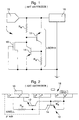
- Figures 1 and 2 of the present description respectively represent a diagram electric of such a circuit, and a sectional view transverse of a semiconductor substrate in which is formed this circuit.
- the circuit designated by the reference 1 includes an SCR 10 structure formed by a transistor bipolar type 12 PNP, and by a bipolar transistor type 14 NPN.
- Transistors 12 and 14 are coupled transversely between a connection pad 15 of a integrated circuit 16 to be protected, and the mass of this circuit. More specifically, the emitter terminal of transistor 12 is connected to pad 15, as well as the collector terminal of transistor 14 via a Rw resistor. and the emitter terminal of transistor 14 is connected to the earth of circuit 16, as well as the collector terminal of transistor 12 via a resistor Rs.
- the transistor 12 is formed in a box area having an N-type conductivity, this area being designated by the reference "NWELL”, and the transistor 14 is formed in a substrate having a P-type conductivity - , this substrate being designated by the reference "p-sub”.
- the resistances of the NWELL zone and of the substrate in which the SCR structure 10 as a whole is formed correspond respectively to the resistances Rw and Rs.
- Circuit 1 further includes an effect transistor field 18 to N channel to lower the voltage of triggering of the SCR 10 structure at a value equal to the avalanche voltage of transistor 18.
- a disadvantage of such a protection circuit 1 lies in the fact that, following a discharge electrostatic, transistor 18 may not trigger, which does not provide good immunity to electrical overvoltages induced by such discharges, as described in more detail in the US Patent already cited No. 5,400,202.
- FIGS. 1 and 2 Another disadvantage of a protective structure as described in relation to FIGS. 1 and 2, lies in the fact that it does not allow the application of electrical potentials greater than the potential of the circuit protected by this structure, nor the application of electrical potentials lower than the ground potential of this circuit.
- This structure includes a first bipolar transistor, which has its emitter connected to a external terminal of the integrated circuit and its collector connected to the mass.
- the structure also includes a second bipolar transistor, which has its emitter connected to the external terminal of the integrated circuit, and its connected collector at its base and at the base of the first transistor, a diode being inversely connected between the collector of the second transistor and ground.
- the structure also includes a field effect transistor including gate and drain are connected to the external terminal of the integrated circuit and the substrate and the source are connected to the collector of the second transistor.
- the first bipolar transistor is defined by a first diffusion zone of a first type of conductivity carried out in a box of a second type of conductivity, and the semiconductor substrate of a first conductivity type.
- the second bipolar transistor is defined by the first broadcast area and a second diffusion area in the box, which is connected to the caisson.
- the diode is defined by the box and the semiconductor substrate, while the effect transistor of field is defined by the two diffusion zones and a grid between the two diffusion zones.
- This structure has the disadvantage of being complicated and does not guarantee identical protection depending on positive or negative polarity of discharges electrostatic which can disturb the circuit to be protected.
- a transponder is a device comprising a means for processing data, a coil or antenna arranged to receive a radio signal containing data identification for example, and to provide in response this data in the form of an electrical signal supplied to the means of treatment, and vice versa.
- Current transponders can receive radio signals inducing on the coil electrical potentials that exceed the range of usual operation between potential supply provided by means of data processing and the ground potential of the transponder.
- An object of the present invention is to provide a discharge protection structure electrostatic can be connected to a terminal external of a circuit to be protected, this overcoming structure the difficulties and disadvantages mentioned above.
- Another object of the present invention is to provide such a protective structure allowing the application to said external terminal of potentials electrical power greater than the supply potential of said circuit, as well as lower electrical potentials to the ground potential of the circuit.
- Another object of the present invention is to provide such a protective structure that meets the common concerns in the semiconductor industry, rationalization, size and cost.
- Another object of the present invention is to provide an assembly including a protective structure connected to an external terminal of a circuit to be protected so to overcome the aforementioned drawbacks.
- the protective structure according to this invention can be connected to any circuit whose an external terminal is likely to be the seat of disturbances causing an abnormal elevation of the electrical potential present on this terminal with respect to the mass of said circuit.
- the reference A denotes said external terminal
- the reference Vdd denotes the supply potential supplied to said circuit
- the reference Vss designates the ground potential of this circuit.
- FIG 3 shows a cross-sectional view of a protective structure 20 according to the present invention, formed in a silicon substrate 30.
- the substrate 30 has a P-type conductivity -.
- a box area 32 is formed which has an N - type conductivity. Then three diffusion zones 34 to 36 having a P + type conductivity are formed in the box zone 32, as well as two diffusion zones 37 and 38 having a P + type conductivity in the substrate 30.
- Zones 34 to 38 are connected in the way next. Zones 34 and 37 are connected together, as well as the mass of the means 16, to receive the potential Vss. Likewise, zones 36 and 38 are connected between them, as well as to the mass of plea 16. And the area 35 is connected to the external terminal A.
- the protective structure 20 can be carried out according to a manufacturing chain of integrated circuit, the steps of which are known per se. So, the manufacturing process of the structure 20 is considered obvious to those skilled in the art, having regard to its knowledge in the field of manufacturing semiconductor products. And such a process whose directly obtained product is the type structure shown in Figure 3, will not be described in a way detailed in the present description.
- box area 32 is not connected to any electrical potential, since the N - P + junctions do not form ohmic contact between the areas 34 to 36 and the area 32. In other words , the box area 32 is arranged as a floating well.
- Figures 4A and 4B show two diagrams equivalent electrical protection structure 20, depending on the polarity of the electrical potential applied to the external terminal A.
- the reference VA indicates the potential applied to the external terminal A
- the reference IA designates the intensity of the electric current present at this terminal.
- Figure 5 shows a curve 50 illustrating the relationship between the electrical potential VA and IA intensity.
- the potential of the box area 32 is substantially equal to the potential VA, as long as the potential VA is less than a threshold + Vbd.
- the N + P junction - between the box area 32 and the area 34 is reverse biased, as well as the N + P junction - between the box area 32 and the area 36. Consequently, as shown in FIG. 5 , the intensity IA is zero, when the potential VA is between the potential Vss and the threshold + Vbd.
- the threshold + Vbd represents the breakdown threshold of the junctions P + N - between the zones 34 to 36 and the box zone 32.
- the voltage threshold Vbd may be of the order of 16 V , for processes for manufacturing usual semiconductor products.
- the junction P + N - between zone 35 and well zone 32 thus polarized corresponds to a direct polarized diode.
- the junction P + N - between the zone 34 and the well-polarized box zone 32 corresponds to a reverse biased diode.
- the P + N-junction between the zone 36 and the well-polarized box zone 32 corresponds to a reverse biased diode.
- the well zone 32 is no longer a floating well, and the potential of zones 34 and 36 is fixed at the threshold + Vbd.
- Zone 35 constitutes the emitters of transistors 41 and 42, and zones 34 and 36 respectively constitute the collectors of these two transistors. And the regions 32a and 32b respectively constitute the bases of the transistors 41 and 42. These are connected between them by an electrical resistance 44 which corresponds to resistive path in the box area 32 between the regions 32a and 32b.
- the intensity IA is zero, when the potential VA is between the potential Vss and a threshold -Vbd which is equal to the opposite of the threshold + Vbd.
- the protective structure 20 is electrically equivalent to bipolar transistors 41 and 42 connected as shown in FIG. 4B and described below.
- Zone 35 constitutes the collectors of the transistors 41 and 42, and zones 34 and 36 respectively constitute the emitters of these two transistors, regions 32a and 32b respectively constituting the bases of the transistors 41 and 42.
- the characteristic between the potential VA and the intensity IA of the external terminal A of the circuit protected by structure 20 performs two particularly advantageous functions compared to conventional protective structures of the aforementioned type.
- the functioning of the structure of protection according to the present invention allows the implementation work of this structure in the case of an application to a circuit to operate at electrical potentials greater than the supply potential (which is typically around +5 V), or less than circuit ground potential.
Landscapes
- Semiconductor Integrated Circuits (AREA)
- Emergency Protection Circuit Devices (AREA)
- Liquid Crystal (AREA)
- Radar Systems Or Details Thereof (AREA)
- Transmitters (AREA)
- Bipolar Integrated Circuits (AREA)
Claims (3)
- Schutzstruktur (20), die an einen externen Anschluss (A) einer vor elektrostatischen Entladungen zu schützenden Schaltung (16) angeschlossen werden kann, wobei diese Struktur durch drei Diffusionszonen (34, 35, 36) gebildet ist, die von einem ersten Leitfähigkeitstyp sind und in einer schwebenden Wannenzone (32) ausgebildet sind, die von einem zweiten Leitfähigkeitstyp ist, wobei die schwebende Wannenzone in einem Halbleitersubstrat (30) ausgebildet ist, das von dem ersten Leitfähigkeitstyp ist, dadurch gekennzeichnet, dass zwei (34, 36) der drei Zonen mit einem elektrischen Referenzpotential (Vss) verbunden sind und dass die andere Zone (35) an den externen Anschluss angeschlossen sein kann, wobei die drei Zonen so beschaffen sind, dass sie Bipolartransistoren (41, 42) definieren, deren Basis sich in der schwebenden Wannenzone befindet.
- Baueinheit, die eine Schutzstruktur (20) nach Anspruch 1 sowie eine durch die Struktur zu schützende integrierte Schaltung umfasst, dadurch gekennzeichnet, dass die integrierte Schaltung (16) ein an eine Sende/Empfangs-Antenne angeschlossener Transponder ist und dass der externe Anschluss (A) an einen der Anschlüsse dieser Antenne angeschlossen ist, so dass der Transponder durch die Schutzstruktur geschützt ist.
- Baueinheit nach Anspruch 2, dadurch gekennzeichnet, dass die Struktur (20) und die integrierte Schaltung (16) monolithisch im selben Halbleitersubstrat (30) ausgebildet sind.
Priority Applications (3)
| Application Number | Priority Date | Filing Date | Title |
|---|---|---|---|
| EP98104915A EP0944151B1 (de) | 1998-03-18 | 1998-03-18 | Schutzstruktur einer Schaltung gegen elektrostatische Entladung |
| AT98104915T ATE255782T1 (de) | 1998-03-18 | 1998-03-18 | Schutzstruktur einer schaltung gegen elektrostatische entladung |
| DE1998620225 DE69820225T2 (de) | 1998-03-18 | 1998-03-18 | Schutzstruktur einer Schaltung gegen elektrostatische Entladung |
Applications Claiming Priority (1)
| Application Number | Priority Date | Filing Date | Title |
|---|---|---|---|
| EP98104915A EP0944151B1 (de) | 1998-03-18 | 1998-03-18 | Schutzstruktur einer Schaltung gegen elektrostatische Entladung |
Publications (2)
| Publication Number | Publication Date |
|---|---|
| EP0944151A1 EP0944151A1 (de) | 1999-09-22 |
| EP0944151B1 true EP0944151B1 (de) | 2003-12-03 |
Family
ID=8231603
Family Applications (1)
| Application Number | Title | Priority Date | Filing Date |
|---|---|---|---|
| EP98104915A Expired - Lifetime EP0944151B1 (de) | 1998-03-18 | 1998-03-18 | Schutzstruktur einer Schaltung gegen elektrostatische Entladung |
Country Status (3)
| Country | Link |
|---|---|
| EP (1) | EP0944151B1 (de) |
| AT (1) | ATE255782T1 (de) |
| DE (1) | DE69820225T2 (de) |
Family Cites Families (4)
| Publication number | Priority date | Publication date | Assignee | Title |
|---|---|---|---|---|
| US4829350A (en) * | 1988-05-05 | 1989-05-09 | National Semiconductor Corporation | Electrostatic discharge integrated circuit protection |
| IT1253683B (it) * | 1991-09-12 | 1995-08-22 | Sgs Thomson Microelectronics | Dispositivo a bassa corrente di perdita per la protezione di un circuito integrato da scariche elettrostatiche. |
| US5291051A (en) * | 1992-09-11 | 1994-03-01 | National Semiconductor Corporation | ESD protection for inputs requiring operation beyond supply voltages |
| JP3461197B2 (ja) * | 1994-05-02 | 2003-10-27 | パイオニア株式会社 | 静電破壊防止回路 |
-
1998
- 1998-03-18 AT AT98104915T patent/ATE255782T1/de not_active IP Right Cessation
- 1998-03-18 DE DE1998620225 patent/DE69820225T2/de not_active Expired - Lifetime
- 1998-03-18 EP EP98104915A patent/EP0944151B1/de not_active Expired - Lifetime
Also Published As
| Publication number | Publication date |
|---|---|
| EP0944151A1 (de) | 1999-09-22 |
| DE69820225D1 (de) | 2004-01-15 |
| DE69820225T2 (de) | 2004-11-18 |
| ATE255782T1 (de) | 2003-12-15 |
Similar Documents
| Publication | Publication Date | Title |
|---|---|---|
| FR2812972A1 (fr) | Dispositif a semiconducteur consistant en un thyristor pour la protection contre les decharges electrostatiques | |
| US10930640B2 (en) | Intelligent diode structures | |
| EP0543742A1 (de) | Monolithische Niederspannungsschutzdiode mit geringer Kapazität | |
| EP2290691A1 (de) | Schutzvorrichtung für einen integrierten Schaltkreis gegen elektrostatische Entladungen | |
| FR3016999A1 (fr) | Dispositif electronique, en particulier pour la protection contre les decharges electrostatiques | |
| EP0543745B1 (de) | MOS-Transistor mit integrierter Zener-Schutzdiode | |
| FR2748854A1 (fr) | Structure de protection contre une decharge electrostatique pour circuit integre cmos | |
| KR20090091711A (ko) | 정전기 방전 이벤트로부터 반도체 디바이스를 보호하는 정전기 방전 보호 디바이스 및 방법 | |
| EP0780952A1 (de) | Monolithischer und statischer Strombegrenzer und Schutzschalter | |
| FR2763175A1 (fr) | Dispositif semiconducteur de puissance | |
| EP0944151B1 (de) | Schutzstruktur einer Schaltung gegen elektrostatische Entladung | |
| FR2770341A1 (fr) | Dispositif de protection contre des decharges electrostatiques a faible niveau de seuil | |
| FR3131981A1 (fr) | Dispositif de protection contre les décharges électrostatiques | |
| FR3095891A1 (fr) | Circuit électronique | |
| FR2719158A1 (fr) | Circuit d'entrée pour protéger un circuit intégré monolithe. | |
| US7382039B2 (en) | Edge seal for improving integrated circuit noise isolation | |
| EP0697734B1 (de) | Schutzschaltung gegen elektrostatische Entladung | |
| FR3044166A1 (fr) | Dispositif electronique, en particulier pour la protection contre des surtensions | |
| FR2875335A1 (fr) | Circuit electronique a double alimentation et a moyens de protection contre les claquages, et moyens de protection correspondants | |
| EP0881681B1 (de) | Anordnung zum Schützen einer integrierten MOS-Vorrichtung gegen Spannungsabfälle | |
| FR3092699A1 (fr) | Dispositif semiconducteur de thyristor et procédé de fabrication correspondant | |
| US6534834B1 (en) | Polysilicon bounded snapback device | |
| FR2764735A1 (fr) | Protection du caisson logique d'un composant incluant un transistor mos de puissance integre | |
| EP0820135A1 (de) | Statischer selbsthaltender Mikroschalter | |
| US7622792B2 (en) | Semiconductor device and method of manufacturing the same |
Legal Events
| Date | Code | Title | Description |
|---|---|---|---|
| PUAI | Public reference made under article 153(3) epc to a published international application that has entered the european phase |
Free format text: ORIGINAL CODE: 0009012 |
|
| AK | Designated contracting states |
Kind code of ref document: A1 Designated state(s): AT BE CH DE FR GB IE IT LI |
|
| AX | Request for extension of the european patent |
Free format text: AL;LT;LV;MK;RO;SI |
|
| 17P | Request for examination filed |
Effective date: 20000322 |
|
| AKX | Designation fees paid |
Free format text: AT BE CH DE FR GB IE IT LI |
|
| 17Q | First examination report despatched |
Effective date: 20021025 |
|
| GRAH | Despatch of communication of intention to grant a patent |
Free format text: ORIGINAL CODE: EPIDOS IGRA |
|
| RIC1 | Information provided on ipc code assigned before grant |
Ipc: 7H 01L 27/02 B Ipc: 7H 02H 9/04 A |
|
| GRAS | Grant fee paid |
Free format text: ORIGINAL CODE: EPIDOSNIGR3 |
|
| GRAA | (expected) grant |
Free format text: ORIGINAL CODE: 0009210 |
|
| RBV | Designated contracting states (corrected) |
Designated state(s): AT BE CH DE FR GB IE IT LI NL |
|
| AK | Designated contracting states |
Kind code of ref document: B1 Designated state(s): AT BE CH DE FR GB IE IT LI NL |
|
| PG25 | Lapsed in a contracting state [announced via postgrant information from national office to epo] |
Ref country code: NL Free format text: LAPSE BECAUSE OF FAILURE TO SUBMIT A TRANSLATION OF THE DESCRIPTION OR TO PAY THE FEE WITHIN THE PRESCRIBED TIME-LIMIT Effective date: 20031203 Ref country code: IT Free format text: LAPSE BECAUSE OF FAILURE TO SUBMIT A TRANSLATION OF THE DESCRIPTION OR TO PAY THE FEE WITHIN THE PRESCRIBED TIME-LIMIT;WARNING: LAPSES OF ITALIAN PATENTS WITH EFFECTIVE DATE BEFORE 2007 MAY HAVE OCCURRED AT ANY TIME BEFORE 2007. THE CORRECT EFFECTIVE DATE MAY BE DIFFERENT FROM THE ONE RECORDED. Effective date: 20031203 Ref country code: IE Free format text: LAPSE BECAUSE OF FAILURE TO SUBMIT A TRANSLATION OF THE DESCRIPTION OR TO PAY THE FEE WITHIN THE PRESCRIBED TIME-LIMIT Effective date: 20031203 Ref country code: AT Free format text: LAPSE BECAUSE OF FAILURE TO SUBMIT A TRANSLATION OF THE DESCRIPTION OR TO PAY THE FEE WITHIN THE PRESCRIBED TIME-LIMIT Effective date: 20031203 |
|
| REG | Reference to a national code |
Ref country code: GB Ref legal event code: FG4D Free format text: NOT ENGLISH |
|
| REG | Reference to a national code |
Ref country code: CH Ref legal event code: EP |
|
| REG | Reference to a national code |
Ref country code: IE Ref legal event code: FG4D Free format text: FRENCH |
|
| REF | Corresponds to: |
Ref document number: 69820225 Country of ref document: DE Date of ref document: 20040115 Kind code of ref document: P |
|
| PG25 | Lapsed in a contracting state [announced via postgrant information from national office to epo] |
Ref country code: BE Free format text: LAPSE BECAUSE OF NON-PAYMENT OF DUE FEES Effective date: 20040331 |
|
| REG | Reference to a national code |
Ref country code: CH Ref legal event code: NV Representative=s name: ICB INGENIEURS CONSEILS EN BREVETS SA |
|
| GBT | Gb: translation of ep patent filed (gb section 77(6)(a)/1977) |
Effective date: 20040322 |
|
| NLV1 | Nl: lapsed or annulled due to failure to fulfill the requirements of art. 29p and 29m of the patents act | ||
| RIC2 | Information provided on ipc code assigned after grant |
Ipc: 7H 02H 9/04 A |
|
| REG | Reference to a national code |
Ref country code: IE Ref legal event code: FD4D |
|
| BERE | Be: lapsed |
Owner name: S.A. *EM MICROELECTRONIC-MARIN Effective date: 20040331 |
|
| PLBE | No opposition filed within time limit |
Free format text: ORIGINAL CODE: 0009261 |
|
| STAA | Information on the status of an ep patent application or granted ep patent |
Free format text: STATUS: NO OPPOSITION FILED WITHIN TIME LIMIT |
|
| 26N | No opposition filed |
Effective date: 20040906 |
|
| PGFP | Annual fee paid to national office [announced via postgrant information from national office to epo] |
Ref country code: GB Payment date: 20110224 Year of fee payment: 14 |
|
| GBPC | Gb: european patent ceased through non-payment of renewal fee |
Effective date: 20120318 |
|
| PG25 | Lapsed in a contracting state [announced via postgrant information from national office to epo] |
Ref country code: GB Free format text: LAPSE BECAUSE OF NON-PAYMENT OF DUE FEES Effective date: 20120318 |
|
| REG | Reference to a national code |
Ref country code: FR Ref legal event code: PLFP Year of fee payment: 19 |
|
| REG | Reference to a national code |
Ref country code: FR Ref legal event code: PLFP Year of fee payment: 20 |
|
| PGFP | Annual fee paid to national office [announced via postgrant information from national office to epo] |
Ref country code: DE Payment date: 20170222 Year of fee payment: 20 Ref country code: CH Payment date: 20170227 Year of fee payment: 20 Ref country code: FR Payment date: 20170221 Year of fee payment: 20 |
|
| REG | Reference to a national code |
Ref country code: DE Ref legal event code: R071 Ref document number: 69820225 Country of ref document: DE |
|
| REG | Reference to a national code |
Ref country code: CH Ref legal event code: PL |