EP0944299A2 - Abschirmungsmaterial gegen elektrische Wellen - Google Patents
Abschirmungsmaterial gegen elektrische Wellen Download PDFInfo
- Publication number
- EP0944299A2 EP0944299A2 EP99302158A EP99302158A EP0944299A2 EP 0944299 A2 EP0944299 A2 EP 0944299A2 EP 99302158 A EP99302158 A EP 99302158A EP 99302158 A EP99302158 A EP 99302158A EP 0944299 A2 EP0944299 A2 EP 0944299A2
- Authority
- EP
- European Patent Office
- Prior art keywords
- electric wave
- electrically conductive
- light transmitting
- conductive layer
- wave shielding
- Prior art date
- Legal status (The legal status is an assumption and is not a legal conclusion. Google has not performed a legal analysis and makes no representation as to the accuracy of the status listed.)
- Withdrawn
Links
Images

Classifications
-
- H—ELECTRICITY
- H05—ELECTRIC TECHNIQUES NOT OTHERWISE PROVIDED FOR
- H05K—PRINTED CIRCUITS; CASINGS OR CONSTRUCTIONAL DETAILS OF ELECTRIC APPARATUS; MANUFACTURE OF ASSEMBLAGES OF ELECTRICAL COMPONENTS
- H05K9/00—Screening of apparatus or components against electric or magnetic fields
- H05K9/0001—Rooms or chambers
- H05K9/0005—Shielded windows
-
- B—PERFORMING OPERATIONS; TRANSPORTING
- B32—LAYERED PRODUCTS
- B32B—LAYERED PRODUCTS, i.e. PRODUCTS BUILT-UP OF STRATA OF FLAT OR NON-FLAT, e.g. CELLULAR OR HONEYCOMB, FORM
- B32B27/00—Layered products comprising a layer of synthetic resin
- B32B27/06—Layered products comprising a layer of synthetic resin as the main or only constituent of a layer, which is next to another layer of the same or of a different material
-
- H—ELECTRICITY
- H05—ELECTRIC TECHNIQUES NOT OTHERWISE PROVIDED FOR
- H05K—PRINTED CIRCUITS; CASINGS OR CONSTRUCTIONAL DETAILS OF ELECTRIC APPARATUS; MANUFACTURE OF ASSEMBLAGES OF ELECTRICAL COMPONENTS
- H05K9/00—Screening of apparatus or components against electric or magnetic fields
- H05K9/0073—Shielding materials
- H05K9/0094—Shielding materials being light-transmitting, e.g. transparent, translucent
Definitions
- This invention relates to an electric wave shielding material to be stuck to a window or other surface (termed an "adherend” herein) of construction or a moving vehicle, such as an automobile, a train, and an airplane, to shield an electric wave.
- electric wave shielding materials for use in the window of the construction and the wall in room of hospital, various types have been suggested.
- One example includes an electric wave shielding material for wall disclosed in Japanese Utility Model Laid-Open No. 59-78696 in which a metal foil is laminated on the top surface of a backing material via an adhesive, and a flexible synthetic resin is further laminated on the top surface of the metal foil via an adhesive.
- an electric wave shielding material in which a room to be applied is perfectly covered with an electrically conductive material such as a metal foil made, e.g., of copper or aluminum, or carbon fiber during the course of construction to thereby carry out the electric shielding.
- an electrically conductive material such as a metal foil made, e.g., of copper or aluminum, or carbon fiber during the course of construction to thereby carry out the electric shielding.
- a known electric wave shielding material for an application to a window is an electric wave shielding paint which is light transmitting.
- the electric wave shielding paint shields an electric wave by applying it to a site required for shielding an electric wave such as a window.
- Such a type of the electric shielding paint is disadvantageous in that skill is required to uniformly apply the electric shielding paint, and the application thereof is worse in the working efficiency.
- a general aim of the present invention is, therefore, to provide an electric wave shielding material which can be stuck with ease, which ensures the shielding of electric wave, and which can be stuck to a site such as a window glass at which a transparency is required.
- a preferred object of the present invention is to provide an electric wave shielding material, which can selectively shield an electric wave having a specific wavelength region.
- an electric wave shielding material to be utilized with being stuck to an adherend which comprises:
- an electric wave shielding material to be utilized with being stuck to an adherend which comprises: a light transmitting surface material, a light transmitting electrically conductive layer provided on one surface of the surface material, a member for converting an electric wave into a heat energy connected to said light transmitting electrically conductive layer and a light transmitting adhesive layer provided on at least part of said surface material, said light transmitting electrically conductive layer or said member for converting an electric wave into a heat energy.
- the third aspect of the present invention concerns an electric wave shielding material to be utilized with being stuck to an adherend, which comprises: a light transmitting surface material, at least one electrically conductive layer, which resonates at a prescribed wavelength region, provided on one surface of the surface material, and a member for converting an electric wave into a heat energy provided in such a manner that it is connected to the electrically conductive layer, which also comprises an adhesive layer provided on one or the other surface of the surface material.
- the electric wave shielding material 11 of the first embodiment of the present invention is composed of a body member 17 and a connecting piece 19 which is formed separately from the body member 17.
- the body member 17 comprises a light transmitting surface material 12, a light transmitting electrically conductive layer 13 provided on one surface of the surface material 12, a light transmitting adhesive layer 14 provided on at least a part of the light transmitting electrically conductive layer 13 in such a manner that a part of the light transmitting electrically conductive layer 13 is exposed to form a connecting electrically conductive portion 16, and a release liner 15.
- the connecting piece 19 possesses a member for converting an electric wave into a heat energy.
- the surface material 12 is provided for the purpose of protecting the surface of the electric wave shielding material according to the present invention, and preventing the inter layers from being exposed, and is required to have light transmitting property.
- the surface material 12 which can be used in the present invention is not restricted as long as it meets the above conditions. Examples include, but are not restricted to, films produced from polyethylene terephthalate, polyethylene, polypropylene, polystyrene, polyvinyl chloride, and polyethylene naphthate. Preference is given to use a film from polyethylene terephthalate or polyolefin, in terms of the fact that no harmful substance is generated even if it is burned off and it can easily be obtained.
- the thickness of the film is not restricted as long as the objects and the effects of the presented invention can be obtained.
- the thickness is freely selected considering the applicability of the film, light transmitting property, the total thickness of the electric wave shielding material of the present invention, and any other factors, and generally in the range of from 10 to 1,000 ⁇ m, preferably 25 to 200 ⁇ m, and particularly approximately 50 ⁇ m.
- the light transmitting electrically conductive layer 13 is a layer for the purpose of shielding an electric wave to be shielded, and is composed, e.g., of indium tin oxide (hereinafter abbreviated as "ITO"), metals such as aluminum, gold, silver, copper, nickel, iron, and tin, and metal oxides thereof, and organic electrically conductive agents such as polypyrrole, polyaniline, and polyacetylene.
- ITO indium tin oxide
- metals such as aluminum, gold, silver, copper, nickel, iron, and tin
- organic electrically conductive agents such as polypyrrole, polyaniline, and polyacetylene.
- the thickness of the light transmitting electrically conductive layer depends on the metal or the oxide thereof used, and generally speaking it is preferably in the range of from 0.1 to 10 ⁇ m. If the thickness is less than 0.1 ⁇ m, the electric wave shielding properties is undesirably reduced. Conversely, if it exceeds 10 ⁇ m, the light transmitting property is undesirably reduced, particularly in the case where the electric wave shielding material is to be stuck to a window portion required for securing visibility.
- the formation of the light transmitting electrically conductive layer 13 is not restricted as long as the electrically conductive layer can be suitably formed, such as deposition, sputtering, plating, printing.
- the light transmitting adhesive layer 14 is provided on the laminate composed of the surface material 12 and the light transmitting electrically conductive layer 13.
- the light transmitting adhesive layer 14 is provided for the purpose of sticking the electric wave shielding material according to the present invention onto the adherend such as a window, and is required to have a light transmitting property.
- the adhesive for forming such a light transmitting adhesive layer 14 is not specially restricted as long as it possesses a light transmitting property, and examples include acrylic adhesives, epoxy adhesives, rubber adhesives, silicone adhesives, polyurethane adhesives, polyethylene heat sealing adhesives, and the like.
- the light transmitting adhesive layer 14 may be provided on the whole of the rear surface of the light transmitting electrically conductive layer 13, or may be provided on the rear surface at several intervals.
- the thickness of the adhesive layer is also not specifically restricted as long as it is a thickness for securely sticking the electric wave shielding material according to the present invention on the adherend, and for example it is in the range of from 5 to 50 ⁇ m.
- a connecting electrically conductive portion 16 is formed at one end of the light transmitting electrically conductive layer 13 in such a manner that a part of light transmitting electrically conductive layer 13 is exposed.
- the connecting electrically conductive portion 16 is a region formed for the purpose of directly connecting the light transmitting electrically conductive layer 13 to the connecting piece 19, which will be described below.
- the width of the connecting electrically conductive portion 16 is freely selected depending upon the connecting piece, and generally is approximately 2 cm.
- the electric wave shielding material according to the first aspect of the present invention is composed of the body member 17 and the connecting piece 19.
- the connecting piece 19 is composed of a member for converting an electric wave into a heat energy, and is provided for the purpose of converting the electric wave absorbed on the body member 17 into a heat energy.
- the connecting piece 19 is composed mainly of a center layer 19b based on a plastic film such as polyurethane, polyvinyl chloride, or polystyrene, or non-woven fabric into which a member for converting an electric wave into a heat energy such as carbon powder or ferrite is incorporated.
- a layer 19a comprising an electrically conductive adhesive
- a layer 19c comprising acrylic adhesive
- a release liner is provided on each of the electrically conductive adhesive layer. When used, the release liners are peeled to stick the connecting piece to the window and to the connecting electrically conductive portion 16.
- the connecting piece is formed into the width substantially the same as that of the connecting electrically conductive portion 16.
- the content of the member for converting an electric wave into a heat energy such as carbon powder or ferrite is from 10 to 1,000 parts by weight, based on 100 parts by weight of the base plastic film or base nonwoven fabric.
- the electrically conductive adhesive 19a and the acrylic adhesive 19c are previously laminated with release liners, respectively, and each of the release liners is removed when used, making it possible to easily operate these adhesives.
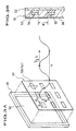
- the connecting piece 19 is stuck such a manner that the connecting piece 19 is brought into contact with the frame 20a of the window 20, then the release liner 18 is removed from the connecting piece 19. Subsequently, the release liner 15 is removed from the body member 17, and the body member 17 is stuck onto the window 20 via the adhesive layer 14 in such a manner that the surface of the connecting electrically conductive portion 16 is superposed on the electrically conductive adhesive 19a of the connecting piece 19.
- the electric wave shielding material 11 As described above, it becomes easy to stick the electric wave shielding material 11 in a suitable state.
- the electric wave such as from a portable phone, which will be penetrated through the window is transmitted to the polyurethane film 19b via the electrically conductive layer 13 of the electric wave shielding material 11, and the electric wave is then converted into heat energy by means of carbon powder contained in the polyurethane film 19b.
- the electric wave shielding material 21B is composed of a light transmitting surface material 22B, a light transmitting electrically conductive layer 23B provided on one surface of the surface material 22B, a member 28b for converting an electric wave into a heat energy provided on one end of the light transmitting electrically conductive layer 23B via electrically conductive adhesives 28a, a light transmitting adhesive layer 24B provided on one surface of the light transmitting electrically conductive layer 23B, and an adhesive layer 28C provided on the member 28b for converting an electric wave into a heat energy.
- a difference between the electric wave shielding materials according to the first embodiment and the second embodiment of the present invention is that whereas the connecting piece containing the member for converting an electric wave into a heat energy is separately provided in the first aspect of the present invention, they are provided together by connecting them in the second aspect of the present invention. Therefore, the surface material 22B, the light transmitting adhesive layer 24B, the light transmitting electrically conductive layer 23B and the method of the construction of them are similar to those of the first embodiment of the present invention. So, repeated description is unnecessary.
- the sticking is carried out according to the following procedure: The whole of the electric wave shielding material 21B is stuck on the window in such a manner that circumference of the electric wave shielding material 21B is along with the frame 91 to cover the whole surface of the window with the electric wave shielding material 21B.
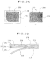
- the electric wave shielding material 51 according to the third embodiment of the present invention is stuck to a window 90. It is composed of a plurality of electrically conductive layers 53, which resonate at a prescribed electric wavelength region to be shielded.
- the electrically conductive layers 53 are arranged on the surface material 52 so that the distance d between the electrically conductive layers 53 is less than half of the wavelength ⁇ to be shielded.
- the size, L, of the electrically conductive layer 53 in the width direction is formed so as to be half of the wavelength ⁇ to be shielded.
- a polyurethane film 54 into which carbon powder which is a member for converting an electric wave into a heat energy is incorporated is provided on the rear surface of the electrically conductive layer 53. Moreover, on the rear surface of the polyurethane film 54 is provided an adhesive layer 55. On the adhesive side of the adhesive layer is provided a release liner 56.
- the surface material 52 which can be used is the same as the surface material 12 described above. Also, the electrically conductive layer 53 maybe the same as the electrically conductive layer 13, and the adhesive layer 55 maybe the same as the adhesive layer 14.
- the electric wave having a desired wavelength such can be shielded.
- two or more electric waves each having different wavelength are desired to be shielded, when several electrically conductive layers each corresponding to desired electric wavelength are provided, these electric waves can be shielded.
- the electric wavelength shielding materials illustrated by the first to the third embodiments of the present invention can be stuck to window portions of automobiles, trains such as super express, airplane, etc.
- the adhesive layer is not necessarily provided over the whole surface of the electric wave shielding material, and the adhesive layer is partially provided in such an extent that the electric wave shielding material is stuck to and fixed to the surface of the object
- a polyethylene terephthalate (PET) film having a thickness of 50 ⁇ m was used as a surface material.
- an ITO layer as an electrically conductive layer, having a thickness of 0.2 ⁇ m to provide an assembly.
- the assembly was cut into a size of 500 mm in length and 500 mm in width, and then an acrylic adhesive comprising polybutylacrylate as main ingredient was applied to the ITO layer so as to leave a margin having a size of 500 mm in length and 10 mm in width from the end portion to thereby form an acrylic adhesive layer having a thickness of 25 ⁇ m.
- Onto the adhesive layer thus formed was applied a 38 ⁇ m thick PET film having a size of 500 mm in length and 500 mm in width to which a releasing treatment with a silicone resin had been applied to produce a body of the electric wave shielding material.
- an electrically conductive adhesive comprising 30% by weight of an acrylic adhesive comprising polybutylacrylate as main ingredient having 70% by weight of nickel powder uniformly dispersed therewith was applied so as to form an electrically conductive adhesive layer having a thickness after drying of 25 ⁇ m.
- a polyurethane resin solution was prepared by mixing 145 parts by weight of a 65% Takelac A-540 solution with a 18 parts by weight of 70% Takenate solution A-12 (both available from TAKEDA CHEMICAL INDUSTRIES LTD.) and stirring the mixture.
- the polyurethane solution in an amount of 60 parts by weight was mixed and stirred with 40 parts by weight of carbon powder.
- the mixture was applied onto the electrically conductive layer so as to form a member for converting an electric wave to a heat energy having a dry thickness of 40 ⁇ m (dried at 100°C for 30 minutes).
- the connecting piece was produced by applying an electrically conductive adhesive composed of 30% by weight of an adhesive comprising polybutylacrylate as main ingredient and 70% by weight of nickel powder onto the member for converting an electric wave to a heat energy formed as described above so as to form an electrically adhesive layer having a thickness of 25 ⁇ m after drying.
- the connecting piece produced as described above was stuck such a manner that the connecting piece was in contact with the frame, as the release liner was gradually peeled off. Further, the release liner of the body of the electric wave shielding material was peeled off, and the body was stuck to the window glass via an adhesive layer provided on the surface material so as to overlap the rear surface of the electrically conductive layer with the electrically conductive adhesive portion of the connecting piece.
- An electric wave shielding material was produced by peeling the release liner of the body of the electric wave shielding material and laminating it with the connecting piece such a manner that the rear surface of the connecting electrically conductive portion was overlapped with the electrically conductive adhesive layer of the connecting piece. After the release liner of the connecting piece portion had been peeled off, the adhesive layer of the electric wave shielding material was stuck to the same window glass as described in Example 1 in such a manner that the connecting piece portion was in contact with the frame of the window.
- a transmitting antenna was set up on an outside of each of the windows and a receiving antenna was set up on an inside of the each of the windows, while setting the distance between a transmitting antenna and a receiving antenna at 1 m.
- electric waves each having a frequency as shown in Table 1 were transmitted to each of the windows, and the decreases in electric waves at the receiving antenna were examined by the use of a NETWORK-ANALYZER-MS4662A (produced by ANRITSU Corporation). The results are shown in Table 1. Decreases in Electric Waves Exemlified Window 1 Exemplified Window 2 Comparative Window 10 MHz 35 db 35 db None 100 MHz 29 db 29 db None 1,000 MHz 26 db 26 db None
- An electric wave shielding material capable of selectively shielding an electric wave was produced as follows: A polyurethane film (thickness: 500 ⁇ m) comprising the polyurethane resin and carbon powder having the same proportion as in the column of the connecting piece was thermally fused onto an aluminum foil (thickness: 10 ⁇ m), which was then cut into small pieces each having a size of 50 mm in length and 1 mm in width to form a member for converting an electric wave into a heat energy, provided on the electrically conductive layer. These pieces were stuck to a PET film (thickness: 50 ⁇ m) via an adhesive in such a manner the distance between pieces were 10 mm in both directions. Further, an acrylic adhesive was applied over the whole surface of the PET film to produce an electric wave shielding material of Example 3.
- Example 3 As in Examples 1 and 2, the electric shielding material of Example 3 was stuck to the same window glass as in the previous examples, the decrease in the electric wave was examined using the same device as in the previous examples. It was found that a decrease in an electric wave having a frequency of 3 GHz was 25 db.
- the present invention provides an electric wave shield for application to the surface of and adherend, preferably a light transmitting wall or window, the shield comprising:
Landscapes
- Engineering & Computer Science (AREA)
- Microelectronics & Electronic Packaging (AREA)
- Shielding Devices Or Components To Electric Or Magnetic Fields (AREA)
Applications Claiming Priority (2)
| Application Number | Priority Date | Filing Date | Title |
|---|---|---|---|
| JP6992998 | 1998-03-19 | ||
| JP06992998A JP4063945B2 (ja) | 1998-03-19 | 1998-03-19 | 電波シールド材 |
Publications (2)
| Publication Number | Publication Date |
|---|---|
| EP0944299A2 true EP0944299A2 (de) | 1999-09-22 |
| EP0944299A3 EP0944299A3 (de) | 2000-05-31 |
Family
ID=13416869
Family Applications (1)
| Application Number | Title | Priority Date | Filing Date |
|---|---|---|---|
| EP99302158A Withdrawn EP0944299A3 (de) | 1998-03-19 | 1999-03-19 | Abschirmungsmaterial gegen elektrische Wellen |
Country Status (3)
| Country | Link |
|---|---|
| US (1) | US6495752B1 (de) |
| EP (1) | EP0944299A3 (de) |
| JP (1) | JP4063945B2 (de) |
Cited By (9)
| Publication number | Priority date | Publication date | Assignee | Title |
|---|---|---|---|---|
| EP1196018A1 (de) * | 2000-10-05 | 2002-04-10 | Nisshinbo Industries, Inc. | Verfahren zur Ausbildung des Elektrodenbereiches auf der inneren Oberfläche eines elektromagnetische Wellen abschirmenden, lichtdurchlässigen Schirms und derart hergestellter Schirm |
| WO2002093995A1 (es) * | 2001-05-16 | 2002-11-21 | Advanced Shielding Technologies Europe S.L. | Compuesto protector de la radiación electromagnética en edificios formado por tres capas de resina |
| WO2004017700A1 (en) * | 2002-08-17 | 2004-02-26 | 3M Innovative Properties Company | Durable emi shielding film |
| US6929864B2 (en) | 2002-08-17 | 2005-08-16 | 3M Innovative Properties Company | Extensible, visible light-transmissive and infrared-reflective film and methods of making and using the film |
| US6933051B2 (en) | 2002-08-17 | 2005-08-23 | 3M Innovative Properties Company | Flexible electrically conductive film |
| US7215473B2 (en) | 2002-08-17 | 2007-05-08 | 3M Innovative Properties Company | Enhanced heat mirror films |
| WO2009058607A1 (en) * | 2007-10-30 | 2009-05-07 | 3M Innovative Properties Company | Multi-stack optical bandpass film with electro magnetic interference shielding for optical display filters |
| WO2011090450A1 (en) * | 2010-01-25 | 2011-07-28 | Uenal Fethi | Insulation of electromagnetic waves |
| US9822454B2 (en) | 2006-12-28 | 2017-11-21 | 3M Innovative Properties Company | Nucleation layer for thin film metal layer formation |
Families Citing this family (10)
| Publication number | Priority date | Publication date | Assignee | Title |
|---|---|---|---|---|
| EP1127381B1 (de) | 1998-11-02 | 2015-09-23 | 3M Innovative Properties Company | Transparente leitfähige oxide für kunststoff-flachbildschirme |
| JP2005108369A (ja) * | 2003-10-01 | 2005-04-21 | Hitachi-Lg Data Storage Inc | 光ディスク装置及びそれを搭載した携帯型情報処理装置 |
| US7495182B2 (en) * | 2004-01-30 | 2009-02-24 | Dai Nippon Printing Co., Ltd. | Electromagnetic wave shielding sheet and process for producing the same |
| US20060156318A1 (en) * | 2005-01-11 | 2006-07-13 | Hitachi - Lg Data Storage, Inc. | Optical disk apparatus and a portable information processing apparatus mounting the same therein |
| JP4969268B2 (ja) * | 2007-02-19 | 2012-07-04 | 三菱重工業株式会社 | 航空機用窓材およびその製造方法 |
| US8350451B2 (en) | 2008-06-05 | 2013-01-08 | 3M Innovative Properties Company | Ultrathin transparent EMI shielding film comprising a polymer basecoat and crosslinked polymer transparent dielectric layer |
| CN104968491A (zh) * | 2013-02-06 | 2015-10-07 | 旭硝子株式会社 | 透明面材以及使用该透明面材的显示装置 |
| US9497894B1 (en) * | 2015-07-22 | 2016-11-15 | John Gordon Ramsey | Low impedance radiofrequency shielded window |
| JP6184579B2 (ja) * | 2015-12-14 | 2017-08-23 | 日東電工株式会社 | 電磁波吸収体およびそれを備えた電磁波吸収体付成形体 |
| KR102514334B1 (ko) * | 2018-05-16 | 2023-03-27 | 쓰리엠 이노베이티브 프로퍼티즈 캄파니 | 차폐 테이프 |
Family Cites Families (5)
| Publication number | Priority date | Publication date | Assignee | Title |
|---|---|---|---|---|
| US4247737A (en) * | 1979-03-29 | 1981-01-27 | Spectrum Control, Inc. | Electromagnetically shielded viewing window |
| JPS5978696A (ja) * | 1982-10-28 | 1984-05-07 | Kanegafuchi Chem Ind Co Ltd | 光学活性オキサゾリジノン誘導体の製造方法 |
| CA2080177C (en) * | 1992-01-02 | 1997-02-25 | Edward Allan Highum | Electro-magnetic shield and method for making the same |
| JPH09321485A (ja) * | 1996-05-30 | 1997-12-12 | Achilles Corp | 電磁波遮蔽シート |
| JPH1013083A (ja) * | 1996-06-27 | 1998-01-16 | Tosoh Corp | 電磁波吸収体 |
-
1998
- 1998-03-19 JP JP06992998A patent/JP4063945B2/ja not_active Expired - Fee Related
-
1999
- 1999-03-19 EP EP99302158A patent/EP0944299A3/de not_active Withdrawn
- 1999-03-22 US US09/273,465 patent/US6495752B1/en not_active Expired - Fee Related
Cited By (16)
| Publication number | Priority date | Publication date | Assignee | Title |
|---|---|---|---|---|
| EP1196018A1 (de) * | 2000-10-05 | 2002-04-10 | Nisshinbo Industries, Inc. | Verfahren zur Ausbildung des Elektrodenbereiches auf der inneren Oberfläche eines elektromagnetische Wellen abschirmenden, lichtdurchlässigen Schirms und derart hergestellter Schirm |
| US6686536B2 (en) | 2000-10-05 | 2004-02-03 | Nisshinbo Industries, Inc. | Method of forming electrode section on inner surface of transparent electromagnetic wave shielding plate, and transparent electromagnetic wave shielding plate formed thereby |
| WO2002093995A1 (es) * | 2001-05-16 | 2002-11-21 | Advanced Shielding Technologies Europe S.L. | Compuesto protector de la radiación electromagnética en edificios formado por tres capas de resina |
| US7215473B2 (en) | 2002-08-17 | 2007-05-08 | 3M Innovative Properties Company | Enhanced heat mirror films |
| WO2004017699A1 (en) * | 2002-08-17 | 2004-02-26 | 3M Innovative Properties Company | Durable transparent emi shielding film |
| US6818291B2 (en) | 2002-08-17 | 2004-11-16 | 3M Innovative Properties Company | Durable transparent EMI shielding film |
| US6929864B2 (en) | 2002-08-17 | 2005-08-16 | 3M Innovative Properties Company | Extensible, visible light-transmissive and infrared-reflective film and methods of making and using the film |
| US6933051B2 (en) | 2002-08-17 | 2005-08-23 | 3M Innovative Properties Company | Flexible electrically conductive film |
| WO2004017700A1 (en) * | 2002-08-17 | 2004-02-26 | 3M Innovative Properties Company | Durable emi shielding film |
| US7261950B2 (en) | 2002-08-17 | 2007-08-28 | 3M Innovative Properties Company | Flexible, formable conductive films |
| US7351479B2 (en) | 2002-08-17 | 2008-04-01 | 3M Innovative Properties Company | Durable EMI shielding film |
| US7393557B2 (en) | 2002-08-17 | 2008-07-01 | 3M Innovative Properties | Flexible electrically conductive film |
| US9822454B2 (en) | 2006-12-28 | 2017-11-21 | 3M Innovative Properties Company | Nucleation layer for thin film metal layer formation |
| WO2009058607A1 (en) * | 2007-10-30 | 2009-05-07 | 3M Innovative Properties Company | Multi-stack optical bandpass film with electro magnetic interference shielding for optical display filters |
| US8630040B2 (en) | 2007-10-30 | 2014-01-14 | 3M Innovative Properties Company | Multi-component films for optical display filters |
| WO2011090450A1 (en) * | 2010-01-25 | 2011-07-28 | Uenal Fethi | Insulation of electromagnetic waves |
Also Published As
| Publication number | Publication date |
|---|---|
| US6495752B1 (en) | 2002-12-17 |
| JP4063945B2 (ja) | 2008-03-19 |
| EP0944299A3 (de) | 2000-05-31 |
| JPH11274791A (ja) | 1999-10-08 |
Similar Documents
| Publication | Publication Date | Title |
|---|---|---|
| EP0944299A2 (de) | Abschirmungsmaterial gegen elektrische Wellen | |
| US5401901A (en) | Weather-resistant electromagnetic interference shielding for electronic equipment enclosures | |
| CA2432970C (en) | Electromagnetic wave absorber | |
| EP2381756A2 (de) | Absorber für elektromagnetische Wellen | |
| EP1196018A1 (de) | Verfahren zur Ausbildung des Elektrodenbereiches auf der inneren Oberfläche eines elektromagnetische Wellen abschirmenden, lichtdurchlässigen Schirms und derart hergestellter Schirm | |
| EP1107355B1 (de) | Blattantenne mit resistiver Kohlenstoffschicht | |
| EP0930637A3 (de) | Abschirmung gegen die elektromagnetischen wellen, durchsichtige platte sowie Anzeige | |
| EP0754131B1 (de) | Schutzabdeckung | |
| EP0186517B1 (de) | Elektromagnetischer Rückstrahlungskörper | |
| US20010018123A1 (en) | Electromagnetic wave shielding device | |
| EP1758442B1 (de) | Elektromagnetische Wellen absorbierender Film und seine Herstellung | |
| JP3076473B2 (ja) | 積層型電波反射防止体及び電波反射防止方法 | |
| JP3209456B2 (ja) | 電波反射防止体および電波反射防止法 | |
| US4940619A (en) | Radiation absorption device | |
| US20020071551A1 (en) | Cellular phone electromagnetic wave earpiece shield | |
| GB2255313A (en) | Retro-reflective assembly | |
| CN2699590Y (zh) | 移动电话手机防辐射装置 | |
| JP3459630B2 (ja) | 電波吸収パネル | |
| GB1599063A (en) | Microwave oven window construction | |
| CN113601867A (zh) | 一种全波段雷达伪装网的加工工艺 | |
| JP3707263B2 (ja) | ディスプレイ用前面板 | |
| CN114736621A (zh) | 一种电磁屏蔽胶带及其制备方法 | |
| JPH037160B2 (de) | ||
| JP3802532B2 (ja) | 電波吸収体 | |
| JPH06224584A (ja) | 電波反射防止体及び電波反射防止方法 |
Legal Events
| Date | Code | Title | Description |
|---|---|---|---|
| PUAI | Public reference made under article 153(3) epc to a published international application that has entered the european phase |
Free format text: ORIGINAL CODE: 0009012 |
|
| AK | Designated contracting states |
Kind code of ref document: A2 Designated state(s): CH DE FR GB IT LI NL |
|
| AX | Request for extension of the european patent |
Free format text: AL;LT;LV;MK;RO;SI |
|
| RIN1 | Information on inventor provided before grant (corrected) |
Inventor name: SAKURAI, SATOSHI C/O LINTEC CORPORATION Inventor name: NAKATA, YASUKAZU C/O LINTEC CORPORATION Inventor name: SUGIZAKI, TOSHIO C/O LINTEC CORPORATION |
|
| PUAL | Search report despatched |
Free format text: ORIGINAL CODE: 0009013 |
|
| AK | Designated contracting states |
Kind code of ref document: A3 Designated state(s): AT BE CH CY DE DK ES FI FR GB GR IE IT LI LU MC NL PT SE |
|
| AX | Request for extension of the european patent |
Free format text: AL;LT;LV;MK;RO;SI |
|
| RIC1 | Information provided on ipc code assigned before grant |
Free format text: 7H 05K 9/00 A, 7B 60J 1/20 B |
|
| 17P | Request for examination filed |
Effective date: 20000623 |
|
| AKX | Designation fees paid |
Free format text: CH DE FR GB IT LI NL |
|
| STAA | Information on the status of an ep patent application or granted ep patent |
Free format text: STATUS: THE APPLICATION HAS BEEN WITHDRAWN |
|
| 18W | Application withdrawn |
Withdrawal date: 20020206 |