EP0944911B1 - Safety relay - Google Patents
Safety relay Download PDFInfo
- Publication number
- EP0944911B1 EP0944911B1 EP97948064A EP97948064A EP0944911B1 EP 0944911 B1 EP0944911 B1 EP 0944911B1 EP 97948064 A EP97948064 A EP 97948064A EP 97948064 A EP97948064 A EP 97948064A EP 0944911 B1 EP0944911 B1 EP 0944911B1
- Authority
- EP
- European Patent Office
- Prior art keywords
- capacitor
- state
- safety
- relay
- safety relay
- Prior art date
- Legal status (The legal status is an assumption and is not a legal conclusion. Google has not performed a legal analysis and makes no representation as to the accuracy of the status listed.)
- Expired - Lifetime
Links
- 239000003990 capacitor Substances 0.000 claims abstract description 72
- 239000004020 conductor Substances 0.000 claims abstract description 37
- 238000000034 method Methods 0.000 claims abstract description 19
- 230000008569 process Effects 0.000 claims abstract description 10
- 238000004519 manufacturing process Methods 0.000 claims abstract description 7
- 230000004044 response Effects 0.000 claims description 5
- 230000007704 transition Effects 0.000 claims 4
- 238000007599 discharging Methods 0.000 abstract description 3
- 238000010586 diagram Methods 0.000 description 9
- 239000004065 semiconductor Substances 0.000 description 7
- 230000008901 benefit Effects 0.000 description 4
- 230000007257 malfunction Effects 0.000 description 4
- 230000004913 activation Effects 0.000 description 3
- 208000027418 Wounds and injury Diseases 0.000 description 1
- 230000002159 abnormal effect Effects 0.000 description 1
- 230000003213 activating effect Effects 0.000 description 1
- 230000006378 damage Effects 0.000 description 1
- 230000005669 field effect Effects 0.000 description 1
- 208000014674 injury Diseases 0.000 description 1
- 238000012544 monitoring process Methods 0.000 description 1
- 230000010355 oscillation Effects 0.000 description 1
- 230000001960 triggered effect Effects 0.000 description 1
Images


Classifications
-
- H—ELECTRICITY
- H01—ELECTRIC ELEMENTS
- H01H—ELECTRIC SWITCHES; RELAYS; SELECTORS; EMERGENCY PROTECTIVE DEVICES
- H01H47/00—Circuit arrangements not adapted to a particular application of the relay and designed to obtain desired operating characteristics or to provide energising current
- H01H47/002—Monitoring or fail-safe circuits
- H01H47/004—Monitoring or fail-safe circuits using plural redundant serial connected relay operated contacts in controlled circuit
- H01H47/005—Safety control circuits therefor, e.g. chain of relays mutually monitoring each other
Definitions
- the present invention relates to a safety relay for supervising the operation and ensuring operational safety of a machine or an industrial process and corresponding safety devices and actuators, comprising at least one input monitored for short circuits and interrupts for connection to said safety devices and actuators, at least one output for connection to said machine or process, one or a plurality of stop relays for maintaining and interrupting, respectively, the connection to said machine or process in response to a momentary state of said safety devices and actuators, and a reset circuit with at least one capacitor and a reset input, the capacitor being arranged to receive and store electrical energy in a first state and to supply this energy in a second state for resetting the safety relay to a normal state of operation.
- Safety relays of the type described above are used in many industrial applications, for instance for ensuring safe operation of safety devices and actuators, for achieving safe stops for dangerous machines and processes, and for monitoring stop inputs and the internal safety of machines. These safety relays are used today in a variety of different applications, for instance robots, presses, production systems, paper machines, etc. Generally, machines and industrial processes controlled or monitored by a human operator imply a potential risk of personal injury, in case an unforeseen machine fault or incorrect handling takes place. Several different types of safety devices, such as light bars, contact mats, safety gates, hatches, safety strips or emergency stop buttons, are used for obtaining maximum safety. Such safety devices are commonly monitored by a safety relay of the type described above.
- the purpose of the safety relay is to detect, through its inputs, any changes in the monitored equipment -
- one example may be a switch, which detects an opened safety gate - and in response thereof cause the stop relays to fall (de-energize), thereby causing an interruption in the supply of power to the apparatus in question.
- the present invention is particularly aimed at the field of supervised reset, which means that a fault in a reset button, connection wires or other components comprised in the safety relay must not cause an unintentional reset of the safety relay.
- the Swedish patent publication SE-C-465 067 discloses a device for production-adapted safety system for a production unit, such as for instance a robot.
- a safety relay or safety module is provided with double stop relay circuits according to the above.
- a reset relay circuit is arranged, said reset relay circuit being provided with a reset means, which must have been closed as well as opened, before the outputs are closed on the double stop relay circuits.
- the reset relay circuit comprises a capacitor, which is provided with energy in a first state and is arranged to supply energy in a second state to a relay, the latter being arranged to influence the self-energization of the stop relay circuits.
- the device according to SE-C-465 067 comprises two further relays in the reset circuit.
- a common requirement for safety relays is that a single fault (such as an open circuit or short circuit) in any component must force the safety relay to interrupt the power supply to the machine or process in question. Once the power supply has been interrupted, it must not be resumed, unless the fault has been taken care of.
- double stop relays are used, which operate independently from each other and which interrupt the power supply when a fault occurs and prevent unauthorized reset according to the above.
- the reset circuit all components comprised in the circuit must be actively monitored for malfunction, i.e. an erroneous function of any of the components must not cause the reset circuit to reset the stop relays comprised in the safety relay.
- both stop relays must have fallen (i.e. must have interrupted the power supply), before reset is performed. Additionally, both stop relays must pull before power supply to the machine or process in question is possible.
- the main object of the present invention is to provide a safety relay, the reset circuit of which may be realized with a minimum of costly components (i.e. with a minimum number of relays), where all components comprised in the reset circuit are actively monitored.
- Another object of the present invention is to provide an inexpensive and yet secure reset circuit according to the above, which additionally may be used in one-channel safety relays as well as multi-channel safety relays with a constant number of essential components.
- Yet another object of some embodiments is to allow reset for a safety relay, despite a condition of undervoltage or large voltage drops in long wires.
- one embodiment of the present invention aims at providing an automatic reset function for the safety relay.
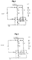
- the main principle is that a capacitor C1 is charged, when the reset means is actuated. However, charging is only to take place on condition that the monitored stop relays K1 and K2 have fallen. If this is the case and if the reset means is actuated (pressed), the current path is closed from the positive voltage supply indicated in the uppermost portion of the drawing via the contacts 1, 2 of the reset means PB1 and the relay contacts K1 and K2 down to the positive side of the capacitor C1.
- the negative side of the capacitor C1 is connected to the anode of a diode V1, the cathode of which is connected to the zero conductor (or negative supply conductors indicated as "0 V" in the lowermost portion of the drawing.
- the capacitor C1 is supplied with electrical energy, as long as the reset means PB1 is activated.
- the diode V1 establishes a virtual zero point between the capacitor C1 and the actual zero conductor. Furthermore, the diode V1 forms a common node for the capacitor C1 and the relays K1 and K2, respectively, which according to the following are activated during the reset procedure.
- the electrical charges stored in capacitor C1 are conducted from the positive side of the capacitor through the contacts 3 and 4 of the reset means PB1, the zero conductor and a second diode V2 to the relay coils in K1 and K2 and then to the negative side of the capacitor C1.
- This closed discharge current loop is illustrated by way of a dashed line provided with arrows in FIG 3.
- the diode V1 prevents the discharge procedure from occurring directly from the zero conductor up to the negative side of capacitor C1. Therefore, the charges are conducted from capacitor C1 through the diode V2 and the relay coils K1 and K2 to the negative side of capacitor C1, relays K1 and K2 thereby pulling. Once they have pulled, they are able to self-energize through any of their closing contacts (in the drawing: K1), on condition that the input In A is closed.
- the components comprised in the reset circuit must be actively supervised. If for instance a short circuit arises in diode V1, the discharge procedure when the reset means PB1 is released will occur directly through PB1, a short distance of the zero conductor and then through the shorted diode V1 directly back to the negative side of capacitor C1, and therefore no current will flow through the relay coils K1 and K2, respectively, and the relay contacts will be prevented from closing.
- the capacitor C1 cannot be charged, when the reset means PB1 is activated, since the current from the negative side of capacitor C1 cannot run through diode V1 nor from the "reverse side” through the relay coils K1 and K2, thanks to the reverse-biassed diode V2.
- diode V2 is the subject of a short circuit
- a shorted diode V2 will prevent the relays K1 and K2 from being self-energized through the closed input In A, since the current will be conducted past the relays K1, K2 via the shorted diode V2.
- V2 would be subjected to an open circuit, the circuitry according to FIGs 1-3 will prevent unintentional reset, since the discharge path will also be interrupted.
- a supervised reset function is provided in a safety relay at a minimum of components and costs (particularly at a minimum of relays), wherein the risk of malfunctions (unintentional reset) due to a short circuit or an open circuit in any used component has been eliminated by establishing a controlled discharge path to the stop relays through the zero conductor.
- FIG 4 there is shown a reset circuit for a safety relay with two inputs In A and In B.
- the same reference numerals as in the preceding figures are used for the same or corresponding components.
- the reset circuit of FIG 4 is fully semiconductor-based, which gives considerable advantages from a manufacturing point of view.
- the reset procedure starts by activating the reset means PB1.
- PB1, K1, K2 On condition that the relays K1 and K2 have fallen, a charging current will be conducted from the positive voltage supply via PB1, K1, K2 and a diode V4 down to the posivite side of the capacitor C1.
- the negative side of C1 is connected to the second voltage supply conductor (the zero conductor) via the diode V1. Similar to the above a closed current loop will be generated as a consequence, wherein the capacitor C1 is charged.
- a bipolar PNP transistor V5 is arranged as a valve for controlling the charging and discharging paths, respectively.
- the base terminal of the PNP transistor V5 is connected to a resistor R2, which in turn is connected to a resistor R1 as well as a common node between the relay contacts K1, K2 and the anode of the diode V4.
- the emitter terminal of V5 is connected to a common node between the cathode of the diode V4 and the positive side of the capacitor C1, while the collector terminal is directly connected to the zero conductor. In the charging state the PNP transistor V5 is cut off and no current flows through it.
- the PNP transistor V5 switches to its conductive state, wherein the electrical energy stored in capacitor C1 may start flowing as an electrical current from the positive side of C1, through the transistor V5 and down to the zero conductor.
- the relays K1, K2 will pull, and they may subsequently energize themselves through their closing contacts, provided that the inputs In A and In B, respectively, are closed.
- the embodiment described above has an advantage in that it allows a realization of the reset circuit, which is completely free from relays (obviously with the exception of the stop relays K1, K2).
- the semiconductor-based reset circuit may preferably be realized as a hybride circuit.
- Another advantage is that several channels/inputs (here: two) may be served by one single capacitor circuit, i.e. the leftmost portion of the circuit diagram remains the same regardless of whether the safety relay has one or more than one channel.
- stop relays K1 and K2 require relatively large currents - and consequently also high voltages - in order to pull, it is desired to minimize the voltage drops in the reset circuit according to preceding figures.
- One possibility is to use low voltage-drop diodes, such as Schottky diodes (voltage drop ⁇ 0.1 V). However, sometimes this is not enough in reality, for instance due to long wires.
- An alternative embodiment of the present invention solves the problem of insufficient voltages by way of a voltage doubling function, which will be described in more detail below with reference to FIGS 5 and 6.
- FIG 5 illustrates an embodiment, which is particularly directed at solving the problem described above as regards undervoltages and long wires.
- the arrangement of FIG 5 has one channel, but the principle is applicable in all essential details also to multiple channels, such as two channels.
- FIG 5 illustrates a relay-based reset circuit with a switching relay K3.
- the stop relays K1 and K2, the reset means PB1, the input In A and the diodes V1 and V2 correspond to the corresponding components in previous figures and are therefore not described in more detail now.
- the relay coil K3 is connected in series with PB1 between the two supply conductors, and when PB1 is activated, a closed current path is formed from the positive supply, via the relay contacts K1, K2 and K3 (since the relay contact K3 assumes its pulled position), down through a diode V3, across capacitor C1 and further down through the diode V1 to the zero conductor.
- the capacitor C1 is charged in the way described above.
- a second capacitor C2 is arranged in the reset circuit. A positive side of C2 is connected to the anode of V3, while the negative side connects to the zero conductor via the closing relay contact K3. Therefore, capacitor C2 is charged simultaneously with capacitor C1.
- relay K3 will fall, wherein the relay contact K3 assumes its second position and wherein the charging of C1 and C2 ceases. Instead a discharge path is formed from the positive side of C1 via the relay contact K3 to the negative side of C2, and then from the positive side thereof via the relay contact K3 in its position according to the figure down to the zero conductor. The current continues to flow from this conductor in a normal way through diode V2 to the relay coils K1, K2, which are able to pull. Hence, the two capacitors C1, C2 are discharged in series with each other, which means that the drive voltage available for resetting the safety relay is doubled - provided that the two capacitors are of equal capacitance.
- relays Since relays have an inherent hysteresis - they may require for instance 16 V to pull but then only e.g. 5 V for self-energizing - the doubled voltage gives a substantially improved opportunity, at the moment of reset, to overcome any existing problems with undervoltages.
- FIG 6 illustrates a semiconductor-based embodiment with a voltage doubling function corresponding to that of FIG 5.
- the rightmost portion of the circuit diagram, i.e. the relays K1 and K2, the diodes V1, V2, and V3, and the capacitor C1, corresponds fully to FIG 5.
- the difference for FIG 6 is that a semiconductor-based circuitry is provided as replacement for the relay K3.
- Two PNP transistors V6, V8 play an active part, together with an NPN transistor V7, during the reset procedure briefly described below.
- the capacitor C1 is charged as described above through diodes V3 and V1.
- the transistors V6 and V8 are cut off in this moment, while transistor V7 is conductive, wherein a current path parallel to said charging path is formed through the second capacitor C2 via the diode V5 and the transistor V7.
- the transistor V7 When the activation of the reset means PB1 ends, the transistor V7 is cut off and transistors V6 and V8 start to conduct.
- a discharge path is formed starting from the positive side of capacitor C1, through transistor V6 and further to the negative side of the capacitor C2. From the positive side of the capacitor C2 the discharge current flows from the transistor V8, down to the zero conductor and up through diode V2 to the relay coils K1, K2. In the way described above the relay coils K1, K2 are hence supplied with current, thereby causing them to pull and then to self-energize.
- the transistors V6 and V8 are conductive simultaneously, the capacitors C1 and C2 are connected in series with each other during the discharge, wherein a voltage doubling is achieved and hence a considerably improved opportunity of a successful reset of the safety relay, despite any problems with undervoltages.
- FIG 7 The circuit of FIG 7 is based on the semiconductor version of a two-channel safety relay of FIG 4. All components and functions are identical to those of FIG 4, except for what is mentioned below.
- a second PNP transistor V6 is at its emitter terminal connected to the series connection PB1-K1-K2, while the collector terminal of V6 connects to the anode of diode V4 and to the input of a hysteresis circuit H1, which is symbolically represented by an inverter labelled with a hysteresis sign.
- the output of the hysteresis circuit H1 is connected to the base input of a third PNP transistor V7, the emitter of which is connected to an autostart input.
- the collector terminal of V7 is connected to the base terminal of the second PNP transistor V6 and to the zero conductor via a resistor R3.
- the embodiment of FIG 7 is arranged to reset the safety relay, when the reset input PB1 is closed, on condition that the autostart input is connected to the voltage supply, either by direct connection to the positive supply conductor or by indirect connection via a clamp between the autostart input and PB1.
- the hysteresis circuit H1 will detect the charge level of the capacitor C1. Once the charge exceeds a first limit, the output of the hysteresis circuit H1 will go low, causing the transistor V7 to open and the transistor V5 to be cut off.
- the reset circuit will switch to its discharge state, wherein the capacitor C1 is discharged through the transistor V5, the zero conductor, the diodes V2 and V3 and the relay coils Ki and K2, which will pull.
- the hysteresis circuit H1 will switch again, causing the reset circuit to enter a passive idle mode awaiting a forthcoming need for reset due to closed inputs In A, In B, fallen relay contacts K1, K2, etc.
- the hysteresis circuit H1 which has been schematically illustrated herein in the form of an inverter with hysteresis properties, may be realized in a suitable way depending on application.
- To realize a hysteresis circuit with the functionality described above is regarded to be within the field of competence of a skilled person. The important condition to fulfil is that the circuit will actually be given sufficient hysteresis properties, so that oscillation is avoided.
- H1 may be arranged to operate according to a time measuring approach. First, H1 will maintain the reset circuit in the charging state according to the above. Once capacitor C1 has reached a certain amount of charging, H1 will be triggered, wherein the reset circuit is maintained in its discharge state during a predetermined time period, which preferably corresponds to the discharge time of capacitor C1. Then the reset circuit will switch to its normal state.
- the circuit H1 may first maintain the reset circuit in its charge state during a first predetermined time period, preferably corresponding to the time it takes to charge C1 up to a certain level. Thereinafter the circuit H1 will switch to a second state, wherein the capacitor C1 is discharged during a second predetermined time period.
- the diode V2 (and for some embodiments also its parallel diode V3), which is used in all embodiments, may alternatively be realized as a thyristor.
- a thyristor has an advantage in that an external switch, such as an optoswitch, may be connected to the control input of the thyristor, wherein an additional dimension of safety is obtained. If this external switch does not supply an expected control signal to the thyristor (because the external switch has detected an abnormal condition, such as an opened safety gate, etc), the thyristor will not operate normally, wherein unintentional reset is prevented in correspondence with the reasoning for the embodiment of FIGs 1-3. Furthermore, the thyristor and the separate opto-switch may be replaced by an optothyristor.
- the bipolar transistors may be replaced by for instance field effect transistors, while the diodes may be replaced by transistors connected as diodes, etc.
- stop relays K1, K2 described in the embodiments above may alternatively be realized as a single relay with only one relay coil but two independent contact halves, wherein each contact half comprises at least one closing and one opening relay contact, which are connected in a controlled arrangement.
- Such a relay may, at least in simple applications, therefore replace the function of the double stop relays K1, K2 disclosed in the drawings with preserved safety.
Landscapes
- Relay Circuits (AREA)
- Control Of Combustion (AREA)
- Air Bags (AREA)
- Safety Devices In Control Systems (AREA)
Applications Claiming Priority (3)
| Application Number | Priority Date | Filing Date | Title |
|---|---|---|---|
| SE9604520 | 1996-12-09 | ||
| SE9604520A SE509479C2 (sv) | 1996-12-09 | 1996-12-09 | Säkerhetsrelä och sätt vid återställning av ett säkerhetsrelä |
| PCT/SE1997/001995 WO1998028764A1 (en) | 1996-12-09 | 1997-11-28 | Safety relay |
Publications (2)
| Publication Number | Publication Date |
|---|---|
| EP0944911A1 EP0944911A1 (en) | 1999-09-29 |
| EP0944911B1 true EP0944911B1 (en) | 2000-08-16 |
Family
ID=20404904
Family Applications (1)
| Application Number | Title | Priority Date | Filing Date |
|---|---|---|---|
| EP97948064A Expired - Lifetime EP0944911B1 (en) | 1996-12-09 | 1997-11-28 | Safety relay |
Country Status (9)
| Country | Link |
|---|---|
| US (1) | US6236553B1 (da) |
| EP (1) | EP0944911B1 (da) |
| JP (1) | JP4060369B2 (da) |
| AT (1) | ATE195608T1 (da) |
| AU (1) | AU5421098A (da) |
| DE (2) | DE69702869T2 (da) |
| DK (1) | DK0944911T3 (da) |
| SE (1) | SE509479C2 (da) |
| WO (1) | WO1998028764A1 (da) |
Families Citing this family (11)
| Publication number | Priority date | Publication date | Assignee | Title |
|---|---|---|---|---|
| DE10037383A1 (de) * | 2000-08-01 | 2002-02-21 | Pilz Gmbh & Co | Sicherheitsschaltgerät zum sicheren Abschalten eines elektrischen Verbrauchers, insbesondere einer elektrisch angetriebenen Maschine |
| US6856490B2 (en) * | 2002-02-07 | 2005-02-15 | Seagate Technology Llc | Flex cable assembly with improved flex cable dynamic loop characteristics |
| WO2006008781A1 (ja) * | 2004-05-26 | 2006-01-26 | Mitsubishi Denki Kabushiki Kaisha | 接点開閉器 |
| JP2007263446A (ja) * | 2006-03-28 | 2007-10-11 | Miura Co Ltd | 機器 |
| DE102008002758B4 (de) * | 2008-01-25 | 2016-04-28 | Schneider Electric Automation Gmbh | Relaisschaltung |
| US8576074B2 (en) * | 2009-06-22 | 2013-11-05 | General Atomics | Charged capacitor warning system and method |
| US8720481B2 (en) * | 2011-10-13 | 2014-05-13 | Kevin Duane Guy | Fluid leak detection and shutdown apparatus |
| US9155232B2 (en) * | 2013-01-10 | 2015-10-06 | Rockwell Automation Technologies, Inc. | Wide input voltage range power supply circuit |
| US9618909B2 (en) | 2013-12-20 | 2017-04-11 | Thales Canada Inc | Safety assurance of multiple redundant systems |
| JP2017196714A (ja) * | 2016-04-28 | 2017-11-02 | セイコーエプソン株式会社 | ロボット用装置、ロボット制御装置、及びロボットシステム |
| US20240198528A1 (en) * | 2022-12-15 | 2024-06-20 | The Boeing Company | Apparatus and methods to reduce impact of robot collision and/or avoid robot collision |
Family Cites Families (7)
| Publication number | Priority date | Publication date | Assignee | Title |
|---|---|---|---|---|
| US3749005A (en) * | 1971-09-30 | 1973-07-31 | Danly Machine Corp | Electrical control system for a power press |
| SE465067B (sv) | 1988-03-24 | 1991-07-22 | Jokab Safety Ab | Anordning vid produktionsanpassade skyddssystem |
| JPH0261930A (ja) | 1988-08-26 | 1990-03-01 | Matsushita Electric Works Ltd | リレー駆動回路 |
| US5079667A (en) * | 1989-01-26 | 1992-01-07 | Matsushita Electric Works, Ltd. | Relay driving circuit for a latch-in relay |
| DE4413637C1 (de) * | 1994-04-20 | 1995-07-27 | Schmidt Feinmech | Fehlersichere Schaltung |
| US5689398A (en) * | 1996-01-03 | 1997-11-18 | Allen-Bradley Company, Inc. | Redundant control relay circuits |
| SE504673C2 (sv) * | 1996-02-23 | 1997-03-24 | Ross Operating Valve Co | Återinkopplingsspärr för ett i varje arbetscykel självkontrollerande styrdon |
-
1996
- 1996-12-09 SE SE9604520A patent/SE509479C2/sv not_active IP Right Cessation
-
1997
- 1997-11-28 US US09/319,224 patent/US6236553B1/en not_active Expired - Lifetime
- 1997-11-28 DE DE69702869T patent/DE69702869T2/de not_active Expired - Lifetime
- 1997-11-28 JP JP52597298A patent/JP4060369B2/ja not_active Expired - Lifetime
- 1997-11-28 WO PCT/SE1997/001995 patent/WO1998028764A1/en not_active Ceased
- 1997-11-28 AU AU54210/98A patent/AU5421098A/en not_active Abandoned
- 1997-11-28 EP EP97948064A patent/EP0944911B1/en not_active Expired - Lifetime
- 1997-11-28 DK DK97948064T patent/DK0944911T3/da active
- 1997-11-28 DE DE0944911T patent/DE944911T1/de active Pending
- 1997-11-28 AT AT97948064T patent/ATE195608T1/de not_active IP Right Cessation
Also Published As
| Publication number | Publication date |
|---|---|
| SE9604520L (sv) | 1998-06-10 |
| DE944911T1 (de) | 2000-03-09 |
| AU5421098A (en) | 1998-07-17 |
| JP2001506050A (ja) | 2001-05-08 |
| EP0944911A1 (en) | 1999-09-29 |
| US6236553B1 (en) | 2001-05-22 |
| SE9604520D0 (sv) | 1996-12-09 |
| DE69702869T2 (de) | 2001-04-05 |
| ATE195608T1 (de) | 2000-09-15 |
| SE509479C2 (sv) | 1999-02-01 |
| DK0944911T3 (da) | 2000-12-18 |
| WO1998028764A1 (en) | 1998-07-02 |
| DE69702869D1 (de) | 2000-09-21 |
| JP4060369B2 (ja) | 2008-03-12 |
Similar Documents
| Publication | Publication Date | Title |
|---|---|---|
| EP2426803B1 (en) | Protection circuit for a power conversion apparatus | |
| CN101931218B (zh) | 与母线连接的组件供电电流电子监控装置 | |
| EP3657630B1 (en) | Fault handling method and device for power supply device | |
| EP0944911B1 (en) | Safety relay | |
| CN100536056C (zh) | 用于故障保险地断开电负载的安全开关装置及相应的方法 | |
| US9852852B2 (en) | Safety switching apparatus with switching element in the auxiliary contact current path | |
| JP2015513885A (ja) | 電源装置付き安全開閉装置 | |
| MXPA06010471A (es) | Dispositivo de disparo electronico equipado con medios de monitoreo, interruptor de circuito que comprende dicho dispositivo de disparo y metodo de monitoreo. | |
| TWI534579B (zh) | 電力供給控制裝置,及可程式邏輯控制器 | |
| CS277638B6 (en) | Circuit arrangement for checking of a for power transistor switching state | |
| US20220006291A1 (en) | Switching device for safely disconnecting an electrical load from a power supply network and a safety switching system | |
| US3571659A (en) | Switching device for power supply circuit | |
| CA2333483A1 (en) | Device for safely disconnecting an electrical load | |
| US6809911B2 (en) | Safety switching device for safely switching off an electrical load | |
| US20090190282A1 (en) | Relay connection | |
| JP4176185B2 (ja) | 監視回路 | |
| JP7697060B2 (ja) | 制御装置および加工機器 | |
| EP4113226B1 (en) | Current limiting circuit for i/o modules | |
| US5825102A (en) | Fail-safe circuit | |
| US12235320B2 (en) | Safety switching apparatus, in particular for the monitored switching on of an electrical and/or electronic load | |
| JP2018182962A (ja) | モータ制御装置 | |
| CN108983594B (zh) | 安全接通和/或断开至少一台机器的模块化安全继电器电路 | |
| EP4119400B1 (en) | Power supply management system for a vehicle | |
| EP4456361B1 (en) | Switch control device and battery pack including the same | |
| JP7849285B2 (ja) | 組電池制御装置、組電池制御方法、及び蓄電システム |
Legal Events
| Date | Code | Title | Description |
|---|---|---|---|
| ITCL | It: translation for ep claims filed |
Representative=s name: JACOBACCI CASETTA & PERANI S.P.A. |
|
| PUAI | Public reference made under article 153(3) epc to a published international application that has entered the european phase |
Free format text: ORIGINAL CODE: 0009012 |
|
| 17P | Request for examination filed |
Effective date: 19981223 |
|
| AK | Designated contracting states |
Kind code of ref document: A1 Designated state(s): AT BE CH DE DK ES FI FR GB GR IE IT LI LU MC NL PT SE |
|
| GRAG | Despatch of communication of intention to grant |
Free format text: ORIGINAL CODE: EPIDOS AGRA |
|
| 17Q | First examination report despatched |
Effective date: 19991019 |
|
| GRAG | Despatch of communication of intention to grant |
Free format text: ORIGINAL CODE: EPIDOS AGRA |
|
| GRAH | Despatch of communication of intention to grant a patent |
Free format text: ORIGINAL CODE: EPIDOS IGRA |
|
| DET | De: translation of patent claims | ||
| GRAH | Despatch of communication of intention to grant a patent |
Free format text: ORIGINAL CODE: EPIDOS IGRA |
|
| GRAA | (expected) grant |
Free format text: ORIGINAL CODE: 0009210 |
|
| AK | Designated contracting states |
Kind code of ref document: B1 Designated state(s): AT BE CH DE DK ES FI FR GB GR IE IT LI LU MC NL PT SE |
|
| PG25 | Lapsed in a contracting state [announced via postgrant information from national office to epo] |
Ref country code: NL Free format text: LAPSE BECAUSE OF FAILURE TO SUBMIT A TRANSLATION OF THE DESCRIPTION OR TO PAY THE FEE WITHIN THE PRESCRIBED TIME-LIMIT Effective date: 20000816 Ref country code: LI Free format text: LAPSE BECAUSE OF FAILURE TO SUBMIT A TRANSLATION OF THE DESCRIPTION OR TO PAY THE FEE WITHIN THE PRESCRIBED TIME-LIMIT Effective date: 20000816 Ref country code: GR Free format text: LAPSE BECAUSE OF NON-PAYMENT OF DUE FEES Effective date: 20000816 Ref country code: FI Free format text: LAPSE BECAUSE OF FAILURE TO SUBMIT A TRANSLATION OF THE DESCRIPTION OR TO PAY THE FEE WITHIN THE PRESCRIBED TIME-LIMIT Effective date: 20000816 Ref country code: ES Free format text: THE PATENT HAS BEEN ANNULLED BY A DECISION OF A NATIONAL AUTHORITY Effective date: 20000816 Ref country code: CH Free format text: LAPSE BECAUSE OF FAILURE TO SUBMIT A TRANSLATION OF THE DESCRIPTION OR TO PAY THE FEE WITHIN THE PRESCRIBED TIME-LIMIT Effective date: 20000816 Ref country code: BE Free format text: LAPSE BECAUSE OF FAILURE TO SUBMIT A TRANSLATION OF THE DESCRIPTION OR TO PAY THE FEE WITHIN THE PRESCRIBED TIME-LIMIT Effective date: 20000816 Ref country code: AT Free format text: LAPSE BECAUSE OF FAILURE TO SUBMIT A TRANSLATION OF THE DESCRIPTION OR TO PAY THE FEE WITHIN THE PRESCRIBED TIME-LIMIT Effective date: 20000816 |
|
| REF | Corresponds to: |
Ref document number: 195608 Country of ref document: AT Date of ref document: 20000915 Kind code of ref document: T |
|
| REG | Reference to a national code |
Ref country code: CH Ref legal event code: EP |
|
| REG | Reference to a national code |
Ref country code: IE Ref legal event code: FG4D |
|
| REF | Corresponds to: |
Ref document number: 69702869 Country of ref document: DE Date of ref document: 20000921 |
|
| ITF | It: translation for a ep patent filed | ||
| PG25 | Lapsed in a contracting state [announced via postgrant information from national office to epo] |
Ref country code: SE Free format text: LAPSE BECAUSE OF FAILURE TO SUBMIT A TRANSLATION OF THE DESCRIPTION OR TO PAY THE FEE WITHIN THE PRESCRIBED TIME-LIMIT Effective date: 20001116 Ref country code: PT Free format text: LAPSE BECAUSE OF FAILURE TO SUBMIT A TRANSLATION OF THE DESCRIPTION OR TO PAY THE FEE WITHIN THE PRESCRIBED TIME-LIMIT Effective date: 20001116 |
|
| PG25 | Lapsed in a contracting state [announced via postgrant information from national office to epo] |
Ref country code: LU Free format text: LAPSE BECAUSE OF NON-PAYMENT OF DUE FEES Effective date: 20001128 Ref country code: IE Free format text: LAPSE BECAUSE OF NON-PAYMENT OF DUE FEES Effective date: 20001128 |
|
| PG25 | Lapsed in a contracting state [announced via postgrant information from national office to epo] |
Ref country code: MC Free format text: THE PATENT HAS BEEN ANNULLED BY A DECISION OF A NATIONAL AUTHORITY Effective date: 20001130 |
|
| ET | Fr: translation filed | ||
| REG | Reference to a national code |
Ref country code: DK Ref legal event code: T3 |
|
| RAP2 | Party data changed (patent owner data changed or rights of a patent transferred) |
Owner name: JOKAB SAFETY AB |
|
| REG | Reference to a national code |
Ref country code: CH Ref legal event code: PL |
|
| PLBI | Opposition filed |
Free format text: ORIGINAL CODE: 0009260 |
|
| 26 | Opposition filed |
Opponent name: GEORG VONDRACEK DIPL. ING. Effective date: 20010313 |
|
| REG | Reference to a national code |
Ref country code: GB Ref legal event code: 732E |
|
| PLBF | Reply of patent proprietor to notice(s) of opposition |
Free format text: ORIGINAL CODE: EPIDOS OBSO |
|
| REG | Reference to a national code |
Ref country code: IE Ref legal event code: MM4A |
|
| REG | Reference to a national code |
Ref country code: FR Ref legal event code: ST |
|
| PLBF | Reply of patent proprietor to notice(s) of opposition |
Free format text: ORIGINAL CODE: EPIDOS OBSO |
|
| REG | Reference to a national code |
Ref country code: GB Ref legal event code: IF02 |
|
| REG | Reference to a national code |
Ref country code: FR Ref legal event code: RN |
|
| PLBO | Opposition rejected |
Free format text: ORIGINAL CODE: EPIDOS REJO |
|
| PLBN | Opposition rejected |
Free format text: ORIGINAL CODE: 0009273 |
|
| STAA | Information on the status of an ep patent application or granted ep patent |
Free format text: STATUS: OPPOSITION REJECTED |
|
| 27O | Opposition rejected |
Effective date: 20020328 |
|
| PGFP | Annual fee paid to national office [announced via postgrant information from national office to epo] |
Ref country code: DK Payment date: 20031114 Year of fee payment: 7 |
|
| PGFP | Annual fee paid to national office [announced via postgrant information from national office to epo] |
Ref country code: GB Payment date: 20031125 Year of fee payment: 7 |
|
| PGFP | Annual fee paid to national office [announced via postgrant information from national office to epo] |
Ref country code: FR Payment date: 20031128 Year of fee payment: 7 |
|
| PG25 | Lapsed in a contracting state [announced via postgrant information from national office to epo] |
Ref country code: GB Free format text: LAPSE BECAUSE OF NON-PAYMENT OF DUE FEES Effective date: 20041128 |
|
| PG25 | Lapsed in a contracting state [announced via postgrant information from national office to epo] |
Ref country code: DK Free format text: LAPSE BECAUSE OF NON-PAYMENT OF DUE FEES Effective date: 20041130 |
|
| REG | Reference to a national code |
Ref country code: DK Ref legal event code: EBP |
|
| GBPC | Gb: european patent ceased through non-payment of renewal fee |
Effective date: 20041128 |
|
| PG25 | Lapsed in a contracting state [announced via postgrant information from national office to epo] |
Ref country code: FR Free format text: LAPSE BECAUSE OF NON-PAYMENT OF DUE FEES Effective date: 20050729 |
|
| REG | Reference to a national code |
Ref country code: FR Ref legal event code: ST |
|
| PG25 | Lapsed in a contracting state [announced via postgrant information from national office to epo] |
Ref country code: IT Free format text: LAPSE BECAUSE OF NON-PAYMENT OF DUE FEES Effective date: 20051128 |
|
| REG | Reference to a national code |
Ref country code: DE Ref legal event code: R082 Ref document number: 69702869 Country of ref document: DE Representative=s name: KADOR & PARTNER, DE |
|
| REG | Reference to a national code |
Ref country code: DE Ref legal event code: R082 Ref document number: 69702869 Country of ref document: DE Representative=s name: KADOR & PARTNER PARTG MBB PATENTANWAELTE, DE Effective date: 20150512 Ref country code: DE Ref legal event code: R082 Ref document number: 69702869 Country of ref document: DE Representative=s name: KADOR & PARTNER PART MBB PATENTANWAELTE, DE Effective date: 20150512 Ref country code: DE Ref legal event code: R082 Ref document number: 69702869 Country of ref document: DE Representative=s name: KADOR & PARTNER PARTG MBB, DE Effective date: 20150512 Ref country code: DE Ref legal event code: R082 Ref document number: 69702869 Country of ref document: DE Representative=s name: KADOR & PARTNER, DE Effective date: 20150512 Ref country code: DE Ref legal event code: R081 Ref document number: 69702869 Country of ref document: DE Owner name: ABB SCHWEIZ AG, CH Free format text: FORMER OWNER: JOKAB SAFETY AB, MALMOE, SE Effective date: 20150512 Ref country code: DE Ref legal event code: R081 Ref document number: 69702869 Country of ref document: DE Owner name: ABB TECHNOLOGY LTD., CH Free format text: FORMER OWNER: JOKAB SAFETY AB, MALMOE, SE Effective date: 20150512 |
|
| PGFP | Annual fee paid to national office [announced via postgrant information from national office to epo] |
Ref country code: DE Payment date: 20161121 Year of fee payment: 20 |
|
| REG | Reference to a national code |
Ref country code: DE Ref legal event code: R082 Ref document number: 69702869 Country of ref document: DE Representative=s name: KADOR & PARTNER PARTG MBB PATENTANWAELTE, DE Ref country code: DE Ref legal event code: R082 Ref document number: 69702869 Country of ref document: DE Representative=s name: KADOR & PARTNER PART MBB PATENTANWAELTE, DE Ref country code: DE Ref legal event code: R082 Ref document number: 69702869 Country of ref document: DE Representative=s name: KADOR & PARTNER PARTG MBB, DE Ref country code: DE Ref legal event code: R081 Ref document number: 69702869 Country of ref document: DE Owner name: ABB SCHWEIZ AG, CH Free format text: FORMER OWNER: ABB TECHNOLOGY LTD., ZUERICH, CH |
|
| REG | Reference to a national code |
Ref country code: DE Ref legal event code: R071 Ref document number: 69702869 Country of ref document: DE |