EP0945733A2 - Zerstörungsfreies Verfahren zur Bestimmung der Minoritätsträger-Diffusionslänge und Lebensdauer im Halbleitervorrichtungen - Google Patents
Zerstörungsfreies Verfahren zur Bestimmung der Minoritätsträger-Diffusionslänge und Lebensdauer im Halbleitervorrichtungen Download PDFInfo
- Publication number
- EP0945733A2 EP0945733A2 EP99105753A EP99105753A EP0945733A2 EP 0945733 A2 EP0945733 A2 EP 0945733A2 EP 99105753 A EP99105753 A EP 99105753A EP 99105753 A EP99105753 A EP 99105753A EP 0945733 A2 EP0945733 A2 EP 0945733A2
- Authority
- EP
- European Patent Office
- Prior art keywords
- semiconductor device
- minority carrier
- length
- isignal
- dut
- Prior art date
- Legal status (The legal status is an assumption and is not a legal conclusion. Google has not performed a legal analysis and makes no representation as to the accuracy of the status listed.)
- Withdrawn
Links
Images


Classifications
-
- G—PHYSICS
- G01—MEASURING; TESTING
- G01R—MEASURING ELECTRIC VARIABLES; MEASURING MAGNETIC VARIABLES
- G01R31/00—Arrangements for testing electric properties; Arrangements for locating electric faults; Arrangements for electrical testing characterised by what is being tested not provided for elsewhere
- G01R31/28—Testing of electronic circuits, e.g. by signal tracer
- G01R31/302—Contactless testing
- G01R31/308—Contactless testing using non-ionising electromagnetic radiation, e.g. optical radiation
- G01R31/311—Contactless testing using non-ionising electromagnetic radiation, e.g. optical radiation of integrated circuits
-
- H—ELECTRICITY
- H10—SEMICONDUCTOR DEVICES; ELECTRIC SOLID-STATE DEVICES NOT OTHERWISE PROVIDED FOR
- H10P—GENERIC PROCESSES OR APPARATUS FOR THE MANUFACTURE OR TREATMENT OF DEVICES COVERED BY CLASS H10
- H10P74/00—Testing or measuring during manufacture or treatment of wafers, substrates or devices
-
- G—PHYSICS
- G01—MEASURING; TESTING
- G01R—MEASURING ELECTRIC VARIABLES; MEASURING MAGNETIC VARIABLES
- G01R31/00—Arrangements for testing electric properties; Arrangements for locating electric faults; Arrangements for electrical testing characterised by what is being tested not provided for elsewhere
- G01R31/26—Testing of individual semiconductor devices
- G01R31/265—Contactless testing
- G01R31/2656—Contactless testing using non-ionising electromagnetic radiation, e.g. optical radiation
-
- G—PHYSICS
- G01—MEASURING; TESTING
- G01R—MEASURING ELECTRIC VARIABLES; MEASURING MAGNETIC VARIABLES
- G01R31/00—Arrangements for testing electric properties; Arrangements for locating electric faults; Arrangements for electrical testing characterised by what is being tested not provided for elsewhere
- G01R31/26—Testing of individual semiconductor devices
- G01R31/2648—Characterising semiconductor materials
-
- G—PHYSICS
- G01—MEASURING; TESTING
- G01R—MEASURING ELECTRIC VARIABLES; MEASURING MAGNETIC VARIABLES
- G01R31/00—Arrangements for testing electric properties; Arrangements for locating electric faults; Arrangements for electrical testing characterised by what is being tested not provided for elsewhere
- G01R31/28—Testing of electronic circuits, e.g. by signal tracer
- G01R31/282—Testing of electronic circuits specially adapted for particular applications not provided for elsewhere
- G01R31/2831—Testing of materials or semi-finished products, e.g. semiconductor wafers or substrates
-
- H—ELECTRICITY
- H10—SEMICONDUCTOR DEVICES; ELECTRIC SOLID-STATE DEVICES NOT OTHERWISE PROVIDED FOR
- H10P—GENERIC PROCESSES OR APPARATUS FOR THE MANUFACTURE OR TREATMENT OF DEVICES COVERED BY CLASS H10
- H10P74/00—Testing or measuring during manufacture or treatment of wafers, substrates or devices
- H10P74/20—Testing or measuring during manufacture or treatment of wafers, substrates or devices characterised by the properties tested or measured, e.g. structural or electrical properties
- H10P74/207—Electrical properties, e.g. testing or measuring of resistance, deep levels or capacitance-voltage characteristics
Definitions
- This invention relates to a method for measuring by means of an optical beam induced current (OBIC), or by an electron beam induced current (EBIC), minority carrier diffusion length and minority carrier lifetime in various semiconductor devices, such as lateral double diffused metal oxide semiconductors (LDMOS) which are intended for higher voltage (HV) applications, as well as other semiconductor devices including metal oxide semiconductor field effect transistors (MOSFET), and ultra-miniature dynamic random access memories (DRAM).
- OBIC optical beam induced current
- EBIC electron beam induced current
- minority carrier diffusion length minority carrier diffusion length and minority carrier lifetime in various semiconductor devices, such as lateral double diffused metal oxide semiconductors (LDMOS) which are intended for higher voltage (HV) applications, as well as other semiconductor devices including metal oxide semiconductor field effect transistors (MOSFET), and ultra-miniature dynamic random access memories (DRAM).
- OBIC optical beam induced current
- EBIC electron beam induced current
- MOSFET metal oxide semiconductor field effect transistors
- DRAM ultra-miniature dynamic random access memories
- an induced current can be generated in a semiconductor having a p-n junction or Schottky barrier (metal-semiconductor rectifying contact) by shining a focused beam of radiation of above bandgap energy, either optical or electron beam, on the body of the semiconductor.
- Apparatus for generating such beams and for scanning them across a device under test (DUT) are commercially available. Where a DUT is small (e.g., smaller than a micron), a scanning electron microscope utilizing an electron beam and vacuum chamber is typically used to investigate the device.
- a laser beam shining through an optical microscope to illuminate and scan the device.
- Such laser-optical apparatus is also commercially available. But in either case, when a semiconductor with a p-n junction is illuminated by a radiant beam of appropriate wavelength and intensity, a small current is generated in the semiconductor. In the case of an electron beam, current is generated by the "Compton effect". For a laser beam, current is due to the photo effect. Both of these effects are well known.
- a problem prior to this invention was how to quantitatively measure in a nondestructive way the degradation of materials of a semiconductor device caused by process-induced defects, such as dislocations, oxidation induced stacking faults (OSFS), thermal and stress induced slip, misfit, point defect agglomeration and precipitation, bulk micro defects (BMDs), etc.
- Minority carrier lifetime is a good measure of the overall quality of semiconductor material, such as a wafer of silicon (Si). After a number of wafer processing steps (e.g., a hundred or more steps) and thermal cyclings, such as during annealing at above 900°C or so, process-induced defects may be nucleated and generated in devices being fabricated on the wafer.
- the recombination properties of minority carriers determine the basic electronic properties of Si and silicon-on-insulator (SOI) materials and control the performance of a variety of Si and SOI devices. It is thus desirable to be able to measure easily, accurately and in a nondestructive way the minority carrier recombination characteristics of such devices. It is highly important to be able to do so for the proper and rapid evaluation of new Si and SOI technologies, where novel composite material systems are used and which may have varying degrees of crystal lattice perfection and unknown defect content.
- the present invention provides the ability for quick, accurate and nondestructive measurement of minority carrier diffusion length and minority carrier lifetime in semiconductor devices.
- Prior to the invention so far as is known, no one previously utilized either an EBIC or OBIC scanning system for the measurement of minority carrier diffusion length and/or minority carrier lifetime in semiconductor devices.
- the present invention is directed to a method for measurement of minority carrier diffusion length (L p ) and/or minority carrier lifetime ( ⁇ p ) in a semiconductor device such as a high-voltage transistor having a p-n junction between a p-type conductivity region and an n-type conductivity type region.
- the present invention is directed to a method for measurement of minority carrier diffusion (L p ) length and accordingly minority carrier lifetime ( ⁇ p ) in a semiconductor device.
- the method comprises the steps of reverse biasing the semiconductor device; scanning a focused beam of radiant energy along a length of the semiconductor device; detecting current induced in the semiconductor device by the beam as it passes point-by-point along the scanned length of the semiconductor device to generate a signal waveform (Isignal); and determining from the Isignal waveform minority carrier diffusion length (L p ) and/or minority carrier lifetime ( ⁇ p ) in the semiconductor device.
- the present invention is directed to a method for nondestructive measurement of minority carrier diffusion (L p ) length in a semiconductor device having a p-n junction between a p-type conductivity region and an n-type conductivity region.
- the method comprises the steps of reverse biasing with a voltage the semiconductor device; scanning a focused beam of radiant energy along a distance "x" of a length of the semiconductor device over the p-n junction and into one region thereof; detecting current induced in the semiconductor device by the beam as it passes point-by-point along the scanned length of the semiconductor device to generate a signal waveform (Isignal) as a function of distance "x"; and determining from the Isignal waveform minority carrier diffusion length (L p ), and/or minority carrier lifetime ( ⁇ p ) in the semiconductor device.
- Isignal signal waveform
- the present invention is directed to a method for nondestructive measurement of minority carrier diffusion (L p ) length and/or minority carrier lifetime ( ⁇ p ) in a semiconductor device, such as a high-voltage transistor having a p-n junction between a p-type conductivity region and an n-type conductivity region.
- the method comprises the steps of reverse basing with a voltage a semiconductor device; scanning a focused laser beam along a distance "x" of a length of the semiconductor device over the p-n junction and into one region of the semiconductor device; detecting optically beam induced current (OBIC) in the semicondcutor device as the beam passes in the "x" direction along the scanned length of the semiconductor device to generate a signal waveform (Isignal) as a function of distance "x"; and determining from the Isignal waveform minority carrier diffusion length L p and/or minority carrier lifetime ⁇ p in the semiconductor device.
- OBIC optically beam induced current
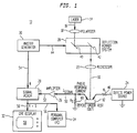
- the apparatus 10 utilizes a laser 14 which emits a beam 16, a polarizer 18, a deflection mirror system 20, a microscope 22 which focuses the beam 16 in a fine spot on the DUT 12, a device power source 24, a signal amplifier 26, a signal mixer 28, a raster generator 30, a cathode ray tube (CRT) display 32, and a personal computer (PC) 34.
- a laser 14 which emits a beam 16, a polarizer 18, a deflection mirror system 20, a microscope 22 which focuses the beam 16 in a fine spot on the DUT 12, a device power source 24, a signal amplifier 26, a signal mixer 28, a raster generator 30, a cathode ray tube (CRT) display 32, and a personal computer (PC) 34.
- PC personal computer
- the laser 14 emits a beam 16 of light with a wavelength, for example, of 633 nanometers (nm) and of suitable intensity (e.g., several watts).
- the beam 16 passes through a polarizer 18 and into the deflection mirror system 20.
- the mirror system 20 includes a plurality of moveable mirrors 40 and 42 which are driven back and forth by electrical signals received via a lead 44 from the raster generator 30. Mechanical movement of the mirrors 40 and 42 deflects the beam 16 back-and-forth and side-to-side in synchronism with electrical signals from the generator 30 as is well known to synchronize it with the CRT display.
- the beam 16 passes from the deflection mirror system 20 and into the microscope 22 which focuses the beam 16 into a fine spot (e.g., about a micron in diameter) onto a surface of the DUT 12. This results in optical beam induced current (OBIC) in the DUT 12.
- OBIC optical beam induced current
- the DUT 12 is reverse biased by a positive voltage (+V) from the device power source 24, (a negative side of which is grounded), and a load resistor (R L ) 46.
- a photo-response current passes from the DUT 12 through a sensing resistor (R s ) 48 to ground.
- a signal, termed “Isignal” is applied from the sensing resistor 48 via a lead 50 to an input of the amplifier 26, an output of which is applied via a lead 52 to one input (S) of the signal mixer 28.
- a raster signal is applied to another input (R) of the signal mixer 28 via a lead 54 from the raster generator 30.
- Dual signals (R+S) from the signal mixer 28 are applied via a common connection 56 to an input of the CRT display 32 where the signals are displayed on a screen 58 as a waveform (to be discussed hereinafter) having the usual x and y coordinates.
- the dual R+S signals on the common connection 56 are also applied to the personal computer 32 where they are processed and the minority carrier diffusion length L p and minority carrier lifetime ( ⁇ p ) are obtained, as will be explained hereinafter.
- the DUT 12 is, by way of example, an LDMOS type transistor 62 having a drain 64, a gate 65, and a source 66. It is to be understood, however, that the DUT 12 may be a semiconductor other than the transistor 62 shown here.
- the transistor 62 while being scanned by the beam 16, is reverse-biased with its drain 64 connected via the load resistor (R L ) 46 (see FIG. 1) to a positive terminal 68 (+V) of the power supply 24 (not shown here but shown in FIG. 1). A negative side of the device power supply 24 (not shown here but shown in FIG.
- the resistor (R L ) 46 may have a value of 100 K ohms
- the resistor (R S ) 48 a value of 10 K ohms
- the resistance in reverse bias across the drain 64 and the source 66 of the transistor 62 may be approximately 100M ohms.
- FIG. 3 there is shown greatly enlarged and in highly schematic and simplified form of a lateral high voltage diode, the DUT 12.
- a first shaded area of the DUT 12 represents a p+type conductivity body region 72, an unshaded area on both sides of the p-n junction 70 represents an unsymmetrical space charge region 74, and a second shaded area represents the remainder of the n-type conductivity drift region 76.
- Electrical connections to the DUT 12 are as indicated (see also FIG. 2).
- the unshaded area represents the depletion region adjacent to the p-n junction 70 of the DUT 12 where all of the laser induced photo-generated electron-hole pairs are separated and collected by the high local field applied by the reverse bias voltage, giving rise to the OBIC photocurrent.
- the second shaded area indicates a neutral n-type drift region 76 outside of the depletion region (space charge region 74) where the photo-generated carriers are not collected any more and no OBIC photocurrent is measured.
- an OBIC signal measured as Isignal (FIGS. 2 and 3) is proportional to the exponent of [ (x n - x)/L p ] or: Isignal ⁇ e [(x n - x)/L p ]
- the OBIC photocurrent (and Isignal) beyond the edge 78 of the depletion width 79 in the n-type drift region 76 varies proportionally (or nearly so) to exponent [ (X n -X)/Lp ].
- the exponential decay of the OBIC photocurrent (and Isignal) in the n-type drift region 76 within a certain number of diffusion lengths beyond the edge 78 of the depletion width is proportional to the minority carrier diffusion length Lp and consequently is a measure of the Lp of the semiconductor material from which the DUT 12 is built. This will be explained in greater detail hereinafter.
- FIG. 4 there is shown a graph 80 of a somewhat idealized waveform 82 of Isignal.
- the horizontal axis of the graph 80 represents distance in the x direction along the DUT 12 (FIG. 3).
- the vertical axis of the graph 80 represents the magnitude of Isignal with a normalized level of "1.0" representing the maximum measured value.
- a second vertical dashed line 86 of FIG. 4 and FIG. 3 designates the position of the edge 78 of the depletion width 79 at x n
- a third vertical dashed line 88 of FIG. 4 and FIG. 3 represents the right end of the n-type drift region 76 of the DUT 12.
- the waveform 82 which represents Isignal, is applied to the personal computer 34 (FIG. 1) which thereupon automatically computes from the measured values minority carrier diffusion length Lp and minority carrier lifetime ( ⁇ p ) Computer programs for such computation are easily written by those skilled in the art.
- FIG. 5 there are shown a number of oscilloscope traces from the screen 58 of the CRT display unit 32 (FIG. 1) of Isignal waveforms 100, 101, 102, 103, 104, 105, 106, 107, 108, 109 and 110 for respective supply voltages 30, 40, 50, 60, 70, 80, 90, 100, 110, 120, and 130 volts as indicated.
- the horizontal axis of the waveforms 100-110 represents distance x as the beam 16 is scanned in time along the length of the DUT 12 (FIG. 3), and the vertical axis represents the level (normalized) of Isignal (FIG. 4).
- the waveform 101 has been manually displaced a small amount vertically above the waveform 100 in order not to confuse one waveform with the other. And the remaining waveforms 102-110 are each similarly displaced one from the other for the same reason.
- a dashed vertical line 124 indicates that the end of the DUT 12 has been reached (see the dashed vertical line 88 between Figs. 3 and 4).
- Each waveform 100-110 has a generally horizontal portion, akin to the portion 90 in FIG. 4, and then a generally exponentially decaying portion, akin to the portion 92 in FIG. 4, which drops to zero (0) as the beam 16 scans farther and farther along the n-type drift region 76 of the DUT 12 (Figs. 3 and 4).
- An upwardly slanting dashed line 130 intersects each of the waveforms 100-110 at a point where the respective waveform begins to change from being generally horizontal (see the portion 90 of the waveform 82 of FIG. 4) to decreasing generally exponentially (see the portion 92 of the waveform 82 of FIG. 4).
- This dashed line 130 indicates that the width of the depletion region bounded by the edge 78 (FIG. 3) increases as the supply voltage V is increased from 30 V to 130 V as shown here. All of the waveforms 100-110 decay to zero (0) before the end (indicated by the vertical dashed line 124) of the DUT 12 is reached.
- FIG. 6 there is shown a semi-logarithmic graph 200 of actual measurements of respective values of Isignal versus distances in the "x" direction along the DUT 12 for a reverse bias voltage of 20V.
- the vertical axis of the graph 200 shows on a semi-logarithmic scale values of Isignal below a normalized value of "1.0", and the horizontal axis shows linear values of distance "x" measured in microns.
- the respective measurements of Isignal versus distance are indicated at points 202 which, as plotted in the semi-logarithmic graph 200, lie along a generally straight line 204. It should be understood that the straight line 204 shown here is equivalent to (via mathematical transformation) the generally exponential portion 92 of the waveform 82 of FIG. 4.
Landscapes
- Physics & Mathematics (AREA)
- Engineering & Computer Science (AREA)
- Health & Medical Sciences (AREA)
- Electromagnetism (AREA)
- Toxicology (AREA)
- General Physics & Mathematics (AREA)
- Computer Hardware Design (AREA)
- Microelectronics & Electronic Packaging (AREA)
- Computer Vision & Pattern Recognition (AREA)
- General Engineering & Computer Science (AREA)
- Testing Or Measuring Of Semiconductors Or The Like (AREA)
Applications Claiming Priority (2)
| Application Number | Priority Date | Filing Date | Title |
|---|---|---|---|
| US7971698P | 1998-03-27 | 1998-03-27 | |
| US79716P | 1998-03-27 |
Publications (2)
| Publication Number | Publication Date |
|---|---|
| EP0945733A2 true EP0945733A2 (de) | 1999-09-29 |
| EP0945733A3 EP0945733A3 (de) | 2002-12-18 |
Family
ID=22152344
Family Applications (1)
| Application Number | Title | Priority Date | Filing Date |
|---|---|---|---|
| EP99105753A Withdrawn EP0945733A3 (de) | 1998-03-27 | 1999-03-22 | Zerstörungsfreies Verfahren zur Bestimmung der Minoritätsträger-Diffusionslänge und Lebensdauer im Halbleitervorrichtungen |
Country Status (6)
| Country | Link |
|---|---|
| US (1) | US6346821B1 (de) |
| EP (1) | EP0945733A3 (de) |
| JP (1) | JPH11330179A (de) |
| KR (1) | KR19990078176A (de) |
| CN (1) | CN1132015C (de) |
| TW (1) | TW429498B (de) |
Cited By (1)
| Publication number | Priority date | Publication date | Assignee | Title |
|---|---|---|---|---|
| EP1202069A3 (de) * | 2000-10-26 | 2003-04-23 | Nec Corporation | Zerstörungsfreies Inspektionsverfahren |
Families Citing this family (25)
| Publication number | Priority date | Publication date | Assignee | Title |
|---|---|---|---|---|
| US7962716B2 (en) * | 2001-03-22 | 2011-06-14 | Qst Holdings, Inc. | Adaptive integrated circuitry with heterogeneous and reconfigurable matrices of diverse and adaptive computational units having fixed, application specific computational elements |
| US6849874B2 (en) * | 2001-10-26 | 2005-02-01 | Cree, Inc. | Minimizing degradation of SiC bipolar semiconductor devices |
| US20040010394A1 (en) * | 2002-07-15 | 2004-01-15 | Seh America, Inc. | Systems, methods and computer program products for determining contaminant concentrations in semiconductor materials |
| US6836139B2 (en) | 2002-10-22 | 2004-12-28 | Solid State Measurments, Inc. | Method and apparatus for determining defect and impurity concentration in semiconducting material of a semiconductor wafer |
| JP2006135125A (ja) * | 2004-11-08 | 2006-05-25 | Hokkaido Univ | 高移動度測定装置 |
| US7811943B2 (en) * | 2004-12-22 | 2010-10-12 | Cree, Inc. | Process for producing silicon carbide crystals having increased minority carrier lifetimes |
| US7830165B2 (en) * | 2006-03-31 | 2010-11-09 | Integrated Device Technology, Inc. | System and method for detecting single event latchup in integrated circuits |
| EP2037288B1 (de) * | 2007-09-11 | 2011-06-22 | S.O.I. TEC Silicon on Insulator Technologies | Volumenlebensdauermessung |
| CN102621465B (zh) * | 2012-03-19 | 2015-01-07 | 中国科学院上海技术物理研究所 | 半导体纳米线少数载流子寿命的检测方法 |
| CN102645560A (zh) * | 2012-03-29 | 2012-08-22 | 北京大华无线电仪器厂 | 微波少数载流子寿命测试仪专用测量夹具 |
| US9389273B2 (en) | 2012-11-13 | 2016-07-12 | International Business Machines Corporation | Solar cell characteristics determination |
| JP6317321B2 (ja) * | 2013-02-19 | 2018-04-25 | 浜松ホトニクス株式会社 | 電界集中位置観察装置および電界集中位置観察方法 |
| CN103901335B (zh) * | 2014-04-22 | 2016-03-30 | 哈尔滨工业大学 | 一种半导体少数载流子寿命分布的红外偏振光学成像检测方法与系统 |
| CN103926519A (zh) * | 2014-04-26 | 2014-07-16 | 中国科学院新疆理化技术研究所 | 一种用于横向npn晶体管电离辐射损伤的定量测试方法 |
| CN103969263A (zh) * | 2014-06-04 | 2014-08-06 | 哈尔滨工业大学 | 基于高频光电导衰减法的少子寿命测试仪 |
| CN105720480B (zh) * | 2014-12-02 | 2018-08-28 | 山东华光光电子股份有限公司 | 一种检测扩散Zn半导体激光器窗口区Zn扩散程度的方法及其实现装置 |
| CN106249122B (zh) * | 2016-09-07 | 2019-03-05 | 广州市昆德科技有限公司 | 可调控注入比的高频光电导寿命测试仪及其测试方法 |
| CN106324471A (zh) * | 2016-11-07 | 2017-01-11 | 南京大学 | 利用瞬态载流子光栅技术的信号测量方法 |
| TWI637180B (zh) * | 2017-04-21 | 2018-10-01 | 世界先進積體電路股份有限公司 | 測量半導體裝置之橫向擴散長度的方法 |
| JP6954775B2 (ja) * | 2017-06-29 | 2021-10-27 | 浜松ホトニクス株式会社 | デバイス解析装置及びデバイス解析方法 |
| CN107591340A (zh) * | 2017-08-01 | 2018-01-16 | 惠科股份有限公司 | 一种半导体的测试方法和测试装置 |
| CN109613016A (zh) * | 2018-12-04 | 2019-04-12 | 中国电子产品可靠性与环境试验研究所((工业和信息化部电子第五研究所)(中国赛宝实验室)) | 一种半导体芯片缺陷检测设备及方法 |
| CN110470965B (zh) * | 2019-07-09 | 2020-07-28 | 同济大学 | 一种半导体表面态载流子寿命测试方法 |
| CN115656761B (zh) * | 2022-11-10 | 2025-08-01 | 长鑫存储技术有限公司 | 少子扩散区厚度、反偏漏电的测定方法及相关设备 |
| CN116047256B (zh) * | 2023-03-24 | 2023-08-29 | 长鑫存储技术有限公司 | 测试方法、测试装置及电子设备 |
Family Cites Families (13)
| Publication number | Priority date | Publication date | Assignee | Title |
|---|---|---|---|---|
| US3676715A (en) * | 1970-06-26 | 1972-07-11 | Bell Telephone Labor Inc | Semiconductor apparatus for image sensing and dynamic storage |
| US3674995A (en) * | 1970-08-31 | 1972-07-04 | Texas Instruments Inc | Computer controlled device testing and subsequent arbitrary adjustment of device characteristics |
| US3859595A (en) * | 1973-12-06 | 1975-01-07 | Bell Telephone Labor Inc | Method for measuring traps in semiconductors |
| US4122383A (en) * | 1977-12-16 | 1978-10-24 | Nasa | Method and apparatus for measuring minority carrier lifetimes and bulk diffusion length in P-N junction solar cells |
| US4406949A (en) * | 1981-07-13 | 1983-09-27 | Mostek Corporation | Method and apparatus for aligning an integrated circuit |
| HU196262B (en) * | 1986-03-17 | 1988-10-28 | Mta Mueszaki Fiz Kutato Inteze | Method for testing electrically active impuritles in semiconductor materials and structures and measuring arrangement for implementing method |
| JPH065691B2 (ja) * | 1987-09-26 | 1994-01-19 | 株式会社東芝 | 半導体素子の試験方法および試験装置 |
| JPS6489442A (en) * | 1987-09-30 | 1989-04-03 | Toshiba Corp | Measuring method of semiconductor device |
| JP2889307B2 (ja) * | 1990-03-26 | 1999-05-10 | 株式会社東芝 | ▲iv▼族半導体のキャリアライフタイム測定法 |
| JPH0798329A (ja) * | 1993-09-28 | 1995-04-11 | Hamamatsu Photonics Kk | E−oプローブ |
| US5723981A (en) * | 1994-08-29 | 1998-03-03 | Imec Vzw | Method for measuring the electrical potential in a semiconductor element |
| US5663657A (en) * | 1994-09-26 | 1997-09-02 | University Of South Florida | Determining long minority carrier diffusion lengths |
| US5883518A (en) * | 1996-04-24 | 1999-03-16 | Boxer Cross, Inc. | System and method for measuring the doping level and doping profile of a region in a semiconductor substrate |
-
1999
- 1999-03-11 US US09/266,039 patent/US6346821B1/en not_active Expired - Lifetime
- 1999-03-18 TW TW088104247A patent/TW429498B/zh not_active IP Right Cessation
- 1999-03-22 EP EP99105753A patent/EP0945733A3/de not_active Withdrawn
- 1999-03-24 KR KR1019990009953A patent/KR19990078176A/ko not_active Withdrawn
- 1999-03-26 JP JP11084549A patent/JPH11330179A/ja not_active Withdrawn
- 1999-03-27 CN CN99107671A patent/CN1132015C/zh not_active Expired - Fee Related
Cited By (1)
| Publication number | Priority date | Publication date | Assignee | Title |
|---|---|---|---|---|
| EP1202069A3 (de) * | 2000-10-26 | 2003-04-23 | Nec Corporation | Zerstörungsfreies Inspektionsverfahren |
Also Published As
| Publication number | Publication date |
|---|---|
| US6346821B1 (en) | 2002-02-12 |
| KR19990078176A (ko) | 1999-10-25 |
| EP0945733A3 (de) | 2002-12-18 |
| JPH11330179A (ja) | 1999-11-30 |
| CN1132015C (zh) | 2003-12-24 |
| CN1271093A (zh) | 2000-10-25 |
| TW429498B (en) | 2001-04-11 |
Similar Documents
| Publication | Publication Date | Title |
|---|---|---|
| US6346821B1 (en) | Method for nondestructive measurement of minority carrier diffusion length and minority carrier lifetime in semiconductor devices | |
| US6395437B1 (en) | Junction profiling using a scanning voltage micrograph | |
| US7772867B2 (en) | Structures for testing and locating defects in integrated circuits | |
| US5523694A (en) | Integrated circuit failure analysis by low-energy charge-induced voltage alteration | |
| US4968932A (en) | Evaluation method for semiconductor device | |
| US4464627A (en) | Device for measuring semiconductor characteristics | |
| US6294919B1 (en) | Method for nondestructive measurement of dopant concentrations and profiles in the drift region of certain semiconductor devices | |
| US20260100327A1 (en) | Photo-electrical evolution defect inspection | |
| US4494069A (en) | Optical scanning method of testing material defects | |
| EP0511145A2 (de) | Verfahren zum Messen der Dicke einer Grenzfläche zwischen Silizium und Siliziumoxid | |
| HK1019928A (en) | Method for nondestructive measurement of minority carrier diffusion length and minority carrier lifetime in semiconductor devices | |
| US6664797B1 (en) | Method for profiling semiconductor device junctions using a voltage contrast scanning electron microscope | |
| US4453127A (en) | Determination of true electrical channel length of surface FET | |
| US6433337B1 (en) | Method for detecting carrier profile | |
| Heydenreich et al. | Characterization of defects in semiconductors by combined application of SEM (EBIC) and SDLTS | |
| US6836134B2 (en) | Apparatus and method for determining leakage current between a first semiconductor region and a second semiconductor region to be formed therein | |
| EP1610373A2 (de) | Methode und Vorrichtung zur Bestimmung der Generations-Lebensdauer | |
| HK1019929A (en) | Method for nondestructive measurement of dopant concentrations | |
| Newbury et al. | SEM Microcharacterization of Semiconductors | |
| Rau et al. | A Novel Method for Contactless, Non Destructive Investigation of Semi Conductor Structures in the SEM. | |
| JPS628022B2 (de) | ||
| JPS5979544A (ja) | 半導体素子の検査方法及び検査装置 | |
| CN117672882A (zh) | 微缺陷测量结构及其测量方法 | |
| Gonzales | Failure Analysis Applications of the Scanning Electron Microscope | |
| Geinzer et al. | Determination of the local electric field strength near electric breakdown |
Legal Events
| Date | Code | Title | Description |
|---|---|---|---|
| PUAI | Public reference made under article 153(3) epc to a published international application that has entered the european phase |
Free format text: ORIGINAL CODE: 0009012 |
|
| AK | Designated contracting states |
Kind code of ref document: A2 Designated state(s): AT BE CH CY DE DK ES FI FR GB GR IE IT LI LU MC NL PT SE |
|
| AX | Request for extension of the european patent |
Free format text: AL;LT;LV;MK;RO;SI |
|
| PUAL | Search report despatched |
Free format text: ORIGINAL CODE: 0009013 |
|
| RIC1 | Information provided on ipc code assigned before grant |
Free format text: 7G 01R 31/26 A, 7G 01R 31/311 B, 7G 01R 31/265 B |
|
| AK | Designated contracting states |
Kind code of ref document: A3 Designated state(s): AT BE CH CY DE DK ES FI FR GB GR IE IT LI LU MC NL PT SE |
|
| AX | Request for extension of the european patent |
Free format text: AL;LT;LV;MK;RO;SI |
|
| 17P | Request for examination filed |
Effective date: 20030612 |
|
| 17Q | First examination report despatched |
Effective date: 20030716 |
|
| AKX | Designation fees paid |
Designated state(s): DE GB IE |
|
| STAA | Information on the status of an ep patent application or granted ep patent |
Free format text: STATUS: THE APPLICATION IS DEEMED TO BE WITHDRAWN |
|
| 18D | Application deemed to be withdrawn |
Effective date: 20031127 |
|
| REG | Reference to a national code |
Ref country code: HK Ref legal event code: WD Ref document number: 1019928 Country of ref document: HK |