EP0945873A2 - Dispositif de mémoire à semi-conducteurs - Google Patents
Dispositif de mémoire à semi-conducteurs Download PDFInfo
- Publication number
- EP0945873A2 EP0945873A2 EP99105106A EP99105106A EP0945873A2 EP 0945873 A2 EP0945873 A2 EP 0945873A2 EP 99105106 A EP99105106 A EP 99105106A EP 99105106 A EP99105106 A EP 99105106A EP 0945873 A2 EP0945873 A2 EP 0945873A2
- Authority
- EP
- European Patent Office
- Prior art keywords
- transistor
- decoder
- row
- transistors
- gate
- Prior art date
- Legal status (The legal status is an assumption and is not a legal conclusion. Google has not performed a legal analysis and makes no representation as to the accuracy of the status listed.)
- Withdrawn
Links
- 239000004065 semiconductor Substances 0.000 title claims abstract description 26
- 239000011159 matrix material Substances 0.000 claims abstract description 5
- 230000000295 complement effect Effects 0.000 claims description 6
- 230000015556 catabolic process Effects 0.000 abstract description 11
- 238000004519 manufacturing process Methods 0.000 description 11
- 238000009792 diffusion process Methods 0.000 description 8
- 238000010586 diagram Methods 0.000 description 3
- 230000015572 biosynthetic process Effects 0.000 description 2
- 230000000694 effects Effects 0.000 description 2
- 101100410784 Arabidopsis thaliana PXG3 gene Proteins 0.000 description 1
- 101100256207 Arabidopsis thaliana SBT4.14 gene Proteins 0.000 description 1
- 230000005684 electric field Effects 0.000 description 1
- 230000006870 function Effects 0.000 description 1
- 239000012535 impurity Substances 0.000 description 1
- 239000000758 substrate Substances 0.000 description 1
Images



Classifications
-
- G—PHYSICS
- G11—INFORMATION STORAGE
- G11C—STATIC STORES
- G11C16/00—Erasable programmable read-only memories
- G11C16/02—Erasable programmable read-only memories electrically programmable
- G11C16/06—Auxiliary circuits, e.g. for writing into memory
-
- G—PHYSICS
- G11—INFORMATION STORAGE
- G11C—STATIC STORES
- G11C16/00—Erasable programmable read-only memories
- G11C16/02—Erasable programmable read-only memories electrically programmable
- G11C16/06—Auxiliary circuits, e.g. for writing into memory
- G11C16/10—Programming or data input circuits
- G11C16/14—Circuits for erasing electrically, e.g. erase voltage switching circuits
Definitions
- This invention relates to a semiconductor memory device, and in particular, to a semiconductor memory device, such as, a flash memory.
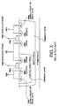
- a related semiconductor memory device such as, a flash memory or an EEPROM (Electrically Erasable Programmable ROM), includes a plurality of memory cells MC1 - MCn, row sub-decoders (namely, word line driving circuits) SD, and a plurality of row main decoders MD.
- a decoder MD is illustrated in Fig. 1 for convenience.
- each memory cell MC1 - MCn is electrically writable and erasable, and each row sub-decoder SD selects a row of each memory cell MC1 - MCn. Further, each row main decoder MD decodes a row address signal and supplies output signals XB, XB to the row sub-decodes SD.
- the row main decoder is composed of two stages of level shift circuits 15, 16 and the output signals XB and XB thereof are complementary to each other.
- a memory cell array is structured by a plurality of memory cells arranged in a matrix form.
- a plurality of word lines WL are connected to control gates of the respective memory cells arranged in the row direction while a plurality of bit lines BL are connected to drains of the respective memory cells arranged in the row direction.
- a plurality of word lines WL are divided into some blocks, and each block is selected by one of the row main decoders MD.
- the row sub-decoder SD for selecting the row of the memory cell MC1 is composed of one p-channel transistor P11 and two of n-channel transistors N11, N12.
- sources of the transistor P11 and the transistor N11 are connected to an XSPP node which is given a pre-decode signal (XSPP) while a source of the transistor N12 is coupled to a ground terminal (GND).
- XSPP pre-decode signal
- GND ground terminal
- Drains of the respective transistors P11, N11, N12 are connected to the word line (WL). Further, the output signal XB is given to gates of the transistor P11 and the transistor N12 while the output signal XB is given to a gate of the transistor N11.
- a back gate of the transistor P11 is coupled to a back gate voltage (PBG) node while back gates of the both transistors N11, N12 are connected to a back gate voltage (NBG) node, respectively.
- PBG back gate voltage
- NSG back gate voltage
- Each of the row sub-decoders for driving the other memory cells MC2 - MCn is structured by the respective transistors Pn1, Nn1, Nn2 in the same manner. These row sub-decoders are controlled by the pre-decode signals XSPP and the output signals XB, XB to determine potential of each word line (WN).
- a first level shift circuit 15 is composed of two pairs of transistors which are connected between a mode switching power supply (VPX) node and a ground node in series. More specifically, the level shift circuit 15 is composed of a p-channel transistor PM1 and an n-channel transistor NM1, and a p-channel transistor PN2 and an n-channel transistor NM2.
- an output of a NAND gate 13 is given to a gate of the transistor NM1 while an output of an inverter circuit 14 is given to a gate of the transistor NM2. Further, a series connection point between the transistor PM1 and the transistor NM1 is coupled to a gate of the transistor PM2 while a series connection point between the transistor PM2 and the transistor NM2 is coupled to a gate of the transistor PM1.
- the transistor PM1 is turned on, and the drain of the transistor PM1 and the gate of the transistor PM2 are put into VPX. At this time, the transistors NM1 and PM2 are turned off:
- the first level shift circuit 15 converts the binary signal of [0V, VDD] as the output of the NAND gate 13 into the binary signal [0V, VPX].
- a second level shift circuit 16 is composed of two pairs of transistors which are connected between a VPX node and a mode switching power supply voltage (VBB) in series. More specifically, the second level shift circuit 16 is composed of a transistor PM3 and a transistor NM3, and a transistor PM4 and a transistor NM4.
- the output is given to the gate of the transistor PM3 from a series connection point between the transistor PM2 and the transistor NM2. Further, the output is given to the gate of the transistor PM4 from a series connection point between the transistor PM1 and the transistor NM1.
- a series connection point between the transistor PM3 and the transistor NM3 is connected to the gate of the transistor NM4 while a series connection point between the transistor PM4 and the transistor NM4 is connected to the gate of the transistor NM3.
- the drain of the transistor NM2 is becomes 0V.
- the transistor PM4 is tuned on to put the output signal XB into VPX. Consequently, the gate of the transistor NM3 becomes VPX, and the transistor NM3 is turned on to put the output signal XB into VBB. At this time, the transistors NM4 and PM3 are turned off.
- the output of the NAND gate 13 is equal to VDD, the drain of the transistor NM1 becomes 0 V. Thereby, the transistor PM3 is turned on to put the output signal XB into VPX. In Consequence, the gate of the transistor NM4 becomes VPX. As a result, the transistor NM4 is turned on to put the output signal XB into VBB. At this time, the transistors NM3 and PM4 are turned off.
- the second level shift circuit 16 converts the binary signal of [0V, VPX] as the output of the first level shift circuit 15 into the binary signal of [VBB, VPX].
- the output signal XB is produced from the series connection point between the transistor PM3 and the transistor NM3 of the second level shift circuit 16 while the output signal XB is produced from the series connection point between the transistor PM4 and the transistor NM4.
- the output signals XB and XB are in the complementary relationship.
- each voltage of each terminal in each operation mode of the row decoder illustrated in Fig. 1 is represented in Fig. 2.
- the row main decoder MD illustrated in Fig. 1 is selected by the row address to select the word line WL1, and the word lines WL2 - WLn and the row main decoders (not shown) are not selected.
- the mode switching power supply voltage VPX and the node switching power supply voltage VBB of the low potential side, which are applied to the row main decoder MD, are 5V and -9 V, respectively, as illustrated in Fig. 2.
- the back gate voltage PBG of the p-channel transistor is equal to 0V while the back gate voltage NBG of the n-channel transistor is equal to -9 V.
- the output signal XB becomes a supply voltage 5V, and the output signal XB becomes -9 V. Further, the pre-decode signal XSPP1 is put into -9 V while XSPP2 - n become 0V. Consequently, the transistor N11, and P21 - Pn1 are turned on. As a result, the word line signal WL1 is put into -9 V while all of the word lines WL2 - WLn are put into 0V.
- the pre-decode signal XSPP1 of the memory block (not shown), which is not selected, becomes -9 V.
- the output signal XB becomes -9 V
- the output signal XB becomes the supply voltage 5V. Consequently, the transistors N12 - Nn2 are turned on, and all of the word line signals WL1 - WLn of non-selective blocks becomes 0V.
- the mode switching power supply voltage VPX and the back gate voltage PBG is equal to 1 V, respectively. Further, the mode switching power supply voltage VBB at the low potential side and the back gate voltage NBG is equal to 0 V, respectively.
- the respective pre-decode signals XSPP1 - n and the output signal XB are equal to 11 V, respectively while the output signal XB is equal to 0 V.
- the transistors P11 - Pn1 are turned on, and the word line signals WN1 - WLn are equal to 11V, respectively.
- the pre-decode signals XSPP1 - n of the non-selective memory blocks are equal to 11V.
- the output of the address decoder 13 becomes VDD.
- the output signal XB is put into 0V, and the output signal XB is put into 11V. Consequently, the transistors N12 - Nn2 are turned on, and all of the word line signals WL1 - WLn of the non-selective blocks becomes 0V.
- the mode switching power supply voltage VPX and the back gate voltage PBG become the power supply voltage, respectively. Further, the mode switching power supply voltage VBB at the lower potential side and the back gate voltage are equal to 0V, respectively.
- the output signal XB becomes the supply voltage VDD and the output signal XB becomes 0 V.
- the pre-decode signal XSPP1 is put into VDD while XSPP2 - n are equal to 0 V, respectively.
- the transistors P11, N21 - Nn1 are turned on.
- the word line signal WL1 is put into VDD while WL2 - n are equal to 0V, respectively.
- the pre-decode signal XSPP1 of the non-selective memory blocks becomes VDD.
- the output of the address decoder 13 becomes VDD and the output signal XB is equal to 0V.
- the output signal XB becomes the supply voltage VDD. Consequently, the transistors N12 - Nn2 are turned on, and the word line signals WL1- WLn of the non-selective blocks become 0V, respectively.
- the output signals XB , XB of the row main decoder MD for controlling the word line driving circuit SD becomes 5V at the high level and -9 V at the low level during the writing operation in the row decoder RD arranged for the flash memory.
- a high voltage of 5 - (-9) 14V is applied to a PN junction of the transistor constituting the level shift circuit MD.
- the back gate potential (NBG) of the transistor N12 constituting the word line driving circuit SD is put into -9V during the writing operation.
- the threshold voltage becomes, for example, about 3.5 V because of the back gate bias effect.
- the gate potential of the transistor N12 is selected to a higher value than 3.5 V to put the potential of the word line (WL) into 0 V by turning on the transistor N12.
- VDD is used as VPX, and VDD is set to about 5V.
- the supply power source VDD trends to become lower between 1.8 and 3.6V.
- the output voltage XB does not satisfy the threshold voltage of the transistor N12 Consequently, the transistor N12 is not turned on.
- a voltage of 14 V is applied between an N + region and a P-well of a high voltage (a high breakdown voltage) of the transistor, and between a P + region and a deep N-well. Consequently, it is necessary that the breakdown level of the PN junction is designed to (14+ ⁇ )V.
- the deep well prevents the current from flowing across the junction portion when a negative potential is applied to a P-substrate (GND).
- a row main decoder and a low sub-decoder are arranged in accordance with a plurality of cell-blocks.
- the low sub-decoder includes a PMOS transistor which is inserted and connected between an input node of the cell-block and a word line, and an NMOS transistor for pull-down which is connected to the word line and a ground node.
- the row main decoder produces a plurality of control signals of which potentials are restricted in accordance with during erasing selection/writing non-selection of the cell block and during erasing non-selection/writing selection, and supplies the respective control signals to the gate of the PMOS transistor and NMOS transistor of the row-sub decoder.
- This EEPROM prevents the large electric filed from being applied to the gate insulating film of the specific transistor in the row sub-decoder during writing and erasing. In consequence, reduction of reliability can be avoided.
- non-volatile semiconductor device is not applicable for the semiconductor memory device, such as, the flash memory.
- applied voltages to be applied to the memory cells during the writing operation are different from each other.
- a semiconductor memory device includes a plurality of memory cells, a row sub-decoder, a row main decoder and reducing means.
- the memory cells are arranged in a matrix form.
- the row sub-decoder selects each row of the memory cells. Further, the row main decoder decodes a row address signal and supplies a control signal into the row sub-decoder.
- the row main decoder is structured by at least one transistor having a PN junction breakdown voltage.
- the reducing means reduces the PN junction breakdown voltage during an erasing mode.
- each of the memory cells is electrically writable and erasable.
- a pre-decode signal is given to the row sub-decoder and is supplied to the memory cell via a word line.
- the reducing means sets a potential of the word line to a ground potential.
- the reducing means is placed in the row sub-decoder and is structured by at a transfer gate.
- the transfer gate is composed of at least one p-channel transistor.
- the row sub-decoder has a ground potential node.
- the p-channel transistor is connected between the word line and the ground potential node.
- the p-channel transistor has a source, a drain and a gate. In this condition, the source is connected to the ground potential node while the drain is connected to the word line.
- the control signal is given to the gate from the row main decoder.
- control signal has predetermined amplitude, and the predetermined amplitude falls within the range between a zero potential and a negative potential.
- the row main decoder is composed of at least one level shift circuit.
- the level shift circuit produces different voltages in accordance with each mode of a writing mode, an erasing mode and a reading mode as the control signal.
- the memory cell is a flash memory.
- a negative voltage is applied to the flash memory in the writing mode.
- the reducing means reduces the PN junction voltage of the transistor of the row main decoder in the writing mode.
- the breakdown level of the PN junction can be reduced.
- the row main decoder is composed of level shift circuits of a plurality of stages in which the mode switching signals are different to each other, and the output signals XB, XB becomes the binary signals [0V, -9 V].
- the voltage applied to the PN junction of the transistor constituting the level shift circuit is further reduced in the writing mode. Consequently, the breakdown level of the PN junction can be further reduced.
- a row decoder RD10 arranged in a semiconductor memory device such as, a flash memory or an EEPROM (Electrically Erasable Programmable ROM), includes a plurality of memory cells MC1 - MCn, row sub-decoders (namely, word line driving circuits) SD, and a plurality of row main decoders MD.
- a semiconductor memory device such as, a flash memory or an EEPROM (Electrically Erasable Programmable ROM)
- a row decoder RD10 includes a plurality of memory cells MC1 - MCn, row sub-decoders (namely, word line driving circuits) SD, and a plurality of row main decoders MD.
- a decoder MD is illustrated in Fig. 4 for convenience.
- each memory cell MC1 - MCn is electrically writable and erasable, and the each row sub-decoder SD selects a row of each memory cell MC1 - MCn. Further, each row main decoder MD decodes a row address signal and supplies output signals XB, XB to the row sub-decoders SD.
- the row main decoder is composed of level shift circuits 15, 16, and the output signals XB and XB thereof are complementary to each other.
- a memory cell array is structured by a plurality of memory cells arranged in a matrix form.
- a plurality of word lines WL are connected to control gates of the respective memory cells arranged in a row direction while a plurality of bit lines BL are connected to drains of the respective memory cells arranged in the row direction.
- a plurality of word lines WL are divided into some blocks, and each block is selected by one of the row main decoders MD.
- the row sub-decoder SD corresponding to the word line WL1 is composed of two p-channel transistors P11, P12 and two n-channel transistors N11, N12.
- sources of the transistor P11 and the transistor N11 are connected to an XSPP node which is given a pre-decode signal (XSPP) while sources of the transistor N12 and transistor P12 are coupled to a ground terminal (GND).
- XSPP pre-decode signal
- GND ground terminal
- Drains of the respective transistors P11, P12, N11, N12 are connected to the word line (WL). Further, the output signal XB is given to gates of the transistor P11 and the transistor N12 while the output signal XB is given to gates of the transistor N11 and the transistor P12.
- back gates of both the transistor P11, P12 are connected to a back gate voltage (PBG) node while back gates of the both transistors N11, N12 are connected to a back gate voltage (NBG) node, respectively.
- PBG back gate voltage
- NSG back gate voltage
- the p-channel transistor P12 serves as a transfer gate connected between the word line (WL) and the ground potential node.
- Each of the row sub-decoders for driving the other memory cells MC2 - MCn is structured by the respective transistors Pn1, Pn2, Nn1, Nn2 in the same manner. These row sub-decoders are controlled by the pre-decode signals XSPPn and the output signals XB, XB to determine potential of each of the word lines (WL).
- the row main decoder MD is composed of a NAND gate 13 which decodes a row address signal, an inverter circuit 14 which converts an output of the NAND gate 13, a first level shift circuit 15 which shifts a level of an output of the NAND gate 13, and a second level shift circuit 16 which shifts an output level of the first level shift circuit 15.
- a first level shift circuit 15 is composed of two pairs of transistors which are connected between a mode switching power supply (VPX) node and a ground node in series. More specifically, the level shift circuit 15 is composed of a p-channel transistor PM1 and an n-channel transistor NM1, and a p-channel transistor PN2 and an n-channel transistor NM2.
- an output of a NAND gate 13 is given to a gate of the transistor NM1 while an output of an inverter circuit 14 is given to a gate of the transistor NM2. Further, a series connection point between the transistor PM1 and the transistor NM1 is coupled to a gate of the transistor PM2 while a series connection point between the transistor PM2 and the transistor NM2 is coupled to a gate of the transistor PM1.
- the first level shift circuit 15 converts the binary signal of [0V, VDD] as the output of the NAND gate 13 into the binary signal [0V, VPX].
- a second level shift circuit 16 is composed of two pairs of transistors which are connected between a VPX node and a mode switching power supply voltage (VBB) at a low potential side in series. More specifically, the second level shift circuit 16 is composed of a transistor PM3 and a transistor NM3, and a transistor PM4 and a transistor NM4.
- the output is given to the gate of the transistor PM3 from a series connection point between the transistor PM2 and the transistor NM2. Further, the output is given to the gate of the transistor PM4 from a series connection point between the transistor PM1 and the transistor NM1.
- a series connection point between the transistor PM3 and the transistor MM3 is connected to the gate of the transistor NM4 while a series connection point between the transistor PM4 and the transistor NM4 is connected to the gate of the transistor NM3.
- the second level shift circuit 16 converts the binary signal of [0V, VPX] as the output of the first level shift circuit 15 into the binary signal of [VBB, VPX].
- the output signal XB is produced from the series connection point between the transistor PM3 and the transistor NM3 of the second level shift circuit 16 while the output signal XB is produced from the series connection point between the transistor PM4 and the transistor NM4. In this event, the output signals XB and XB are in the complementary relationship.
- each voltage of each terminal in each operation mode of the low decoder MD, SD illustrated in Fig. 4 is represented in Fig. 5.
- the row main decoder MD illustrated in Fig. 4 is selected by the row address to select the word line WL1, and the word lines WL2 - WLn and the row main decoders MD (not shown) are not selected.
- the mode switching power supply voltage VPX and the mode switching power supply voltage VBB of the low potential is equal to a supply voltage VDD and -9 V, respectively, as illustrated in Fig. 5.
- the back gate voltage PBG of the p-channel transistor is equal to 0V while the back gate voltage NBG of the n-channel transistor is equal to -9 V.
- the output signal XB is put into the supply voltage VDD, and the output signal XB is put into -9 V. Further, the pre-decode signal XSPP1 becomes -9 V while XSPP2 - n become 0V.
- the transistor N11, and P21 - Pn1 are turned on.
- the word line signal WL1 becomes -9 V while all of the word lines WL2 - WLn become 0V.
- the pre-decode signal XSP1 of the memory block (not shown), which is not selected, becomes -9 V.
- the output of the address decoder 13 becomes VDD
- the output signal XB becomes -9 V
- the output signal XB becomes the supply voltage VDD.
- the transistors P12 - Pn2 are turned on, and the word line signals WL1-WLn of non-selective blocks becomes 0V.
- VDD exceeds NBG (VDD > NBG)
- the transistors N12 - Nn2 are also turned on.
- the mode switching power supply voltage VPX and the back gate voltage PBG is equal to 1 V, respectively. Further, the mode switching power supply voltage VBB at the low potential side and the back gate voltage NBG is equal to 0 V, respectively.
- the respective pre-decode signals XSPP1 - n and the output signal XB are equal to 11 V, respectively while the output signal XB is equal to 0 V.
- the transistors P11 - Pn1 are turned on, and the word line signals WN1 - WLn are equal to 11V, respectively.
- the pre-decode signals XSPP1 - n of the non-selective memory blocks are equal to 11V.
- the output of the address decoder 13 becomes VDD.
- the output signal XB becomes 0V, and the output signal XB becomes 11V.
- the transistors N12 - Nn2 are turned on, and the word line signals WL1 - WLn of the non-selective blocks becomes 0V.
- the mode switching power supply voltage VPX and the back gate voltage PBG is equal to the power supply voltage VDD, respectively. Further, the mode switching power supply voltage VBB at the lower potential side and the back gate voltage NBG are equal to 0V, respectively.
- the pre-decode signal XSPP1 is put into VDD while XSPP2 - n are equal to 0 V, respectively.
- the transistors P11 - Pn1 are turned on.
- the word line signal WL1 becomes VDD while WL2 - n are equal to 0V, respectively.
- the pre-decode signal XSPP of the non-selective memory blocks becomes VDD.
- the output of the address decoder 13 becomes VDD and the output signal XB is equal to 0V. Further, the output signal XB is put into the supply voltage VDD.
- the transistors N12 - Nn2 are turned on, and the word line signals WL1 - WLn of the non-selective blocks become 0V, respectively.
- the output signals XB , XB of the row main decoder MD for controlling the word line driving circuit SD becomes the supply voltage VDD at the high level and -9 V at the low level during the writing operation.
- VDD - (-9) a voltage of VDD - (-9) is applied to a PN junction of the transistor constituting the low main decoder MD.
- the supply voltage falls within the range between 1.8 and 3.6 V, and is reduced with about 1.4 V in comparison with the conventional case.
- the p-channel transistor P12 is added in the row sub-decoder SD.
- the output signal XB is equal to - 9 V even when the output signal XB is equal to the supply voltage VDD and the n-channel transistor N12 is not turned on.
- the P-channel transistor P12 is turned on and the potential of the word line WL1 can be put into 0V (namely, ground potential).
- the transistor P12 is necessary in only the writing mode. Although the transistor N12 does not function in the writing mode, the transistor remains because it is necessary in the other modes.
- the applied voltage to be applied to the memory cell MC is negative like the semiconductor memory device, such as, the flash memory according to this invention, a voltage applied to the PN junction of the transistor constituting the row main decoder MD is reduced during the writing mode. Thereby, the breakdown level of the PN junction can be reduced.
- a row main decoder MD includes a third level shift circuit 21 in addition to a first level shift circuit 15 and a second level shift circuit 16 in a row decoder RD20.
- the third level shift circuit 21 shifts a level of an output of the second level shift circuit 16.
- a mode switching power supply voltage VPX2 of the third level shift circuit 21 is different from a mode switching power supply voltage VPX1 of the first and second level shift circuits 15 and 16.
- a mode switching power supply voltage VBB2 of a lower potential side of the third level shift circuit 21 is different from a mode switching power supply voltage VBB1 of a lower potential side of the second level shift circuit 16.
- the row decoder R20 is similar to the row decoder illustrated in Fig. 4 in the other structure, operation and effect.
- the first level shift circuit 15 converts the binary signal of [0V, VDD] as the output of the NAND gate 13 into the binary signal [0V, VPX].
- the second level shift circuit 16 converts the binary signal of [0V, VPX] as the output of the first level shift circuit 15 into the binary signal of [VBB1, VPX1].
- the third level shift circuit 21 is composed of two pairs of transistors which are connected between a mode switching power supply (VPX2) node and a mode switching power supply voltage VBB2 node of a low potential side in series. More specifically, the third level shift circuit 21 is composed of a p-channel transistor PM5 and an n-channel transistor NM5, and a p-channel transistor PN6 and an n-channel transistor NM6.
- An output is given to a gate of the transistor PM5 from a series connection point between the transistor PM4 and the transistor NM4 of the second level shift circuit 16.
- an output is given to a gate of the transistor PM6 from a series connection point between the transistor PM3 and the transistor NM3 of the second level shift circuit 16.
- a series connection point between the transistor PM5 and the transistor NM5 is coupled to the gate of the transistor NM6 while a series connection point between the transistor PM6 and the transistor NM6 is coupled to the gate of the transistor NM5.
- the third level shift circuit 16 converts the binary signal of [VBB1, VPX1] into the binary signal [VBB2, VPX2].
- the output signal XB is produced from the series connection point between the transistor PM5 and the transistor NM5 of the third level shift circuit 21 while the output signal XB is produced from the series connection point between the transistor PM6 and the transistor NM6.
- the output signals XB and XB are in the complementary relationship.
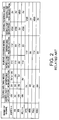
- each voltage of each terminal in each operation mode of the low decoder MD, SD illustrated in Fig. 6 is represented in Fig. 7.
- the row main decoder MD illustrated in Fig. 6 is selected by the row address to select the word line WL1, and the word lines WL2 - WLn and the row main decoders MD (not shown) are not selected.
- the mode switching power supply voltage VPX1 is equal to the power supply voltage VDD
- the mode switching power supply voltage VPX2 is equal to 0V
- the mode switching power supply voltage VBB1 of the low potential is equal to -4 V
- the mode switching power supply voltage VBB2 of the low potential is equal to -9V, respectively.
- the back gate voltage PBG of the p-channel transistor is equal to 0V while the back gate voltage NBG of the n-channel transistor is equal to -9 V.
- the output signal XB becomes the supply voltage 0V, and the output signal XB becomes -9 V. Further, the pre-decode signal XSPP1 becomes -9 V while XSPP2 - n become 0V.
- the transistor N11, and P21 - Pn1 are turned on.
- the word line signal WL1 becomes -9 V and the word lines WL2 - WLn becomes 0V.
- the pre-decode signal XSPP1 of the memory block (not shown), which is not selected, is put into -9 V.
- the output of the address decoder 13 is put into VDD, the output signal XB becomes -9 V, and the output signal XB becomes the supply voltage 0V.
- the transistors P12 - Pn2 are turned on, and the word line signals WL1 - WLn of non-selective blocks becomes 0V.
- the mode switching power supply voltage VPX1, VPX2 and the back gate voltage PBG are equal to 11 V, respectively. Further, the mode switching power supply voltage VBB1, VBB2 at the low potential side and the back gate voltage NBG are equal to 0 V, respectively.
- the respective pre-decode signals XSPP1 - n and the output signal XB are equal to 11 V, respectively while the output signal XB is equal to 0 V.
- the transistors P11 - Pn1 are turned on, and all of the word line signals WN1 - WLn are equal to 11V, respectively.
- the pre-decode signals XSPP1 - n of the non-selective memory blocks are equal to 11V.
- the output of the address decoder 13 becomes VDD.
- the output signal XB becomes 0V, and the output signal XB becomes 11V.
- the transistors N12 - Nn2 are turned on, and all of the word line signals WL1 - WLn of the non-selective blocks becomes 0V.
- the mode switching power supply voltage VPX1, VPX2 and the back gate voltage PBG are equal to the power supply voltage VDD, respectively. Further, the mode switching power supply voltage VBB1, VBB2 at the lower potential side and the back gate voltage NBG are equal to 0V, respectively.
- the output signal XB becomes the supply voltage VDD and the output signal XB becomes 0 V. Further, the pre-decode signal XSPP1 becomes VDD while XSPP2 - n are equal to 0 V, respectively.
- the transistors P11, N21 - Nn1 are turned on.
- the word line signal WL1 becomes VDD while WL2 - n are equal to 0V, respectively.
- the pre-decode signal XSPP1 of the non-selective memory blocks becomes VDD.
- the output of the address decoder 13 is put into VDD and the output signal XB is equal to 0V. Further, the output signal XB becomes the supply voltage VDD.
- the transistors N12 - Nn2 are turned on, and all of the word line signals WL1 - WLn of the non-selective blocks become 0V, respectively.
- the output signals XB, XB of the row main decoder MD for controlling the word line driving circuit SD becomes the supply voltage 0V at the high level and -9 V at the low level during the writing operation.
- the voltage applied to the PN junction of the transistor constituting the row main decoder MD is further reduced in the writing mode as compared to the first embodiment.
- the breakdown voltage of the PN junction can be further reduced.
- each of the n-channel transistor N12 and the p-channel transistor P12 is not limited to one, two or more may be arranged in the above-mentioned embodiments.
Landscapes
- Read Only Memory (AREA)
- Semiconductor Memories (AREA)
- Non-Volatile Memory (AREA)
Applications Claiming Priority (2)
| Application Number | Priority Date | Filing Date | Title |
|---|---|---|---|
| JP8134498 | 1998-03-27 | ||
| JP8134498A JP3223877B2 (ja) | 1998-03-27 | 1998-03-27 | 半導体記憶装置 |
Publications (2)
| Publication Number | Publication Date |
|---|---|
| EP0945873A2 true EP0945873A2 (fr) | 1999-09-29 |
| EP0945873A3 EP0945873A3 (fr) | 2000-07-05 |
Family
ID=13743760
Family Applications (1)
| Application Number | Title | Priority Date | Filing Date |
|---|---|---|---|
| EP99105106A Withdrawn EP0945873A3 (fr) | 1998-03-27 | 1999-03-25 | Dispositif de mémoire à semi-conducteurs |
Country Status (5)
| Country | Link |
|---|---|
| US (1) | US6128230A (fr) |
| EP (1) | EP0945873A3 (fr) |
| JP (1) | JP3223877B2 (fr) |
| KR (1) | KR100327857B1 (fr) |
| CN (1) | CN1230751A (fr) |
Families Citing this family (14)
| Publication number | Priority date | Publication date | Assignee | Title |
|---|---|---|---|---|
| KR100301932B1 (ko) * | 1999-04-27 | 2001-10-29 | 윤종용 | 불 휘발성 반도체 메모리 장치 |
| KR100338772B1 (ko) * | 2000-03-10 | 2002-05-31 | 윤종용 | 바이어스 라인이 분리된 비휘발성 메모리 장치의 워드라인 드라이버 및 워드 라인 드라이빙 방법 |
| US6396743B1 (en) * | 2001-05-18 | 2002-05-28 | Silicon Storage Technology, Inc. | Control circuit for a non-volatile memory array for controlling the ramp rate of high voltage applied to the memory cells and to limit the current drawn therefrom |
| KR100560653B1 (ko) * | 2003-02-10 | 2006-03-16 | 삼성전자주식회사 | 듀얼 절연막 체계를 갖는 반도체 집적 회로 장치 |
| KR100541687B1 (ko) * | 2004-06-23 | 2006-01-12 | 주식회사 하이닉스반도체 | 누설전류 감소를 위한 메모리 장치 |
| DE102005055834A1 (de) * | 2005-11-23 | 2007-05-24 | Infineon Technologies Ag | Speicherschaltung, Ansteuerschaltung für einen Speicher und Verfahren zum Einschreiben von Schreibdaten in einen Speicher |
| KR101202429B1 (ko) * | 2007-10-11 | 2012-11-16 | 삼성전자주식회사 | 저항체를 이용한 비휘발성 메모리 장치 |
| US7652947B2 (en) * | 2008-02-28 | 2010-01-26 | International Business Machines Corporation | Back-gate decode personalization |
| JP5537099B2 (ja) * | 2009-09-08 | 2014-07-02 | ルネサスエレクトロニクス株式会社 | 半導体装置 |
| JP5507288B2 (ja) * | 2010-02-24 | 2014-05-28 | ラピスセミコンダクタ株式会社 | 半導体記憶装置のデコーダ回路 |
| KR101787758B1 (ko) * | 2011-06-09 | 2017-10-19 | 매그나칩 반도체 유한회사 | 레벨 쉬프터 |
| KR102115639B1 (ko) * | 2016-07-27 | 2020-05-27 | 매그나칩 반도체 유한회사 | 전원 스위치 회로 |
| JP7065637B2 (ja) * | 2018-02-22 | 2022-05-12 | ルネサスエレクトロニクス株式会社 | 半導体装置 |
| TWI722830B (zh) * | 2020-03-13 | 2021-03-21 | 聯陽半導體股份有限公司 | 提供高驅動電壓的閘極驅動電路 |
Family Cites Families (5)
| Publication number | Priority date | Publication date | Assignee | Title |
|---|---|---|---|---|
| US4769787A (en) * | 1985-07-26 | 1988-09-06 | Hitachi, Ltd. | Semiconductor memory device |
| US5253200A (en) * | 1987-12-15 | 1993-10-12 | Sony Corporation | Electrically erasable and programmable read only memory using stacked-gate cell |
| JP2835215B2 (ja) * | 1991-07-25 | 1998-12-14 | 株式会社東芝 | 不揮発性半導体記憶装置 |
| JP3199882B2 (ja) * | 1993-01-13 | 2001-08-20 | 株式会社東芝 | 不揮発性半導体記憶装置 |
| JP2964982B2 (ja) * | 1997-04-01 | 1999-10-18 | 日本電気株式会社 | 不揮発性半導体記憶装置 |
-
1998
- 1998-03-27 JP JP8134498A patent/JP3223877B2/ja not_active Expired - Fee Related
-
1999
- 1999-03-25 EP EP99105106A patent/EP0945873A3/fr not_active Withdrawn
- 1999-03-26 KR KR1019990010439A patent/KR100327857B1/ko not_active Expired - Fee Related
- 1999-03-29 US US09/280,666 patent/US6128230A/en not_active Expired - Fee Related
- 1999-03-29 CN CN99103230A patent/CN1230751A/zh active Pending
Also Published As
| Publication number | Publication date |
|---|---|
| JP3223877B2 (ja) | 2001-10-29 |
| KR100327857B1 (ko) | 2002-03-09 |
| EP0945873A3 (fr) | 2000-07-05 |
| US6128230A (en) | 2000-10-03 |
| CN1230751A (zh) | 1999-10-06 |
| JPH11283390A (ja) | 1999-10-15 |
| KR19990078289A (ko) | 1999-10-25 |
Similar Documents
| Publication | Publication Date | Title |
|---|---|---|
| EP0090116B1 (fr) | Dispositif semi-conducteur CMOS comportant deux sources d'alimentation | |
| US5594687A (en) | Completely complementary MOS memory cell with tunneling through the NMOS and PMOS transistors during program and erase | |
| US20090122622A1 (en) | Level shifter with reduced leakage current and block driver for nonvolatile semiconductor memory device | |
| US5157281A (en) | Level-shifter circuit for integrated circuits | |
| US10734088B2 (en) | CMOS anti-fuse cell | |
| KR0155078B1 (ko) | 강전계용의 mos 회로를 갖춘 반도체 회로 | |
| US6128230A (en) | Semiconductor memory with PN junction potential reduction in a writing mode | |
| EP0658904A2 (fr) | Dispositif de circuit intégré à semi-conducteur | |
| EP1223619B1 (fr) | Procédé de fabrication d'un dispositif à semiconducteur | |
| CN113963738A (zh) | 反熔丝装置及反熔丝单元的编程方法 | |
| US7605633B2 (en) | Level shift circuit which improved the blake down voltage | |
| US6240014B1 (en) | Semiconductor memory device | |
| KR100233224B1 (ko) | 고전압 검출기 회로 | |
| KR100767136B1 (ko) | 불휘발성 반도체 기억 장치 | |
| EP0833343A2 (fr) | Porte NON/OU couplée à un sous-décodeur d'une mémoire à semi-conducteurs | |
| US5691944A (en) | Non-volatile semiconductor memory device | |
| EP0942432B1 (fr) | Dispositif de stockage non volatile à semi-conducteurs | |
| US6049498A (en) | Double transistor switch for supplying multiple voltages to flash memory wordlines | |
| US6292391B1 (en) | Isolation circuit and method for controlling discharge of high-voltage in a flash EEPROM | |
| KR20010092074A (ko) | 고전압 워드 라인 드라이버 회로를 구비한 반도체 메모리장치 | |
| CN110648697B (zh) | 选择电路、用于存储器存储系统的防闩锁电路及方法 | |
| US7279932B2 (en) | Semiconductor integrated circuit device | |
| US6570811B1 (en) | Writing operation control circuit and semiconductor memory using the same | |
| US7260014B1 (en) | Voltage supply circuit for memory array programming | |
| JPH09326686A (ja) | レベルシフト回路 |
Legal Events
| Date | Code | Title | Description |
|---|---|---|---|
| PUAI | Public reference made under article 153(3) epc to a published international application that has entered the european phase |
Free format text: ORIGINAL CODE: 0009012 |
|
| AK | Designated contracting states |
Kind code of ref document: A2 Designated state(s): DE FR GB |
|
| AX | Request for extension of the european patent |
Free format text: AL;LT;LV;MK;RO;SI |
|
| PUAL | Search report despatched |
Free format text: ORIGINAL CODE: 0009013 |
|
| AK | Designated contracting states |
Kind code of ref document: A3 Designated state(s): AT BE CH CY DE DK ES FI FR GB GR IE IT LI LU MC NL PT SE |
|
| AX | Request for extension of the european patent |
Free format text: AL;LT;LV;MK;RO;SI |
|
| RIC1 | Information provided on ipc code assigned before grant |
Free format text: 7G 11C 16/08 A, 7G 11C 8/00 B |
|
| 17P | Request for examination filed |
Effective date: 20000525 |
|
| AKX | Designation fees paid |
Free format text: DE FR GB |
|
| STAA | Information on the status of an ep patent application or granted ep patent |
Free format text: STATUS: THE APPLICATION HAS BEEN WITHDRAWN |
|
| 18W | Application withdrawn |
Effective date: 20021220 |