EP0945888A2 - Plasma-Anzeigevorrichtung - Google Patents
Plasma-Anzeigevorrichtung Download PDFInfo
- Publication number
- EP0945888A2 EP0945888A2 EP98309610A EP98309610A EP0945888A2 EP 0945888 A2 EP0945888 A2 EP 0945888A2 EP 98309610 A EP98309610 A EP 98309610A EP 98309610 A EP98309610 A EP 98309610A EP 0945888 A2 EP0945888 A2 EP 0945888A2
- Authority
- EP
- European Patent Office
- Prior art keywords
- plasma display
- main frame
- pdp
- display device
- conducting plate
- Prior art date
- Legal status (The legal status is an assumption and is not a legal conclusion. Google has not performed a legal analysis and makes no representation as to the accuracy of the status listed.)
- Granted
Links
Images




Classifications
-
- H—ELECTRICITY
- H05—ELECTRIC TECHNIQUES NOT OTHERWISE PROVIDED FOR
- H05K—PRINTED CIRCUITS; CASINGS OR CONSTRUCTIONAL DETAILS OF ELECTRIC APPARATUS; MANUFACTURE OF ASSEMBLAGES OF ELECTRICAL COMPONENTS
- H05K7/00—Constructional details common to different types of electric apparatus
- H05K7/20—Modifications to facilitate cooling, ventilating, or heating
- H05K7/20954—Modifications to facilitate cooling, ventilating, or heating for display panels
- H05K7/20963—Heat transfer by conduction from internal heat source to heat radiating structure
-
- H—ELECTRICITY
- H01—ELECTRIC ELEMENTS
- H01J—ELECTRIC DISCHARGE TUBES OR DISCHARGE LAMPS
- H01J2217/00—Gas-filled discharge tubes
- H01J2217/38—Cold-cathode tubes
- H01J2217/49—Display panels, e.g. not making use of alternating current
- H01J2217/492—Details
Definitions
- the present invention relates to a plasma display device using a plasma display panel (referred to as PDP, below). More particularly, it relates to a plasma display device having a new structure for supporting a PDP and for connecting a PDP with various driving circuits.
- PDP plasma display panel
- the AC type of plasma display device is comprised of a PDP and a main frame for supporting and holding circuit boards thereon.
- Various circuit components including circuits for driving the PDP are held on the circuit boards.
- the PDP is mainly comprised of two glass plates arranged in parallel with each other so as to hold a plasma forming gas therebetween, the main frame having circuit boards thereon and the PDP are stuck together using a binding material.
- the main frame should be designed by taking in account the possibility that it will be discarded. For this reason, a previously-considered main frame has been made in a simple form to reduce the manufacturing cost.
- the main frame has other functions, such as to quickly and uniformly absorb the heat generated by the PDP so that the entire PDP surface is maintained at a uniform temperature, thus keeping the display quality of the PDP high, and to quickly move the absorbed heat to the outside of the device through heat conduction and radiation.
- the main frame should be made from a material having a large thermal conductivity and should have a large surface area.
- the main frame cannot have a complicated and high cost structure to increase the thermal conductivity and the surface area. Accordingly, the previously-considered main frame has been made of a relatively thin metal plate.
- the main frame should have a high mechanical strength to protect the PDP from external stress since it is made of glass plates.
- the metal plate must be made thicker to ensure the mechanical strength of the main frame and the PDP. In this case, however, a problem arises in keeping the panel flat. This is because the panel is easily broken due to stress arising from an uneven panel.
- a plasma display device having a PDP, a circuit board having a driving circuit for driving the PDP, a main frame for supporting the circuit board, and a uniform heat-conducting plate to be supported by said main frame and, at the same time, to be fixed to said PDP.
- the main frame and the uniform heat-conducting plate which are detachably attached to each other, are desirably provided between the circuit board and the PDP. Therefore, various structures for solving the above-mentioned problems can be provided on the main frame which is easily separated from the uniform heat-conducting plate when the PDP is replaced.
- the uniform heat-conducting plate which is fixed to the PDP and can be discarded along with the PDP, can be formed in a simple form so as to reduce the manufacturing cost thereof. If the PDP must be replaced for some reasons after it has been incorporated into a plasma display device, only the PDP and the uniform heat-conducting plate fixed to the PDP must be discarded since the main frame is easily separated from the uniform heat-conducting plate.
- the uniform heat-conducting plate is desirably stuck to the PDP using a binding material.
- the binding material fixes the PDP and the uniform heat-conducting plate closely, and improves the heat conduction between the PDP and the uniform heat-conducting plate.
- the heat generated by the PDP can be conducted to the uniform heat-conducting plate quickly and uniformly, and, further, conducted efficiently to the main frame via the uniform heat-conducting plate.
- the uniform heat-conducting plate preferably comprises a plurality of convex and concave parts, which convex parts closely approach to the PDP and which concave parts hold a binding material to stick the uniform heat-conducting plate to the PDP.
- the mechanical strength of the uniform heat-conducting plate itself is increased due to the existence of the convex and concave parts and, at the same time, the required amount of the binding material can be reduced, thus realizing a low cost plasma display device. Since the uniform heat-conducting plate is structured to closely approach the PDP in the regions where no binding material exists, the heat conduction from the entire PDP surface to the uniform heat-conducting plate is kept excellent. Thus, the heat generated by the PDP is quickly and uniformly conducted to the uniform heat-generating plate and then to the main frame through the uniform heat-conducting plate.
- the uniform heat-conducting plate preferably has a plurality of spacers on one surface to closely approach the PDP, and a binding material is placed between the respective spacers so as to fix the uniform heat-conducting plate to the PDP.
- the advantages obtained by the third preferred embodiment of the present invention mentioned above can also easily be obtained.
- the spacers can perform at least one of the same functions as the convex parts of the third embodiment.
- the uniform heat-conducting plate having the spacers according to this embodiment may not have that remarkable advantage of increasing the mechanical strength of the plate, it can be made more easily than that having the convex and concave parts because no processing is necessary for the plate.
- the same advantages as those obtained by the third embodiment can be obtained by the fourth embodiment with respect to heat conduction and uniform heat-conduction.
- the main frame desirably has a plurality of tabs while the uniform heat-conducting plate has a plurality of sockets in which the corresponding tabs are inserted to detachably fix the main frame to the uniform heat-conducting plate.
- the tabs and the sockets are screwed together after the tabs have been inserted into the corresponding sockets.
- the main frame and the uniform heat-conducting plate can easily be fixed together and detached from each other.
- the main frame preferably has a heat radiating portion for efficiently dissipating the heat generated by the PDP to the outside of the device through heat radiation and heat conduction.
- the heat radiating portion may include a radiating fin.
- the heat generated by the PDP is efficiently dissipated from the radiating portion such as, for example, the radiating fin. Because these means for dissipating heat are formed to the main frame which is detachably attached to the uniform heat-conducting plate fixed to the PDP, the cost of a plasma display device according to this embodiment does not increase even though the device is produced assuming the possibility of discarding the PDP and the plate.
- the main frame desirably comprises a first rib formed along the outer periphery of the frame.
- the mechanical strength of the main frame can be increased by the first rib formed along the outer periphery of the frame and, at the same time, the thickness of the main frame can be reduced in the part where no first rib is formed, thus decreasing the total weight of the plasma display device.
- the surface area of the main frame increases as a result of the first rib formation, and therefore, the first rib acts as a radiation part.
- the main frame desirably has a through hole penetrating between the front and the back surfaces of the main frame.
- the main frame can be made to have less weight than a main frame having no through hole.
- the main frame preferably further comprises a second rib formed along the periphery of the through hole.
- the second rib formed along the periphery of the through hole can prevent a decrease in the mechanical strength of the main frame due to the formation of a through hole.
- the second rib increases the surface area of the main frame, it acts as a heat radiating portion.
- an embodiment of the present invention can provide a plasma display device having a new structure for coupling a PDP to a main frame so as to solve the various problems arising from the previously-considered coupling structure without largely increasing the manufacturing cost.
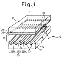
- Fig. 1 is an oblique view for showing the internal structure of the AC type color PDP.
- This type of color PDP is comprised of, for example, an AC type surface discharge panel having three electrodes.
- it is comprised of a front transparent substrate 21 made of glass and a back substrate 22 made of glass or ceramic.
- a plurality of address electrodes 23 arranged in parallel to each other with predetermined separations, a plurality of belt-shaped ribs 24 disposed between two adjacent address electrodes 23, and a luminescent layer 25, are formed as shown in Fig. 1.
- This luminescent layer 25 covers the address electrodes 23, and also covers the respective side surfaces of the ribs 24 as well.
- Luminescent layer 25 is comprised of a series of three different luminescent parts, for example, red luminescent parts 25R, green luminescent parts 25G and blue luminescent parts 25B, each of which emits a respective color of light under illumination by ultraviolet rays. These parts 25R, 25G and 25B are disposed among ribs 24 in a predetermined order.
- a plurality of display electrodes (sustaining electrodes) 26 made from a transparent conductive material are formed in the direction to intersect the address electrodes 23. These display electrodes 26 are disposed in parallel with each other, and each display electrode forms an electrode pair with an adjacent address electrode 23.
- a metal bus electrode 27 is formed to increase the conductivity of the display electrodes.
- a dielectric layer 28 is formed to cover the display electrodes 26 and the bus electrodes 27.
- ITO indium tin oxide
- SnO 2 tin oxide
- the metal bus electrodes 27 are made of, for example, a three layer electrode of Cr-Cu-Cr.
- the dielectric layer 28 is covered by a protection layer 29 made from magnesium oxide (MgO).
- the front transparent substrate 21 and the back substrate 22 are so disposed that a gap 30 is formed between the protection layer 29 and the luminescent layer 25.
- This gap 30 is made air-tight to enclose a low pressure gas inside.
- This gas is comprised of a gas material which emits ultraviolet rays when activated to become a plasma.
- a gas made of two gas components such as neon and xenon or helium and xenon, or three gas components such as helium, argon and xenon or neon, argon and xenon may be used as the plasma gas material. Using these gas materials, a PDP having a long life, a low operational voltage and a high brightness may be obtained.
- Fig. 2 is an exploded view, in an oblique direction, of a previously-considered plasma display device which incorporates the PDP shown in Fig. 1.
- reference numeral 10 denotes the PDP shown in Fig. 1
- 4 denotes a tip tube used to exhaust the air inside the PDP
- 17a denotes a main frame
- 11 and 12 denote circuit boards having driving circuits etc.
- 13 denotes a driver.
- PDP 10 is basically made of a pair of glass plates, and therefore, the circuit boards 11 and 12 cannot be directly fixed to PDP 10 with screws.
- the circuit boards 11 and 12 are fixed to the main frame 17a made of, for example, a metal plate, and thereafter, the main frame 17a is stuck to PDP 10 with, for example, a double coated adhesive tape.
- Reference numerals 14 and 15 denote covers for protecting the respective circuit boards 11 and 12, and 16 denotes a driver cover for protecting the driver 13, which driver cover also functions to be a heat sink for the driver 13.
- main frame 17a which contacts the PDP 10, is required to absorb the heat generated by PDP 10 quickly and uniformly and move it quickly to the outside of the device.
- frame 17a should be made from a material having a large thermal conductivity as well as having a large surface area.
- a possibility to abandon the frame 17a along with the PDP 10 must be taken in account as mentioned above, a complicated and high cost structure to improve the heat absorption and heat discharge cannot be used for the main frame 17a.
- Fig. 3 is a cross-sectional view showing an example structure to improve the uniform heat-conduction between the PDP 10 and the main frame 17a.
- Fig. 3 is an enlarged view of the circled part shown in Fig. 2.
- the frame 17a is stuck to PDP 10 by means of strips of adhesive 1 made of, for example, double coated adhesive tape.
- the strips of adhesive 1 are arranged at almost equal distances between the frame 17a and PDP 10.
- strips of heat-conductive rubber sheet 2 are disposed between strips 1. Since strips of heat-conductive rubber sheet 2 have a high thermal conductivity, they are expected to quickly absorb the heat generated by the PDP 10 and conduct it to the main frame 17a, thus realizing the uniform heat-conduction between the PDP 10 and the main frame 17a. However, this structure does not improve the heat discharge efficiency of the main frame 17a.
- the previously-considered plasma display device usually obtains its mechanical strength from an external framework member to which the plasma display device is installed.
- Various external framework members are used depending on apparatuses in which the plasma display device is installed.
- frame 17a and the external framework member are engaged together with, for example, screws via circuit boards 11 and 12 and covers 14 and 15.
- the previously-considered plasma display device since many through holes for the screws cannot be provided on the circuit boards, the previously-considered plasma display device has only a few engaging portions. As a result, the PDP of the conventional plasma display device may easily warp or twist due to an unbalanced load distribution caused by the engaging portions when the device receives an impact from the outside of the device. Therefore, the lack of stiffness has been a serious problem in the previously-considered plasma display device.
- the main frame 17a is made thick. However, if frame 17a is thickened, it is difficult to maintain the flatness of the main frame 17a. When the main frame 17a is made thin, PDP 10 does not receive a large load even though the flatness of the main frame 17a is low, that is, little warp exists. This does not result in a serious problem. On the contrary, when the main frame is made thick and the panel 10 is stuck to the warped frame 17a, it receives a large load. This results in breakage of the panel.
- a plasma display device embodying the present invention has a new frame structure which is able to solve the above-mentioned various problems without largely increasing the manufacturing cost of the plasma display device.
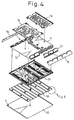
- Fig. 4 is an exploded view in an oblique direction of a plasma display device according to a first embodiment of the present invention.
- the same reference numerals in Fig. 4 as those of in Figs. 2 and 3 show the same or similar structure elements, and therefore, a detailed explanation of these structural elements will not be given.
- FIG. 4 17 denotes a main frame and 18 a uniform heat-conducting plate. Plate 18 is supported by main frame 17 and, at the same time, fixed to PDP 10 by an adhesive. On main frame 17, circuit boards 11 and 12 having, for example, driving circuits, are mounted.
- Reference numeral 13 denotes a driver provided on the edges of circuit boards 11 and 12. This driver 13 is connected to PDP 10 via a cable (not shown) to drive the respective electrodes formed in PDP 10.
- Reference numerals 14 and 15 denote protect covers provided to cover the respective circuit boards 11 or 12.
- Reference numeral 16 denotes a driver cover to protect driver 13. At the same time, it functions as a heat discharge plate to move the heat generated by driver 13 to the outside of the driver.
- Reference numeral 4 denotes a tip tube for evacuating gas from the inside of PDP 10. A notch is provided on the corresponding portion of plate 18 so that plate 18 does not contact with the tip tube 4 when plate 18 is stuck to PDP 10.
- the main frame 17a could not have a complicated structure which invites an increase of the manufacturing cost.
- the main frame 18 of a device embodying the present invention may have a complicated structure which can improve its heat discharge ability and mechanical strength by providing the uniform heat-conducting plate 18 between the PDP 10 and the main frame 17.
- Figs. 5A to 5C are cross sectional views showing a part of the structure of respective plates 18 according to first to third embodiments of the present invention. These figures show the enlarged structures of the circled part shown in Fig. 4.
- Fig. 5A shows the simplest structure in which a rolled aluminum plate 18a is stuck to PDP 10 with an adhesive 1a. Although a uniform layer of adhesive 1a is provided in the structure shown in Fig. 5A, in a device embodying the present invention it may be possible to place a double coated adhesive tape between the plate 18a and PDP 10.
- FIG. 5B shows another example of a plate in which adhesive layers are partly formed between the plate 18b and PDP 10.
- plate 18b is comprised of a plurality of stripe-like convex parts 181 and concave parts 182 which are alternately and periodically formed on the plate 18b. This plate 18b contacts with PDP 10 through the convex parts 181.
- adhesive layers 1b are formed between the plate 18b and PDP 10 so as to stick them together.
- the adhesive material must have an excellent thermal resistance and thermal conduction, and therefore, a double coated adhesive tape, "VHBTM Acrylic Form Structural Adhesive Tape" made by 3M Co. might be used in this embodiment.
- a double coated adhesive tape "VHBTM Acrylic Form Structural Adhesive Tape" made by 3M Co.
- the double coated adhesive tape is periodically placed so that the tape cost is reduced as compared with the case where the adhesive tape is placed on the entire surface of PDP 10 as shown in Fig. 5A.
- the convex parts 181 where no adhesive tape is placed may be processed to contact with PDP 10 so as not to form a gap between plate 18b and PDP 10.
- the convex parts 181 is expected to completely contact with PDP 10, however, a small gap depending on the processing accuracy may exist.
- Plate 18b may be realized by processing a rolled aluminum plate in a drawing or a press working.
- the periodically formed convex and concave parts improve the mechanical strength of the plate 18b.
- the embodiment shown in Fig. 4 uses plate 18b as the uniform heat-conducting plate 18. From this figure, it is clearly understood that a plurality of convex and concave parts are formed in a stripe form.
- the present embodiment forms the convex and concave parts in a stripe form periodically, these parts need not always be formed in a stripe form. For example, they may be formed in a lattice form or even more randomly. The form may be changed freely depending on design requirements.
- Fig. 5C shows still another example of the uniform heat-conducting plate 18.
- Reference numeral 18c denotes the uniform heat-conducting plate of this example, the plate 18c which has the same effect as that of the plate 18b shown in Fig. 5A without conducting the drawing or the press working mentioned above.
- spacers 3 are disposed in places corresponding to the convex parts 181 of the plate 18b, that is, between the adhesives 1c.
- this example can easily realize a low cost plate because the above mentioned drawing or the press working method is no longer necessary.
- spacers 3 are not limited to the stripe form shown, but any form including square and lattice forms may be applicable.
- the heat generated by the PDP 10 is uniformly conducted to the respective plate 18a, 18b or 18c so that no hot spot is formed on the plate 18. Then the heat is quickly discharged to the outside of the device through the main frame 17 which is attached to the plate 18a, 18b or 18c.
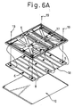
- Fig. 6A is an exploded view, in an oblique direction, of the structure for coupling the main frame and the uniform heat-conducting plate.
- the uniform heat-conducting plate 18 may be discarded with PDP 10, and therefore, it cannot have a complicated structure which may increase the cost.
- the embodiment shown in Fig. 4 forms the "complicated structure" on the main frame 17, which support the relatively low cost plate 18, so as to realize the above mentioned various functions.
- the main frame 17 of this embodiment has a plurality of tabs 5 (for example, 11, in Fig. 3) which combines main frame 17 with the plate 18.
- a plurality of sockets 6 are formed on the plate 18 so as to receive the respective tabs 5 formed on the main frame 17.
- Fig. 6B is a view showing the detailed structure how the tab 5 is received by the socket 6 to engage the main frame 17 to the plate 18.
- the main frame 17 is first superposed to the plate 18 in such a way that the corresponding tabs 5 and sockets 6 face to each other. Then, either one of main frame 17 or plate 18 is slid so as to push the tabs 5 into corresponding sockets 6. In this condition, a screw 19 is inserted into the respective screw hole 7 to fix the tab to the socket. As a result, main frame 17 is secured and fixed to plate 18.
- main frame 17 is disposed between PDP 10 and circuit boards 11 and 12, and works as a rigid body to improve the mechanical strength of PDP 10. Accordingly, in this embodiment, plate 18, which has been stuck to PDP 10, can easily be fixed to the main frame 17, which is a rigid body, through a plurality of engaging portions, thus improving the mechanical strength of the PDP 10. Due to this improvement in mechanical strength, a plasma display device embodying this invention can uniformly distribute the load caused by an external impact, thus preventing PDP 10 from being bent. Since recent PDPs have a tendency to be made more and more precise, electrodes and rib structures within the panel must be made very fine and precise. Therefore, the unbent structure of the panel is very effective to maintain the high reliability of a plasma display device.
- Fig. 7A is an oblique view showing the structure after the main frame 17 has been fixed to PDP 10 through plate 18.
- Fig. 7B shows the enlarged structure of the circled part shown in Fig. 7A.
- reference numeral 31 denotes the secured part where a tab 5 is inserted into a socket 6 and fixed each other by a screw 19.
- the total of eleven secured parts 31 are provided on the frame structure such that four of them are on the respective corners, four are on each center of four edges and the remaining three are disposed at equal distances between the secured parts provided on each center of the short edges.
- Rib 32 is formed along the edges of main frame 17 so as to increase the strength of the main frame 17. Due to the rib 32, main frame 17 can be made as thin as possible except the rib part, thus reducing the weight of the main frame 17 without reducing its mechanical strength. Through holes 35 are formed to penetrate the main frame 17, thus further reducing the weight of the main frame 17. Ribs 33 are formed to the main frame 17 along the respective peripheries of the through holes 35 so as to compensate for the decrease in mechanical strength of the main frame 17 due to the formation of the through holes 35.
- Radiating fin 34 is provided to effectively move the heat generated by PDP 10 from the main frame 17 to the outside of the device through heat radiation and heat conduction.
- eight fins are provided on the main frame 17.
- the above mentioned ribs 32 and 33 also work as heat dissipating parts.
- the main frame 17 can have the above mentioned complicated structure having ribs and fins because the uniform heat-conducting plate 18, which may be discarded is provided separately in addition to the main frame.
- main frame 17 can easily be separated from the uniform heat-conducting plate 18, only PDP 10 and the low cost plate 18 must be replaced.
- the main frame 17 having the above mentioned structure can be manufactured by a precut method from an aluminum plate. However, for mass production, an aluminum die casting is preferable.
- a plasma display device embodying the present invention is provided with a uniform heat-conducting plate fixed to the plasma display panel and a main frame supported by the uniform heat-conducting plate. Accordingly, a plasma display device embodying this invention can solve the various problems arriving from the structure for coupling a plasma display panel with a main frame having circuit boards, such as problems concerning the heat dissipation and the mechanical strength of the panel, without largely increasing the manufacturing cost of the plasma display panel.
Landscapes
- Physics & Mathematics (AREA)
- Thermal Sciences (AREA)
- Engineering & Computer Science (AREA)
- Microelectronics & Electronic Packaging (AREA)
- Devices For Indicating Variable Information By Combining Individual Elements (AREA)
- Gas-Filled Discharge Tubes (AREA)
Applications Claiming Priority (2)
| Application Number | Priority Date | Filing Date | Title |
|---|---|---|---|
| JP07750698A JP3747306B2 (ja) | 1998-03-25 | 1998-03-25 | プラズマディスプレイ装置 |
| JP7750698 | 1998-03-25 |
Publications (3)
| Publication Number | Publication Date |
|---|---|
| EP0945888A2 true EP0945888A2 (de) | 1999-09-29 |
| EP0945888A3 EP0945888A3 (de) | 2000-01-12 |
| EP0945888B1 EP0945888B1 (de) | 2004-07-14 |
Family
ID=13635863
Family Applications (1)
| Application Number | Title | Priority Date | Filing Date |
|---|---|---|---|
| EP98309610A Expired - Lifetime EP0945888B1 (de) | 1998-03-25 | 1998-11-24 | Plasma-Anzeigevorrichtung |
Country Status (6)
| Country | Link |
|---|---|
| US (1) | US6288489B1 (de) |
| EP (1) | EP0945888B1 (de) |
| JP (1) | JP3747306B2 (de) |
| KR (1) | KR100309964B1 (de) |
| DE (1) | DE69825030T2 (de) |
| TW (1) | TW428153B (de) |
Cited By (4)
| Publication number | Priority date | Publication date | Assignee | Title |
|---|---|---|---|---|
| US6617767B2 (en) | 2000-10-16 | 2003-09-09 | Lg Electronics Inc. | Thermal dispersing system of a plasma display device |
| US7245076B2 (en) | 2001-04-24 | 2007-07-17 | Fujitsu Hitachi Plasma Display Limited | Plasma display apparatus with main frame and adhesives having holes |
| EP1357574A3 (de) * | 2002-04-26 | 2008-11-19 | Panasonic Corporation | Herstellungsverfahren und Verfahren zum Abbau einer Plasma-Anzeigevorrichtung |
| EP1835376A3 (de) * | 2006-03-17 | 2010-10-06 | Hitachi, Ltd. | Flachbildschirm |
Families Citing this family (69)
| Publication number | Priority date | Publication date | Assignee | Title |
|---|---|---|---|---|
| US6737790B2 (en) * | 1998-05-19 | 2004-05-18 | Canon Kabushiki Kaisha | Image forming apparatus having a heat insulating member |
| TW472944U (en) * | 2000-01-19 | 2002-01-11 | Acer Display Tech Inc | Assembled structure of plasma display module |
| JP3780863B2 (ja) * | 2001-04-05 | 2006-05-31 | 松下電器産業株式会社 | プラズマディスプレイパネルモジュールの包装方法 |
| KR100416148B1 (ko) * | 2001-09-17 | 2004-01-24 | 삼성에스디아이 주식회사 | 평판 디스플레이장치용 샤시 베이스 |
| JP4261888B2 (ja) | 2001-12-25 | 2009-04-30 | キヤノン株式会社 | 表示装置 |
| JP2003288028A (ja) | 2001-12-25 | 2003-10-10 | Canon Inc | 画像表示装置の分解方法、画像表示装置の製造方法、支持体の製造方法、画像表示部の製造方法、加工材料の製造方法、および画像表示装置 |
| JP2003255852A (ja) * | 2001-12-25 | 2003-09-10 | Canon Inc | 画像表示装置及び、画像表示装置の分解方法及び、画像表示装置の製造方法 |
| KR100446084B1 (ko) * | 2002-01-16 | 2004-08-30 | 삼성전자주식회사 | 화상표시장치 |
| KR20030065202A (ko) * | 2002-01-31 | 2003-08-06 | 주식회사 대우일렉트로닉스 | 프라즈마 디스플레이 패널 텔레비젼용 히트 스프레더 |
| KR100444522B1 (ko) * | 2002-02-19 | 2004-08-16 | 엘지전자 주식회사 | 플라즈마 디스플레이 패널의 프레임 |
| KR100467429B1 (ko) * | 2002-06-18 | 2005-01-24 | 삼성에스디아이 주식회사 | 플라즈마 디스플레이 장치 |
| KR20040008265A (ko) * | 2002-07-06 | 2004-01-31 | 엘지전자 주식회사 | 플라즈마 디스플레이 패널 |
| KR100453902B1 (ko) * | 2002-07-23 | 2004-10-20 | 삼성에스디아이 주식회사 | 플라즈마 디스플레이 패널을 채용한 화상 표시장치 |
| KR100450207B1 (ko) * | 2002-08-22 | 2004-09-24 | 삼성에스디아이 주식회사 | 플라즈마 디스플레이 장치 |
| KR100486913B1 (ko) * | 2002-09-12 | 2005-05-03 | 엘지전자 주식회사 | 플라즈마 디스플레이 패널 및 그 제조방법 |
| KR100486914B1 (ko) * | 2002-09-12 | 2005-05-03 | 엘지전자 주식회사 | 플라즈마 디스플레이 패널 및 그 체결방법 |
| KR100484107B1 (ko) * | 2002-09-14 | 2005-04-19 | 삼성에스디아이 주식회사 | Pdp 모듈 |
| KR100490541B1 (ko) * | 2002-11-12 | 2005-05-17 | 삼성에스디아이 주식회사 | 플라즈마 디스플레이 장치 |
| KR100823296B1 (ko) | 2003-03-28 | 2008-04-18 | 삼성전자주식회사 | 디스플레이 장치 |
| CN100358073C (zh) * | 2003-06-04 | 2007-12-26 | 友达光电股份有限公司 | 导热贴片及应用此导热贴片的背光模块与等离子显示器 |
| KR100515325B1 (ko) * | 2003-08-12 | 2005-09-15 | 삼성에스디아이 주식회사 | 플라즈마 디스플레이 장치 |
| KR100542188B1 (ko) * | 2003-08-26 | 2006-01-10 | 삼성에스디아이 주식회사 | 플라즈마 디스플레이 장치 |
| KR100544129B1 (ko) * | 2003-09-01 | 2006-01-23 | 삼성에스디아이 주식회사 | 플라즈마 디스플레이 장치 |
| TWI270914B (en) * | 2003-10-07 | 2007-01-11 | Au Optronics Corp | Plasma display with increased laminate strength between plasma display board and heat dissipation boards |
| KR100542224B1 (ko) * | 2003-10-09 | 2006-01-11 | 삼성에스디아이 주식회사 | 플라즈마 디스플레이 장치 및 그 제조 방법 과 제조 장치 |
| KR100563052B1 (ko) | 2003-10-10 | 2006-03-24 | 삼성에스디아이 주식회사 | 플라즈마 디스플레이 장치 |
| KR100542190B1 (ko) * | 2003-10-17 | 2006-01-11 | 삼성에스디아이 주식회사 | 드라이버 ic 방열구조를 갖는 플라즈마 디스플레이 장치 |
| KR100669699B1 (ko) * | 2003-11-25 | 2007-01-16 | 삼성에스디아이 주식회사 | 플라즈마 디스플레이 장치 |
| KR100669711B1 (ko) | 2004-02-19 | 2007-01-16 | 삼성에스디아이 주식회사 | 플라즈마 표시장치 |
| US7508673B2 (en) * | 2004-03-04 | 2009-03-24 | Samsung Sdi Co., Ltd. | Heat dissipating apparatus for plasma display device |
| KR100612278B1 (ko) * | 2004-05-18 | 2006-08-11 | 삼성에스디아이 주식회사 | 플라즈마 디스플레이 장치 |
| KR100553211B1 (ko) | 2004-05-24 | 2006-02-22 | 삼성에스디아이 주식회사 | 플라즈마 디스플레이 장치 |
| KR100612234B1 (ko) * | 2004-05-28 | 2006-08-11 | 삼성에스디아이 주식회사 | 플라즈마 디스플레이 장치 |
| JP4221605B2 (ja) * | 2004-07-12 | 2009-02-12 | ソニー株式会社 | ディスプレイパネル装置 |
| JP2006065198A (ja) * | 2004-08-30 | 2006-03-09 | Toshiba Corp | 表示装置 |
| KR100590043B1 (ko) * | 2004-09-24 | 2006-06-14 | 삼성에스디아이 주식회사 | 플라즈마 디스플레이 패널 |
| US20060082272A1 (en) * | 2004-09-24 | 2006-04-20 | Ki-Jung Kim | Plasma display apparatus |
| KR100626021B1 (ko) * | 2004-10-19 | 2006-09-20 | 삼성에스디아이 주식회사 | 패널 조립체와, 이를 채용한 플라즈마 표시장치 조립체와,플라즈마 표시장치 조립체의 제조 방법 |
| KR100683703B1 (ko) * | 2004-11-17 | 2007-02-15 | 삼성에스디아이 주식회사 | 플라즈마 디스플레이 장치 |
| KR100683732B1 (ko) * | 2004-12-10 | 2007-02-15 | 삼성에스디아이 주식회사 | 플라즈마 디스플레이 모듈 |
| US7262968B2 (en) * | 2004-12-15 | 2007-08-28 | Chunghwa Picture Tubes, Ltd. | Device for decreasing the temperature from address IC of plasma display panel and the method thereof |
| KR100670252B1 (ko) * | 2004-12-17 | 2007-01-16 | 삼성에스디아이 주식회사 | 샤시 베이스 조립체와, 이를 제조하기 위한 방법과, 이를적용한 플라즈마 표시장치 조립체 |
| KR100708671B1 (ko) * | 2005-02-15 | 2007-04-17 | 삼성에스디아이 주식회사 | 플라즈마 디스플레이 모듈 |
| KR100751324B1 (ko) * | 2005-02-24 | 2007-08-22 | 삼성에스디아이 주식회사 | 샤시 베이스 조립체와, 이를 적용한 플라즈마 표시장치 조립체 |
| KR100728780B1 (ko) | 2005-03-10 | 2007-06-19 | 삼성에스디아이 주식회사 | 플라즈마 디스플레이 패널 및 이를 이용한 플라즈마 디스플레이 장치 |
| US9087669B2 (en) * | 2005-06-27 | 2015-07-21 | Graftech International Holdings Inc. | Display device having improved properties |
| JP4746931B2 (ja) | 2005-07-22 | 2011-08-10 | 株式会社日立製作所 | フラットディスプレイパネルモジュール及びフラットディスプレイ装置 |
| US7609031B2 (en) * | 2005-12-02 | 2009-10-27 | Southwest Electronic Energy Corporation | Method for balancing lithium secondary cells and modules |
| KR20070107272A (ko) * | 2006-05-02 | 2007-11-07 | 삼성에스디아이 주식회사 | 플라즈마 표시장치 |
| KR100722119B1 (ko) * | 2006-09-20 | 2007-05-25 | 삼성에스디아이 주식회사 | 유기전계발광 표시 장치 |
| KR100769425B1 (ko) | 2006-09-21 | 2007-10-22 | 삼성에스디아이 주식회사 | 유기전계발광 표시장치 |
| KR100729084B1 (ko) | 2006-09-21 | 2007-06-14 | 삼성에스디아이 주식회사 | 유기 전계 발광표시장치 |
| KR100893615B1 (ko) * | 2006-11-20 | 2009-04-20 | 삼성에스디아이 주식회사 | 플라즈마 디스플레이 장치 |
| US7880434B2 (en) | 2008-05-21 | 2011-02-01 | Southwest Electronic Energy Corporation | System for balancing a plurality of battery pack system modules connected in series |
| US8248777B2 (en) | 2008-05-23 | 2012-08-21 | Apple Inc. | Viscoelastic material for shock protection in an electronic device |
| US8305744B2 (en) | 2010-05-14 | 2012-11-06 | Apple Inc. | Shock mounting cover glass in consumer electronics devices |
| US9099871B2 (en) | 2010-10-06 | 2015-08-04 | Southwest Electronic Energy Corporation | Module bypass switch for balancing battery pack system modules |
| CN102681220A (zh) * | 2011-03-11 | 2012-09-19 | 鸿富锦精密工业(深圳)有限公司 | 显示装置 |
| US9342108B2 (en) | 2011-09-16 | 2016-05-17 | Apple Inc. | Protecting an electronic device |
| US9129659B2 (en) * | 2011-10-25 | 2015-09-08 | Apple Inc. | Buckling shock mounting |
| US8862182B2 (en) | 2012-08-31 | 2014-10-14 | Apple Inc. | Coupling reduction for electromechanical actuator |
| US9432492B2 (en) | 2013-03-11 | 2016-08-30 | Apple Inc. | Drop countermeasures for electronic device |
| US9505032B2 (en) | 2013-03-14 | 2016-11-29 | Apple Inc. | Dynamic mass reconfiguration |
| US9715257B2 (en) | 2014-04-18 | 2017-07-25 | Apple Inc. | Active screen protection for electronic device |
| US9612622B2 (en) | 2014-05-13 | 2017-04-04 | Apple Inc. | Electronic device housing |
| US9571150B2 (en) | 2014-05-21 | 2017-02-14 | Apple Inc. | Screen protection using actuated bumpers |
| US10310602B2 (en) | 2014-07-11 | 2019-06-04 | Apple Inc. | Controlled gyroscopic torque for an electronic device |
| US10820455B2 (en) | 2016-11-22 | 2020-10-27 | Samsung Display Co., Ltd. | Display device |
| TWI767283B (zh) * | 2020-07-27 | 2022-06-11 | 眾福科技股份有限公司 | 顯示裝置 |
Family Cites Families (4)
| Publication number | Priority date | Publication date | Assignee | Title |
|---|---|---|---|---|
| JPH07210093A (ja) | 1994-01-26 | 1995-08-11 | Fujitsu General Ltd | プラズマディスプレイ装置 |
| JP2885147B2 (ja) | 1995-09-29 | 1999-04-19 | 松下電器産業株式会社 | プラズマディスプレイ表示装置 |
| US5971566A (en) * | 1996-07-23 | 1999-10-26 | Matsushita Electric Industrial Co., Ltd. | Plasma display device and its manufacturing method |
| JPH10143082A (ja) | 1996-11-11 | 1998-05-29 | Mitsubishi Electric Corp | 平板表示パネル冷却装置 |
-
1998
- 1998-03-25 JP JP07750698A patent/JP3747306B2/ja not_active Expired - Fee Related
- 1998-11-20 US US09/196,110 patent/US6288489B1/en not_active Expired - Fee Related
- 1998-11-20 TW TW087119278A patent/TW428153B/zh not_active IP Right Cessation
- 1998-11-24 EP EP98309610A patent/EP0945888B1/de not_active Expired - Lifetime
- 1998-11-24 DE DE69825030T patent/DE69825030T2/de not_active Expired - Lifetime
- 1998-12-01 KR KR1019980052136A patent/KR100309964B1/ko not_active Expired - Fee Related
Cited By (4)
| Publication number | Priority date | Publication date | Assignee | Title |
|---|---|---|---|---|
| US6617767B2 (en) | 2000-10-16 | 2003-09-09 | Lg Electronics Inc. | Thermal dispersing system of a plasma display device |
| US7245076B2 (en) | 2001-04-24 | 2007-07-17 | Fujitsu Hitachi Plasma Display Limited | Plasma display apparatus with main frame and adhesives having holes |
| EP1357574A3 (de) * | 2002-04-26 | 2008-11-19 | Panasonic Corporation | Herstellungsverfahren und Verfahren zum Abbau einer Plasma-Anzeigevorrichtung |
| EP1835376A3 (de) * | 2006-03-17 | 2010-10-06 | Hitachi, Ltd. | Flachbildschirm |
Also Published As
| Publication number | Publication date |
|---|---|
| KR100309964B1 (ko) | 2001-12-17 |
| EP0945888B1 (de) | 2004-07-14 |
| EP0945888A3 (de) | 2000-01-12 |
| JPH11272182A (ja) | 1999-10-08 |
| DE69825030D1 (de) | 2004-08-19 |
| KR19990076550A (ko) | 1999-10-15 |
| DE69825030T2 (de) | 2004-11-11 |
| JP3747306B2 (ja) | 2006-02-22 |
| TW428153B (en) | 2001-04-01 |
| US6288489B1 (en) | 2001-09-11 |
Similar Documents
| Publication | Publication Date | Title |
|---|---|---|
| EP0945888B1 (de) | Plasma-Anzeigevorrichtung | |
| US7436668B2 (en) | Plasma display apparatus | |
| US20050062383A1 (en) | Display device and heat dissipating chassis therefor | |
| US6856076B2 (en) | Plasma display device having efficient heat conductivity | |
| KR100354929B1 (ko) | 플라즈마 표시 장치의 방열 시스템 | |
| CN100521892C (zh) | 等离子体显示装置 | |
| US6847156B2 (en) | Plasma display device with heat radiating plate | |
| US7282859B2 (en) | Plasma display apparatus having heat radiation sheet | |
| JP3557154B2 (ja) | プラズマディスプレイ装置 | |
| KR100759574B1 (ko) | 플라즈마 표시장치 | |
| KR100528917B1 (ko) | 플라즈마 디스플레이 장치 | |
| KR20000033862A (ko) | 플라즈마 표시소자 및 그 제조방법 | |
| US20080203913A1 (en) | Plasma Display Panel (PDP) | |
| US7456573B2 (en) | Plasma display apparatus including at least one of a thermally conductive layer and a noise reduction layer | |
| KR100637139B1 (ko) | 플라즈마 디스플레이 장치 | |
| KR101082439B1 (ko) | 플라즈마 디스플레이 모듈 | |
| KR100589389B1 (ko) | 플라즈마 디스플레이 패널 | |
| KR100683687B1 (ko) | 플라즈마 디스플레이 장치 | |
| KR100647682B1 (ko) | 플라즈마 디스플레이 장치 | |
| KR100667927B1 (ko) | 플라즈마 표시장치 | |
| KR20050080237A (ko) | 플라즈마 디스플레이 장치 | |
| KR100626053B1 (ko) | 플라즈마 디스플레이 모듈 | |
| KR100497248B1 (ko) | 플라즈마 디스플레이 패널 | |
| KR20060125227A (ko) | 플라즈마 디스플레이 패널을 부착하기 위한 2중 샤시 구조 | |
| JP2002117770A (ja) | ガス放電パネル基板及びガス放電パネル |
Legal Events
| Date | Code | Title | Description |
|---|---|---|---|
| PUAI | Public reference made under article 153(3) epc to a published international application that has entered the european phase |
Free format text: ORIGINAL CODE: 0009012 |
|
| AK | Designated contracting states |
Kind code of ref document: A2 Designated state(s): DE FR GB |
|
| AX | Request for extension of the european patent |
Free format text: AL;LT;LV;MK;RO;SI |
|
| PUAL | Search report despatched |
Free format text: ORIGINAL CODE: 0009013 |
|
| AK | Designated contracting states |
Kind code of ref document: A3 Designated state(s): AT BE CH CY DE DK ES FI FR GB GR IE IT LI LU MC NL PT SE |
|
| AX | Request for extension of the european patent |
Free format text: AL;LT;LV;MK;RO;SI |
|
| RIC1 | Information provided on ipc code assigned before grant |
Free format text: 7H 01J 17/28 A, 7H 01J 17/49 B, 7H 01J 7/24 B |
|
| 17P | Request for examination filed |
Effective date: 20000426 |
|
| AKX | Designation fees paid |
Free format text: DE FR GB |
|
| 17Q | First examination report despatched |
Effective date: 20030326 |
|
| GRAP | Despatch of communication of intention to grant a patent |
Free format text: ORIGINAL CODE: EPIDOSNIGR1 |
|
| GRAS | Grant fee paid |
Free format text: ORIGINAL CODE: EPIDOSNIGR3 |
|
| GRAA | (expected) grant |
Free format text: ORIGINAL CODE: 0009210 |
|
| AK | Designated contracting states |
Kind code of ref document: B1 Designated state(s): DE FR GB |
|
| REG | Reference to a national code |
Ref country code: GB Ref legal event code: FG4D |
|
| REF | Corresponds to: |
Ref document number: 69825030 Country of ref document: DE Date of ref document: 20040819 Kind code of ref document: P |
|
| ET | Fr: translation filed | ||
| PLBE | No opposition filed within time limit |
Free format text: ORIGINAL CODE: 0009261 |
|
| STAA | Information on the status of an ep patent application or granted ep patent |
Free format text: STATUS: NO OPPOSITION FILED WITHIN TIME LIMIT |
|
| 26N | No opposition filed |
Effective date: 20050415 |
|
| REG | Reference to a national code |
Ref country code: GB Ref legal event code: 732E |
|
| REG | Reference to a national code |
Ref country code: FR Ref legal event code: TP |
|
| REG | Reference to a national code |
Ref country code: GB Ref legal event code: 732E |
|
| REG | Reference to a national code |
Ref country code: FR Ref legal event code: TP |
|
| PGFP | Annual fee paid to national office [announced via postgrant information from national office to epo] |
Ref country code: FR Payment date: 20101123 Year of fee payment: 13 |
|
| PGFP | Annual fee paid to national office [announced via postgrant information from national office to epo] |
Ref country code: DE Payment date: 20101117 Year of fee payment: 13 |
|
| PGFP | Annual fee paid to national office [announced via postgrant information from national office to epo] |
Ref country code: GB Payment date: 20101124 Year of fee payment: 13 |
|
| GBPC | Gb: european patent ceased through non-payment of renewal fee |
Effective date: 20111124 |
|
| REG | Reference to a national code |
Ref country code: FR Ref legal event code: ST Effective date: 20120731 |
|
| REG | Reference to a national code |
Ref country code: DE Ref legal event code: R119 Ref document number: 69825030 Country of ref document: DE Effective date: 20120601 |
|
| PG25 | Lapsed in a contracting state [announced via postgrant information from national office to epo] |
Ref country code: GB Free format text: LAPSE BECAUSE OF NON-PAYMENT OF DUE FEES Effective date: 20111124 |
|
| PG25 | Lapsed in a contracting state [announced via postgrant information from national office to epo] |
Ref country code: FR Free format text: LAPSE BECAUSE OF NON-PAYMENT OF DUE FEES Effective date: 20111130 |
|
| PG25 | Lapsed in a contracting state [announced via postgrant information from national office to epo] |
Ref country code: DE Free format text: LAPSE BECAUSE OF NON-PAYMENT OF DUE FEES Effective date: 20120601 |