EP0945890A1 - Panneau d'affichage à plasma en courant alternatif - Google Patents
Panneau d'affichage à plasma en courant alternatif Download PDFInfo
- Publication number
- EP0945890A1 EP0945890A1 EP99400253A EP99400253A EP0945890A1 EP 0945890 A1 EP0945890 A1 EP 0945890A1 EP 99400253 A EP99400253 A EP 99400253A EP 99400253 A EP99400253 A EP 99400253A EP 0945890 A1 EP0945890 A1 EP 0945890A1
- Authority
- EP
- European Patent Office
- Prior art keywords
- electrodes
- plasma display
- display panel
- electrode
- cell
- Prior art date
- Legal status (The legal status is an assumption and is not a legal conclusion. Google has not performed a legal analysis and makes no representation as to the accuracy of the status listed.)
- Granted
Links
- 238000005192 partition Methods 0.000 claims abstract description 38
- 239000000758 substrate Substances 0.000 claims abstract description 35
- 239000011159 matrix material Substances 0.000 claims abstract description 11
- 230000005684 electric field Effects 0.000 claims description 12
- OAICVXFJPJFONN-UHFFFAOYSA-N Phosphorus Chemical compound [P] OAICVXFJPJFONN-UHFFFAOYSA-N 0.000 claims description 8
- 230000005284 excitation Effects 0.000 claims description 7
- AMGQUBHHOARCQH-UHFFFAOYSA-N indium;oxotin Chemical compound [In].[Sn]=O AMGQUBHHOARCQH-UHFFFAOYSA-N 0.000 claims description 4
- 229910052751 metal Inorganic materials 0.000 claims description 4
- 239000002184 metal Substances 0.000 claims description 4
- 239000003973 paint Substances 0.000 claims description 3
- 239000010409 thin film Substances 0.000 claims description 2
- 210000002105 tongue Anatomy 0.000 description 16
- 239000011521 glass Substances 0.000 description 9
- 229910052754 neon Inorganic materials 0.000 description 2
- 230000009467 reduction Effects 0.000 description 2
- 229910052724 xenon Inorganic materials 0.000 description 2
- 230000005540 biological transmission Effects 0.000 description 1
- 238000009125 cardiac resynchronization therapy Methods 0.000 description 1
- 230000015556 catabolic process Effects 0.000 description 1
- 238000006731 degradation reaction Methods 0.000 description 1
- 230000001627 detrimental effect Effects 0.000 description 1
- 230000008034 disappearance Effects 0.000 description 1
- 230000002349 favourable effect Effects 0.000 description 1
- 238000012423 maintenance Methods 0.000 description 1
- 239000000203 mixture Substances 0.000 description 1
- GKAOGPIIYCISHV-UHFFFAOYSA-N neon atom Chemical compound [Ne] GKAOGPIIYCISHV-UHFFFAOYSA-N 0.000 description 1
- 239000012780 transparent material Substances 0.000 description 1
- FHNFHKCVQCLJFQ-UHFFFAOYSA-N xenon atom Chemical compound [Xe] FHNFHKCVQCLJFQ-UHFFFAOYSA-N 0.000 description 1
Images


Classifications
-
- H—ELECTRICITY
- H01—ELECTRIC ELEMENTS
- H01J—ELECTRIC DISCHARGE TUBES OR DISCHARGE LAMPS
- H01J11/00—Gas-filled discharge tubes with alternating current induction of the discharge, e.g. alternating current plasma display panels [AC-PDP]; Gas-filled discharge tubes without any main electrode inside the vessel; Gas-filled discharge tubes with at least one main electrode outside the vessel
- H01J11/10—AC-PDPs with at least one main electrode being out of contact with the plasma
- H01J11/12—AC-PDPs with at least one main electrode being out of contact with the plasma with main electrodes provided on both sides of the discharge space
-
- H—ELECTRICITY
- H01—ELECTRIC ELEMENTS
- H01J—ELECTRIC DISCHARGE TUBES OR DISCHARGE LAMPS
- H01J11/00—Gas-filled discharge tubes with alternating current induction of the discharge, e.g. alternating current plasma display panels [AC-PDP]; Gas-filled discharge tubes without any main electrode inside the vessel; Gas-filled discharge tubes with at least one main electrode outside the vessel
- H01J11/20—Constructional details
- H01J11/22—Electrodes, e.g. special shape, material or configuration
- H01J11/24—Sustain electrodes or scan electrodes
-
- H—ELECTRICITY
- H01—ELECTRIC ELEMENTS
- H01J—ELECTRIC DISCHARGE TUBES OR DISCHARGE LAMPS
- H01J2211/00—Plasma display panels with alternate current induction of the discharge, e.g. AC-PDPs
- H01J2211/20—Constructional details
- H01J2211/22—Electrodes
- H01J2211/24—Sustain electrodes or scan electrodes
- H01J2211/245—Shape, e.g. cross section or pattern
Definitions
- the invention relates to an AC plasma display panel.
- Plasma display panels have many advantages compared to other displays currently used: they are flat, not subject to flickering, can be viewed in a wide angle and their brightness is comparable to the brightness of cathode ray tubes.
- CRT cathode ray tubes
- the AC plasma display panels are either of the coplanar type or of the matrix type.
- Both types of displays comprise two insulating plates, e.g. made of glass, separated by parallel partitions constituting for instance ribs of one plate. These plates form a sealed space containing a discharge gas such as a mixture of neon and xenon.
- the back or front plate is covered with phosphors.
- each pixel comprises red, green and blue phosphors. In other words, each pixel comprises three cells, one for each color.
- a first set of parallel electrodes called row electrodes, perpendicular to the ribs, are formed on the inner side of, for instance, the back plate. Each row electrode is associated to a cell.
- a second set of electrodes called column electrodes, parallel to the ribs, are formed on the inner side of the other (front) plate. To each cell is associated one row electrode and one column electrode.
- a dielectric layer covers at least one set of electrodes.
- the column electrodes be positioned at locations which are not facing cells. This goal is achieved if the column electrodes face the edges of the ribs constituting borders between pixels.
- each column electrode has an axis which is coincident with the axis of the corresponding edge of the partition wall. It has been found that, with this embodiment, there is a risk that a discharge be produced on both sides of the partition wall and, therefore, two cells may be excited at the same time. Up to now, no satisfactory solution to this problem has been found. It is the reason why this kind of device has not been used in practice for a matrix type plasma display panel.
- a first set of parallel electrodes called column electrodes, parallel to the ribs, are associated with the back plate.
- Each column electrode corresponds to a cell. It is usually disposed between two ribs under the phosphor layer.
- a second set of electrodes called row electrodes, perpendicular to the ribs, are associated with the transparent front plate. Two row electrodes correspond to one cell.
- ITO Indium-Tin Oxide
- an addressing pulse is applied between the column electrode of this cell and one row electrode. This pulse generates charges on the walls of the cell and these wall charges are seeds for a space discharge which is generated by the application of an AC voltage (for instance of a frequency comprised between 100 kHz and 500 kHz) between the two row electrodes of the cell.
- an AC voltage for instance of a frequency comprised between 100 kHz and 500 kHz
- the AC voltage is maintained during a controlled duration, called sustain period, which corresponds to the amplitude of the corresponding color component to be displayed.
- the row electrodes are generally called sustain electrodes.
- the light transmission efficiency of transparent row electrodes cannot be 100%. Therefore, a part of the emitted light is masked by these electrodes.
- the transparency of these electrodes may be increased by reducing their thickness; it is also possible to reduce their width. But these reductions increase the electrical resistance of the electrodes and, a high resistance of electrodes is detrimental to the efficiency and simplicity of the control circuits of the display.
- the invention solves the problems mentioned here above about matrix type displays and coplanar type displays.
- the invention reduces the obstacles to the path of the light between the phosphors and the display face of the panel.
- the invention prevents the excitation of neighboring cells without any significant obstacle on the path of the light.
- the electrodes on the front face are facing the edges of the corresponding partition walls and they comprise transparent tongues or protrusions towards the cells to be excited.
- the provision of transparent tongues does not reduce the light energy transmitted by the display and solves the problem of the non excitation of neighboring cells by imparting to the electric field of the cell to be excited, on one side of the partition, a value which is greater than the electric field on the other side of the partition, provided that, in this case, the electric field on the other side be below the excitation threshold.
- the invention provides a significant reduction of the obstacles on the path of the emitted light, the coplanar sustain electrodes being, of course, on the back face of the display.
- each column electrode is disposed closer from the side of the partition wall where is located the cell to be excited, than from the other side.
- the column electrodes may be bands, for instance straight bands, having their axis shifted towards the side to be excited.
- the transparent protrusions or tongues are for instance made of a thin film metal, such as ITO (Indium Tin Oxide) .
- the column electrodes facing the edges of walls, are positioned in locations where they do not decrease the visibility of cells, they can be realized with a low electric resistance. This is favorable to the efficiency and simplicity of the control circuits of the display.
- the invention provides a plasma display panel comprising a back substrate, a first set of parallel electrodes associated to the back substrate, a front transparent substrate, a second set of electrodes associated to the front substrate, the electrodes of the second set having a direction which is transverse with respect to the direction of the electrodes of the first set, and partition walls which are situated between the back and the front substrates, and extend in the direction of the second set of electrodes.
- This display is characterized in that :
- each protrusion faces the phosphor(s) of the corresponding cell.
- the length of the protrusions is, for example, a fraction of the width separating two partition walls.
- the axis of each electrode of the second set is shifted, with respect to the axis of the facing edge of the corresponding partition wall, towards the side of the cell to excite.
- each electrode of the second set is covered with black paint in the area in front of the edge of the corresponding partition wall.
- the panel comprises means for imparting to the electric field of the cell to be excited, on one side of the partition wall, a value which is greater than the value of the electric field on the other side of the partition walls, the electric field on this other side being below the excitation threshold.
- each protrusion may face a corresponding electrode of the first set.
- the panel is of the coplanar type, wherein the electrodes of the first set are arranged by pairs, and the AC sustain voltage is provided between the electrodes of each pair ; further, the protrusion is facing one electrode of the corresponding pair or the interval between the electrodes of the corresponding pair.
- the phosphors of the cells may be associated with the front substrate.
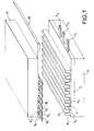
- the plasma display represented on figures 1, 2 and 3 comprises a back glass substrate 10 covered by a dielectric layer 12 in which are embedded row electrodes 14 1 , 14 2 , 14 3 , etc. These electrodes 14 i are parallel to each other and the distance between two neighboring electrodes is constant.
- the inner surface of the back substrate 10 presents ribs 16 1 , 16 2 , 16 3 ... forming partition walls which, in the example, are represented attached to the substrate 10. These ribs may be formed in one piece with the back substrate 10 or with the front substrate.
- ribs 16 1 , 16 2 , 16 3 are perpendicular to electrodes 14 i .
- the distance between two neighboring ribs is constant.
- the interval 24 between two ribs 16 1 and 16 2 forms a groove at the bottom of which is the dielectric layer 12 covered by a phosphor 17. In the direction of the groove there is a succession of red, green and blue phosphors.
- the sidewalls 20, 22 of each groove 24 may be also covered with phosphors (figure 3).
- the panel comprises also a front substrate 26 which is transparent.
- this substrate 26 is made of glass.
- the inner face of this glass substrate 26 is covered with a transparent dielectric layer 28 (figures 1 and 3).
- Column electrodes 30 1 , 30 2 , 30 3 , etc. are embedded in the dielectric layer 28.
- these column electrodes 30 i cover the inner surface 26 1 of the glass substrate 26 and are covered by the transparent layer 28.
- Each column electrode 30 i faces the front edge 32 i of a corresponding partition, or rib, 16 i (figure 3).
- the column electrodes 30 i are facing the partition walls and not the grooves 24, they do not limit the efficiency of the display because they are not situated in front of the phosphors 17 but in the interval between phosphors wherein no light is generated.
- Electrodes 14 could be designated as column electrodes and the electrodes 30 could be designated as row electrodes.
- each column electrode 30 i is parallel to the axis of the corresponding partition wall 16 i but it is shifted towards one of the grooves 24, i.e. away from the other groove 25 (figure 3) on the other side of the partition 16 i .
- the electric field produced by the voltage between a row electrode 14 i and a column electrode 30 i will be higher in the groove 24 than in the groove 25. Therefore, it is possible to generate a discharge in groove 24 without producing a discharge in the neighboring groove 25.
- each column electrode 30 i are attached protrusions or tongues 36 i / 1, 36 i / 2, etc. extending above the cell to be excited.
- the protrusion 36 1 / 1 is above a groove 24. It is made of a transparent material such as ITO (Indium Tin Oxide).
- the length of the tongue 36 1 / 1 is about half the width of the groove between partitions 16 1 and 16 2 .
- each tongues 36 i / j are parallel and above the corresponding pair row electrodes 14 j . In this way, the distance between the tongues 36 and the electrodes 14 is minimized in order to maximize the electric field produced between the column electrodes and the row electrodes.
- column electrodes 30 are not transparent; they can be realized in a metal which has a low resistively and a significant cross section in order to minimize the resistance and, therefore, minimize losses and deformations of the pulses applied to these electrodes.
- the transparent tongues 36 have a higher resistance. However, these tongues do not increase significantly the resistance of the bus or column electrodes.
- the plasma display panel operates as follows:
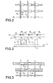
- each cell 40 ij corresponds one row electrode 14j, and one column electrode 30 i (figure 2).
- a high voltage pulse is applied between the electrode 30 i and the electrode 14j, the gas in the cell 40 ij is excited and produces a discharge generating ultraviolet (UV) light.
- UV light excites the phosphors 17.
- the discharge and the UV light is maintained after the disappearance of the pulse by applying a lower AC voltage between the row electrode 14 j and the column electrode 30 i and this UV light disappears when the AC voltage is no more applied between said electrodes.
- This kind of display where the maintenance voltage is produced between row electrodes and column electrodes, is called, as mentioned above, a "matrix type" plasma display panel.
- the plasma display represented on figures 4-7 is of the coplanar type.
- It comprises a back glass substrate 10 covered by a dielectric layer 12 in which are embedded row sustain electrodes 14 11 , 14 12 , 14 21 , 14 23 , etc. These electrodes 14 j1 , 14 j2 , are parallel to each other and form pairs. The distance d (Fig 5) between two electrodes of the same pair is smaller than the distance D between two pairs.
- the inner surface of the back substrate 10 presents ribs 16 1 , 16 2 , 16 3 ... forming partition walls which, in the example, are represented attached to the substrate 10. These ribs may be formed in one piece with the back substrate 10 or with the front substrate.
- ribs 16 1 , 16 2 , 16 3 are perpendicular to electrodes 14 j1 , 14 j2 .
- the distance between two neighboring ribs is constant.
- the interval 24 between two ribs 16 1 and 162 forms a groove at the top of which is a dielectric layer covered by a phosphor 17. In the direction of the groove, there is a succession of red, green and blue phosphors.
- the sidewalls 20, 22 of each groove 24 may be also covered with phosphors.
- the panel comprises also a front substrate 26 which is transparent.
- this substrate 26 is made of glass.
- the inner face of this glass substrate 26 is covered with a transparent dielectric layer 28 which receives the phosphor 17.
- the column electrodes 30 1 , 30 2 , 30 3 , etc. are embedded in the dielectric layer 28.
- these column electrodes 30 i cover the inner surface 26 1 of the glass substrate 26 and are covered by the transparent layer 28.
- Each column electrode 30 i faces the front edge 32 i of a corresponding partition, or rib, 16 i .
- each column electrode 30 i is parallel to the axis of the corresponding partition wall 16 i but it is shifted towards one of the grooves 24, i.e. away from the other groove 25 on the other side of the partition 16 i .
- each tongue 36 i / j is parallel and above the corresponding pair of row electrodes 14 j1 and 14 j2 . In this way, the distance between the tongues 36 and the electrodes 14 is minimized in order to maximize the electric field produced between the column electrodes and the row electrodes.
- the tongue 36 has a width slightly greater than the width d separating the electrodes 14 j1 and 14 j2 but inferior to the width d' separating the two external edges of the electrodes 14 j1 and 14 j2 .
- the electrodes 30 have an axis which is in the medium plane of the partition wall 16. In that case, the correct cell is excited because of the presence of the tongue 36.
- Column electrodes 30 are not transparent; they can be realized in a metal which has a low resistivity and a significant cross section in order to minimize the resistance and, therefore, minimize losses and deformations of the pulses applied to these electrodes.
- the transparent tongues 36 have a higher resistance. However, these tongues do not increase significantly the resistance of the bus or column electrodes.
- the plasma display panel operates as follows:
- each cell 40 ij corresponds two row electrodes 14 j1 and 14 j2 , and one column electrode 30 i .
- a high voltage pulse is applied between the electrode 30 i and the electrode 14 j2 , electric charges are produced on the walls of the cell. These charges constitute seeds for a discharge of the gas (Xe and Ne) inside the cell.
- the gas in the cell 40 ij is excited and produces a discharge generating ultraviolet (UV) light. This UV light excites the phosphors 17. This UV light disappears when the AC voltage is no more applied between said electrodes.
- UV ultraviolet
- the plasma display according to the invention is efficient, i.e. there is no loss of light, because no electrode (or electrodes of minimum area) hides each cell. Moreover, the resistance of the electrodes can be minimized; therefore, there is no degradation of the pulses applied to the electrodes.
Landscapes
- Engineering & Computer Science (AREA)
- Physics & Mathematics (AREA)
- Plasma & Fusion (AREA)
- Chemical & Material Sciences (AREA)
- Materials Engineering (AREA)
- Gas-Filled Discharge Tubes (AREA)
Priority Applications (1)
| Application Number | Priority Date | Filing Date | Title |
|---|---|---|---|
| EP19990400253 EP0945890B1 (fr) | 1998-03-23 | 1999-02-04 | Panneau d'affichage à plasma en courant alternatif |
Applications Claiming Priority (3)
| Application Number | Priority Date | Filing Date | Title |
|---|---|---|---|
| EP98400676 | 1998-03-23 | ||
| EP98400676A EP0945889A1 (fr) | 1998-03-23 | 1998-03-23 | Panneaux d'affichage à plasma |
| EP19990400253 EP0945890B1 (fr) | 1998-03-23 | 1999-02-04 | Panneau d'affichage à plasma en courant alternatif |
Publications (2)
| Publication Number | Publication Date |
|---|---|
| EP0945890A1 true EP0945890A1 (fr) | 1999-09-29 |
| EP0945890B1 EP0945890B1 (fr) | 2003-09-10 |
Family
ID=26151595
Family Applications (1)
| Application Number | Title | Priority Date | Filing Date |
|---|---|---|---|
| EP19990400253 Expired - Lifetime EP0945890B1 (fr) | 1998-03-23 | 1999-02-04 | Panneau d'affichage à plasma en courant alternatif |
Country Status (1)
| Country | Link |
|---|---|
| EP (1) | EP0945890B1 (fr) |
Cited By (2)
| Publication number | Priority date | Publication date | Assignee | Title |
|---|---|---|---|---|
| WO2001075927A1 (fr) * | 2000-04-05 | 2001-10-11 | Thomson Plasma | Panneau a plasma alternatif de type matriciel |
| WO2002058095A1 (fr) * | 2001-01-17 | 2002-07-25 | Matsushita Electric Industrial Co., Ltd. | Ecran d'affichage a plasma et son procede de fabrication |
Citations (3)
| Publication number | Priority date | Publication date | Assignee | Title |
|---|---|---|---|---|
| JPH02168534A (ja) * | 1988-12-20 | 1990-06-28 | Dainippon Printing Co Ltd | プラズマディスプレイパネル |
| US5182489A (en) * | 1989-12-18 | 1993-01-26 | Nec Corporation | Plasma display having increased brightness |
| EP0742571A2 (fr) * | 1995-05-12 | 1996-11-13 | Sony Corporation | Panneau à décharge |
-
1999
- 1999-02-04 EP EP19990400253 patent/EP0945890B1/fr not_active Expired - Lifetime
Patent Citations (3)
| Publication number | Priority date | Publication date | Assignee | Title |
|---|---|---|---|---|
| JPH02168534A (ja) * | 1988-12-20 | 1990-06-28 | Dainippon Printing Co Ltd | プラズマディスプレイパネル |
| US5182489A (en) * | 1989-12-18 | 1993-01-26 | Nec Corporation | Plasma display having increased brightness |
| EP0742571A2 (fr) * | 1995-05-12 | 1996-11-13 | Sony Corporation | Panneau à décharge |
Non-Patent Citations (1)
| Title |
|---|
| PATENT ABSTRACTS OF JAPAN vol. 014, no. 433 (E - 0979) 17 September 1990 (1990-09-17) * |
Cited By (5)
| Publication number | Priority date | Publication date | Assignee | Title |
|---|---|---|---|---|
| WO2001075927A1 (fr) * | 2000-04-05 | 2001-10-11 | Thomson Plasma | Panneau a plasma alternatif de type matriciel |
| FR2807566A1 (fr) * | 2000-04-05 | 2001-10-12 | Thomson Plasma | Perfectionnement au panneau a plasma alternatif de type matriciel |
| WO2002058095A1 (fr) * | 2001-01-17 | 2002-07-25 | Matsushita Electric Industrial Co., Ltd. | Ecran d'affichage a plasma et son procede de fabrication |
| US7329991B2 (en) | 2001-01-17 | 2008-02-12 | Matsushita Electric Industrial Co., Ltd. | Plasma display panel provided with thinned crystal phosphor material and its corresponding method of manufacturing |
| CN100372042C (zh) * | 2001-01-17 | 2008-02-27 | 松下电器产业株式会社 | 等离子体显示屏及其制造方法 |
Also Published As
| Publication number | Publication date |
|---|---|
| EP0945890B1 (fr) | 2003-09-10 |
Similar Documents
| Publication | Publication Date | Title |
|---|---|---|
| US6380678B1 (en) | Plasma display panel | |
| US6806645B2 (en) | Plasma display panel | |
| US6445120B1 (en) | Plasma display panel with improved structure of discharge electrode and dielectric layer | |
| US6515419B1 (en) | Plasma display panel with barriers and electrodes having different widths depending on the discharge cell | |
| US6400082B1 (en) | AC plasma display panel having electrode sets including transparent protrusions | |
| US7750568B2 (en) | Plasma display panel (PDP) having a reflection preventive layer | |
| EP0945890B1 (fr) | Panneau d'affichage à plasma en courant alternatif | |
| KR100323978B1 (ko) | 플라즈마표시장치 | |
| US6380677B1 (en) | Plasma display panel electrode | |
| US6541914B1 (en) | Plasma display panel including grooves in phosphor | |
| US20050264195A1 (en) | Plasma display panel | |
| KR100347226B1 (ko) | 플라즈마 디스플레이 패널 | |
| US6335592B1 (en) | Plasma display panel with specific electrode structures | |
| KR20000009188A (ko) | 플라즈마 디스플레이 패널 | |
| US7375468B2 (en) | Plasma display panel having scan electrode closer to address electrode | |
| KR20040070563A (ko) | 플라즈마 디스플레이 패널 | |
| KR20050088535A (ko) | 플라즈마 디스플레이 패널 | |
| JP2001006564A (ja) | プラズマディスプレイパネル | |
| US20050264233A1 (en) | Plasma display panel (PDP) | |
| KR100686836B1 (ko) | 플라즈마 디스플레이 패널 | |
| US20060076889A1 (en) | Plasma display panel (PDP) | |
| US7525250B2 (en) | Plasma display panel | |
| KR100402745B1 (ko) | 플라즈마 표시장치 | |
| KR100297689B1 (ko) | 플라즈마디스플레이패널 | |
| US20050258754A1 (en) | Plasma display panel |
Legal Events
| Date | Code | Title | Description |
|---|---|---|---|
| PUAI | Public reference made under article 153(3) epc to a published international application that has entered the european phase |
Free format text: ORIGINAL CODE: 0009012 |
|
| AK | Designated contracting states |
Kind code of ref document: A1 Designated state(s): DE FR GB |
|
| AX | Request for extension of the european patent |
Free format text: AL;LT;LV;MK;RO;SI |
|
| 17P | Request for examination filed |
Effective date: 20000316 |
|
| AKX | Designation fees paid |
Free format text: DE FR GB |
|
| 17Q | First examination report despatched |
Effective date: 20021007 |
|
| GRAH | Despatch of communication of intention to grant a patent |
Free format text: ORIGINAL CODE: EPIDOS IGRA |
|
| GRAS | Grant fee paid |
Free format text: ORIGINAL CODE: EPIDOSNIGR3 |
|
| GRAA | (expected) grant |
Free format text: ORIGINAL CODE: 0009210 |
|
| AK | Designated contracting states |
Kind code of ref document: B1 Designated state(s): DE FR GB |
|
| REG | Reference to a national code |
Ref country code: GB Ref legal event code: FG4D |
|
| REF | Corresponds to: |
Ref document number: 69911093 Country of ref document: DE Date of ref document: 20031016 Kind code of ref document: P |
|
| ET | Fr: translation filed | ||
| PLBE | No opposition filed within time limit |
Free format text: ORIGINAL CODE: 0009261 |
|
| STAA | Information on the status of an ep patent application or granted ep patent |
Free format text: STATUS: NO OPPOSITION FILED WITHIN TIME LIMIT |
|
| 26N | No opposition filed |
Effective date: 20040614 |
|
| PGFP | Annual fee paid to national office [announced via postgrant information from national office to epo] |
Ref country code: GB Payment date: 20050111 Year of fee payment: 7 |
|
| PGFP | Annual fee paid to national office [announced via postgrant information from national office to epo] |
Ref country code: DE Payment date: 20050218 Year of fee payment: 7 |
|
| PGFP | Annual fee paid to national office [announced via postgrant information from national office to epo] |
Ref country code: FR Payment date: 20050222 Year of fee payment: 7 |
|
| PG25 | Lapsed in a contracting state [announced via postgrant information from national office to epo] |
Ref country code: GB Free format text: LAPSE BECAUSE OF NON-PAYMENT OF DUE FEES Effective date: 20060204 |
|
| PG25 | Lapsed in a contracting state [announced via postgrant information from national office to epo] |
Ref country code: DE Free format text: LAPSE BECAUSE OF NON-PAYMENT OF DUE FEES Effective date: 20060901 |
|
| GBPC | Gb: european patent ceased through non-payment of renewal fee |
Effective date: 20060204 |
|
| REG | Reference to a national code |
Ref country code: FR Ref legal event code: ST Effective date: 20061031 |
|
| PG25 | Lapsed in a contracting state [announced via postgrant information from national office to epo] |
Ref country code: FR Free format text: LAPSE BECAUSE OF NON-PAYMENT OF DUE FEES Effective date: 20060228 |