EP0945905A3 - FET-Kanalstruktur - Google Patents
FET-Kanalstruktur Download PDFInfo
- Publication number
- EP0945905A3 EP0945905A3 EP99105957A EP99105957A EP0945905A3 EP 0945905 A3 EP0945905 A3 EP 0945905A3 EP 99105957 A EP99105957 A EP 99105957A EP 99105957 A EP99105957 A EP 99105957A EP 0945905 A3 EP0945905 A3 EP 0945905A3
- Authority
- EP
- European Patent Office
- Prior art keywords
- doping
- region
- channel structure
- channel region
- fet channel
- Prior art date
- Legal status (The legal status is an assumption and is not a legal conclusion. Google has not performed a legal analysis and makes no representation as to the accuracy of the status listed.)
- Withdrawn
Links
- 239000002019 doping agent Substances 0.000 abstract 2
- 239000004065 semiconductor Substances 0.000 abstract 2
Classifications
-
- H—ELECTRICITY
- H10—SEMICONDUCTOR DEVICES; ELECTRIC SOLID-STATE DEVICES NOT OTHERWISE PROVIDED FOR
- H10D—INORGANIC ELECTRIC SEMICONDUCTOR DEVICES
- H10D30/00—Field-effect transistors [FET]
- H10D30/01—Manufacture or treatment
- H10D30/021—Manufacture or treatment of FETs having insulated gates [IGFET]
- H10D30/0221—Manufacture or treatment of FETs having insulated gates [IGFET] having asymmetry in the channel direction, e.g. lateral high-voltage MISFETs having drain offset region or extended-drain MOSFETs [EDMOS]
-
- H—ELECTRICITY
- H10—SEMICONDUCTOR DEVICES; ELECTRIC SOLID-STATE DEVICES NOT OTHERWISE PROVIDED FOR
- H10D—INORGANIC ELECTRIC SEMICONDUCTOR DEVICES
- H10D30/00—Field-effect transistors [FET]
- H10D30/60—Insulated-gate field-effect transistors [IGFET]
- H10D30/63—Vertical IGFETs
-
- H—ELECTRICITY
- H10—SEMICONDUCTOR DEVICES; ELECTRIC SOLID-STATE DEVICES NOT OTHERWISE PROVIDED FOR
- H10D—INORGANIC ELECTRIC SEMICONDUCTOR DEVICES
- H10D62/00—Semiconductor bodies, or regions thereof, of devices having potential barriers
- H10D62/10—Shapes, relative sizes or dispositions of the regions of the semiconductor bodies; Shapes of the semiconductor bodies
- H10D62/17—Semiconductor regions connected to electrodes not carrying current to be rectified, amplified or switched, e.g. channel regions
- H10D62/213—Channel regions of field-effect devices
- H10D62/221—Channel regions of field-effect devices of FETs
- H10D62/235—Channel regions of field-effect devices of FETs of IGFETs
- H10D62/292—Non-planar channels of IGFETs
-
- H—ELECTRICITY
- H10—SEMICONDUCTOR DEVICES; ELECTRIC SOLID-STATE DEVICES NOT OTHERWISE PROVIDED FOR
- H10D—INORGANIC ELECTRIC SEMICONDUCTOR DEVICES
- H10D62/00—Semiconductor bodies, or regions thereof, of devices having potential barriers
- H10D62/10—Shapes, relative sizes or dispositions of the regions of the semiconductor bodies; Shapes of the semiconductor bodies
- H10D62/17—Semiconductor regions connected to electrodes not carrying current to be rectified, amplified or switched, e.g. channel regions
- H10D62/213—Channel regions of field-effect devices
- H10D62/221—Channel regions of field-effect devices of FETs
- H10D62/235—Channel regions of field-effect devices of FETs of IGFETs
- H10D62/299—Channel regions of field-effect devices of FETs of IGFETs having lateral doping variations
- H10D62/307—Channel regions of field-effect devices of FETs of IGFETs having lateral doping variations the doping variations being parallel to the channel lengths
Landscapes
- Insulated Gate Type Field-Effect Transistor (AREA)
- Thin Film Transistor (AREA)
Abstract
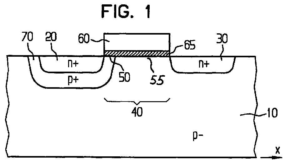
Applications Claiming Priority (2)
| Application Number | Priority Date | Filing Date | Title |
|---|---|---|---|
| DE19812945A DE19812945A1 (de) | 1998-03-24 | 1998-03-24 | Halbleiterbauelement und Verfahren zu dessen Herstellung |
| DE19812945 | 1998-03-24 |
Publications (2)
| Publication Number | Publication Date |
|---|---|
| EP0945905A2 EP0945905A2 (de) | 1999-09-29 |
| EP0945905A3 true EP0945905A3 (de) | 2000-01-12 |
Family
ID=7862150
Family Applications (1)
| Application Number | Title | Priority Date | Filing Date |
|---|---|---|---|
| EP99105957A Withdrawn EP0945905A3 (de) | 1998-03-24 | 1999-03-24 | FET-Kanalstruktur |
Country Status (2)
| Country | Link |
|---|---|
| EP (1) | EP0945905A3 (de) |
| DE (1) | DE19812945A1 (de) |
Citations (5)
| Publication number | Priority date | Publication date | Assignee | Title |
|---|---|---|---|---|
| JPH0260131A (ja) * | 1988-08-26 | 1990-02-28 | Matsushita Electric Works Ltd | 電界効果半導体装置の製造方法 |
| EP0402296A1 (de) * | 1989-06-09 | 1990-12-12 | International Business Machines Corporation | Feldeffekttransistor mit asymmetrischer Struktur |
| US5021845A (en) * | 1985-08-30 | 1991-06-04 | Texas Instruments Incorporated | Semiconductor device and process fabrication thereof |
| US5233215A (en) * | 1992-06-08 | 1993-08-03 | North Carolina State University At Raleigh | Silicon carbide power MOSFET with floating field ring and floating field plate |
| EP0752722A2 (de) * | 1995-07-07 | 1997-01-08 | Motorola, Inc. | FET mit stabiler Schwellwertspannung und dessen Herstellungsverfahren |
-
1998
- 1998-03-24 DE DE19812945A patent/DE19812945A1/de not_active Withdrawn
-
1999
- 1999-03-24 EP EP99105957A patent/EP0945905A3/de not_active Withdrawn
Patent Citations (5)
| Publication number | Priority date | Publication date | Assignee | Title |
|---|---|---|---|---|
| US5021845A (en) * | 1985-08-30 | 1991-06-04 | Texas Instruments Incorporated | Semiconductor device and process fabrication thereof |
| JPH0260131A (ja) * | 1988-08-26 | 1990-02-28 | Matsushita Electric Works Ltd | 電界効果半導体装置の製造方法 |
| EP0402296A1 (de) * | 1989-06-09 | 1990-12-12 | International Business Machines Corporation | Feldeffekttransistor mit asymmetrischer Struktur |
| US5233215A (en) * | 1992-06-08 | 1993-08-03 | North Carolina State University At Raleigh | Silicon carbide power MOSFET with floating field ring and floating field plate |
| EP0752722A2 (de) * | 1995-07-07 | 1997-01-08 | Motorola, Inc. | FET mit stabiler Schwellwertspannung und dessen Herstellungsverfahren |
Non-Patent Citations (6)
| Title |
|---|
| BUTI T N ET AL: "A NEW ASYMMETRICAL HALO SOURCE GOLD DRAIN (HS-GOLD) DEEP SUB-HALF -MICROMETER N-MOSFET DESIGN FOR RELIABILITY AND PERFORMANCE", IEEE TRANSACTIONS ON ELECTRON DEVICES, vol. 38, no. 8, 1 August 1991 (1991-08-01), pages 1757 - 1764, XP000217059, ISSN: 0018-9383 * |
| DECELERCQ M J ET AL: "A theoretical and experimental study of DMOS enhancement/depletion logic", IEEE JOURNAL OF SOLID-STATE CIRCUITS, JUNE 1977, USA, vol. SC-12, no. 3, pages 264 - 270, XP002121754, ISSN: 0018-9200 * |
| PATENT ABSTRACTS OF JAPAN vol. 014, no. 229 (E - 0928) 15 May 1990 (1990-05-15) * |
| RODGERS T J ET AL: "An experimental and theoretical analysis of double-diffused MOS transistors", IEEE JOURNAL OF SOLID-STATE CIRCUITS, OCT. 1975, USA, vol. SC-10, no. 5, pages 322 - 331, XP002121753, ISSN: 0018-9200 * |
| SHEN C -C ET AL: "USE OF FOCUSED-ION-BEAM AND MODELING TO OPTIMIZE SUBMICRON MOSFET CHARACTERISTICS", IEEE TRANSACTIONS ON ELECTRON DEVICES, vol. 45, no. 2, 1 February 1998 (1998-02-01), pages 453 - 459, XP000734684, ISSN: 0018-9383 * |
| YOSHINORI OKUMURA ET AL: "SOURCE-TO-DRAIN NONUNIFORMLY DOPED CHANNEL (NUDC) MOSFET STRUCTURES FOR HIGH CURRENT DRIVABILITY AND THRESHOLD VOLTAGE CONTROLLABILITY", IEEE TRANSACTIONS ON ELECTRON DEVICES, vol. 39, no. 11, 1 November 1992 (1992-11-01), pages 2541 - 2552, XP000321695, ISSN: 0018-9383 * |
Also Published As
| Publication number | Publication date |
|---|---|
| EP0945905A2 (de) | 1999-09-29 |
| DE19812945A1 (de) | 1999-09-30 |
Similar Documents
| Publication | Publication Date | Title |
|---|---|---|
| DE60033271T2 (de) | Laterales dünnfilm-silizium-auf-isolator-(soi)-pmos-bauelement mit drain-ausdehnungszone | |
| DE69224709T2 (de) | Halbleiteranordnung mit verbesserter Durchbruchspannungs-Charakteristik | |
| DE69520782T2 (de) | Randabschlussmethode und Struktur für Leistungs-MOSFET | |
| DE60222751T2 (de) | Feldeffekttransistorstruktur und herstellungsverfahren | |
| DE2611338C3 (de) | Feldeffekttransistor mit sehr kurzer Kanallange | |
| DE69937101T2 (de) | Laterale-dünnfilm-silizium-auf-isolator (soi) anordnung mit mehreren gebieten im drift-gebiet | |
| WO2004040656A1 (de) | Mos-transistor auf soi-substrat mit source-durchkontaktierung | |
| DE69533134T2 (de) | Leistungsbauteil hoher Dichte in MOS-Technologie | |
| EP1181712B1 (de) | Niederohmiges vdmos-halbleiterbauelement | |
| EP2503612A2 (de) | Vertikaler Hallsensor und Verfahren zur Herstellung eines vertikalen Hallsensors | |
| AT505176A2 (de) | Grabenfeldplattenabschluss für leistungsvorrichtungen | |
| DE19733974C2 (de) | MOSFET-Einrichtung und Verfahren zur Herstellung | |
| DE10229146A1 (de) | Laterales Superjunction-Halbleiterbauteil | |
| DE10224003B4 (de) | Halbleitervorrichtung und Verfahren für ihre Herstellung | |
| DE10127950B4 (de) | Verfahren zur Herstellung eines Halbleiterbauelements und Halbleiterbauelement | |
| DE69014454T2 (de) | Hochspannungs-Halbleiteranordnung und Verfahren zur Herstellung. | |
| EP1336989B1 (de) | Transistorbauelement | |
| DE19604044C2 (de) | Durch Feldeffekt steuerbares Halbleiterbauelement | |
| EP1584904B1 (de) | Photomischdetektor | |
| DE10112783B4 (de) | Halbleiteranordnung mit einem Leistungs-MOSFET und einem Widerstandselement | |
| DE69033647T2 (de) | Methode zur Herstellung einer Halbleiterstruktur für integrierte Hochleistungsschaltungen | |
| DE10310552B4 (de) | Feldeffekttransistor und Halbleiterchip mit diesem Feldeffekttransistor | |
| DE4441901C2 (de) | MOSFET auf SOI-Substrat und Verfahren zu dessen Herstellung | |
| EP0973204A3 (de) | MOS-Transistor mit hoher Spannungsfestigkeit und niedrigem Einschaltwiderstand | |
| DE69606932T2 (de) | MOS-Kapazität für Halbleiteranordnung |
Legal Events
| Date | Code | Title | Description |
|---|---|---|---|
| PUAI | Public reference made under article 153(3) epc to a published international application that has entered the european phase |
Free format text: ORIGINAL CODE: 0009012 |
|
| AK | Designated contracting states |
Kind code of ref document: A2 Designated state(s): DE FR GB IE IT |
|
| AX | Request for extension of the european patent |
Free format text: AL;LT;LV;MK;RO;SI |
|
| PUAL | Search report despatched |
Free format text: ORIGINAL CODE: 0009013 |
|
| RIC1 | Information provided on ipc code assigned before grant |
Free format text: 7H 01L 29/78 A, 7H 01L 29/10 B, 7H 01L 21/336 B |
|
| AK | Designated contracting states |
Kind code of ref document: A3 Designated state(s): AT BE CH CY DE DK ES FI FR GB GR IE IT LI LU MC NL PT SE |
|
| AX | Request for extension of the european patent |
Free format text: AL;LT;LV;MK;RO;SI |
|
| 17P | Request for examination filed |
Effective date: 20000711 |
|
| AKX | Designation fees paid |
Free format text: DE FR GB IE IT |
|
| STAA | Information on the status of an ep patent application or granted ep patent |
Free format text: STATUS: THE APPLICATION HAS BEEN WITHDRAWN |
|
| 18W | Application withdrawn |
Withdrawal date: 20000804 |