EP0946792B1 - Procede de fabrication d'un element de construction micromecanique - Google Patents
Procede de fabrication d'un element de construction micromecanique Download PDFInfo
- Publication number
- EP0946792B1 EP0946792B1 EP97912034A EP97912034A EP0946792B1 EP 0946792 B1 EP0946792 B1 EP 0946792B1 EP 97912034 A EP97912034 A EP 97912034A EP 97912034 A EP97912034 A EP 97912034A EP 0946792 B1 EP0946792 B1 EP 0946792B1
- Authority
- EP
- European Patent Office
- Prior art keywords
- layer
- layers
- resist
- regions
- sputtered
- Prior art date
- Legal status (The legal status is an assumption and is not a legal conclusion. Google has not performed a legal analysis and makes no representation as to the accuracy of the status listed.)
- Expired - Lifetime
Links
- 238000004519 manufacturing process Methods 0.000 title claims abstract description 31
- 229910052751 metal Inorganic materials 0.000 claims abstract description 18
- 239000002184 metal Substances 0.000 claims abstract description 18
- 238000001465 metallisation Methods 0.000 claims abstract description 13
- 239000007769 metal material Substances 0.000 claims abstract description 5
- 239000010410 layer Substances 0.000 claims description 153
- 238000000034 method Methods 0.000 claims description 36
- 239000000758 substrate Substances 0.000 claims description 29
- RTAQQCXQSZGOHL-UHFFFAOYSA-N Titanium Chemical compound [Ti] RTAQQCXQSZGOHL-UHFFFAOYSA-N 0.000 claims description 8
- 238000005530 etching Methods 0.000 claims description 7
- 239000010936 titanium Substances 0.000 claims description 7
- 229910052719 titanium Inorganic materials 0.000 claims description 7
- KDLHZDBZIXYQEI-UHFFFAOYSA-N Palladium Chemical compound [Pd] KDLHZDBZIXYQEI-UHFFFAOYSA-N 0.000 claims description 6
- KRHYYFGTRYWZRS-UHFFFAOYSA-N Fluorane Chemical compound F KRHYYFGTRYWZRS-UHFFFAOYSA-N 0.000 claims description 4
- 229920002120 photoresistant polymer Polymers 0.000 claims description 4
- 229910052763 palladium Inorganic materials 0.000 claims description 3
- 239000004033 plastic Substances 0.000 claims description 3
- 238000006479 redox reaction Methods 0.000 claims description 2
- 238000004070 electrodeposition Methods 0.000 claims 8
- 239000011229 interlayer Substances 0.000 claims 8
- 239000002904 solvent Substances 0.000 claims 1
- 238000007730 finishing process Methods 0.000 abstract 1
- 229910052755 nonmetal Inorganic materials 0.000 abstract 1
- 238000009713 electroplating Methods 0.000 description 34
- 238000001459 lithography Methods 0.000 description 7
- 230000004913 activation Effects 0.000 description 5
- 239000000463 material Substances 0.000 description 5
- 238000004544 sputter deposition Methods 0.000 description 5
- PXHVJJICTQNCMI-UHFFFAOYSA-N Nickel Chemical compound [Ni] PXHVJJICTQNCMI-UHFFFAOYSA-N 0.000 description 4
- 239000004922 lacquer Substances 0.000 description 4
- QVGXLLKOCUKJST-UHFFFAOYSA-N atomic oxygen Chemical compound [O] QVGXLLKOCUKJST-UHFFFAOYSA-N 0.000 description 3
- 150000002500 ions Chemical class 0.000 description 3
- 239000001301 oxygen Substances 0.000 description 3
- 229910052760 oxygen Inorganic materials 0.000 description 3
- 238000005240 physical vapour deposition Methods 0.000 description 3
- 238000007789 sealing Methods 0.000 description 3
- 238000007704 wet chemistry method Methods 0.000 description 3
- XKRFYHLGVUSROY-UHFFFAOYSA-N Argon Chemical compound [Ar] XKRFYHLGVUSROY-UHFFFAOYSA-N 0.000 description 2
- 239000004642 Polyimide Substances 0.000 description 2
- XUIMIQQOPSSXEZ-UHFFFAOYSA-N Silicon Chemical compound [Si] XUIMIQQOPSSXEZ-UHFFFAOYSA-N 0.000 description 2
- 239000011248 coating agent Substances 0.000 description 2
- 238000000576 coating method Methods 0.000 description 2
- 238000011161 development Methods 0.000 description 2
- 230000018109 developmental process Effects 0.000 description 2
- 239000003792 electrolyte Substances 0.000 description 2
- 238000005516 engineering process Methods 0.000 description 2
- 230000035784 germination Effects 0.000 description 2
- 239000011521 glass Substances 0.000 description 2
- 229910052759 nickel Inorganic materials 0.000 description 2
- BASFCYQUMIYNBI-UHFFFAOYSA-N platinum Chemical compound [Pt] BASFCYQUMIYNBI-UHFFFAOYSA-N 0.000 description 2
- 229920001721 polyimide Polymers 0.000 description 2
- 229910052710 silicon Inorganic materials 0.000 description 2
- 239000010703 silicon Substances 0.000 description 2
- RYGMFSIKBFXOCR-UHFFFAOYSA-N Copper Chemical compound [Cu] RYGMFSIKBFXOCR-UHFFFAOYSA-N 0.000 description 1
- BQCADISMDOOEFD-UHFFFAOYSA-N Silver Chemical compound [Ag] BQCADISMDOOEFD-UHFFFAOYSA-N 0.000 description 1
- 230000002378 acidificating effect Effects 0.000 description 1
- 230000001464 adherent effect Effects 0.000 description 1
- 229910052786 argon Inorganic materials 0.000 description 1
- 230000015572 biosynthetic process Effects 0.000 description 1
- 239000000919 ceramic Substances 0.000 description 1
- 238000010276 construction Methods 0.000 description 1
- 229910052802 copper Inorganic materials 0.000 description 1
- 239000010949 copper Substances 0.000 description 1
- 238000007598 dipping method Methods 0.000 description 1
- 230000005611 electricity Effects 0.000 description 1
- 229910052731 fluorine Inorganic materials 0.000 description 1
- 239000011737 fluorine Substances 0.000 description 1
- 239000007789 gas Substances 0.000 description 1
- 238000010849 ion bombardment Methods 0.000 description 1
- 238000003754 machining Methods 0.000 description 1
- 230000000873 masking effect Effects 0.000 description 1
- 150000002739 metals Chemical class 0.000 description 1
- 239000000203 mixture Substances 0.000 description 1
- 230000006911 nucleation Effects 0.000 description 1
- 238000010899 nucleation Methods 0.000 description 1
- 238000010422 painting Methods 0.000 description 1
- 229910052697 platinum Inorganic materials 0.000 description 1
- 238000002360 preparation method Methods 0.000 description 1
- 230000002787 reinforcement Effects 0.000 description 1
- 239000004065 semiconductor Substances 0.000 description 1
- 229910052709 silver Inorganic materials 0.000 description 1
- 239000004332 silver Substances 0.000 description 1
- 229910000033 sodium borohydride Inorganic materials 0.000 description 1
- 239000012279 sodium borohydride Substances 0.000 description 1
- 239000007787 solid Substances 0.000 description 1
- 238000009987 spinning Methods 0.000 description 1
- 239000007921 spray Substances 0.000 description 1
- 238000005507 spraying Methods 0.000 description 1
- 239000000126 substance Substances 0.000 description 1
- 239000002344 surface layer Substances 0.000 description 1
- 238000007740 vapor deposition Methods 0.000 description 1
- 235000012431 wafers Nutrition 0.000 description 1
Images


Classifications
-
- C—CHEMISTRY; METALLURGY
- C25—ELECTROLYTIC OR ELECTROPHORETIC PROCESSES; APPARATUS THEREFOR
- C25D—PROCESSES FOR THE ELECTROLYTIC OR ELECTROPHORETIC PRODUCTION OF COATINGS; ELECTROFORMING; APPARATUS THEREFOR
- C25D1/00—Electroforming
- C25D1/003—3D structures, e.g. superposed patterned layers
-
- H—ELECTRICITY
- H10—SEMICONDUCTOR DEVICES; ELECTRIC SOLID-STATE DEVICES NOT OTHERWISE PROVIDED FOR
- H10D—INORGANIC ELECTRIC SEMICONDUCTOR DEVICES
- H10D48/00—Individual devices not covered by groups H10D1/00 - H10D44/00
- H10D48/50—Devices controlled by mechanical forces, e.g. pressure
-
- C—CHEMISTRY; METALLURGY
- C25—ELECTROLYTIC OR ELECTROPHORETIC PROCESSES; APPARATUS THEREFOR
- C25D—PROCESSES FOR THE ELECTROLYTIC OR ELECTROPHORETIC PRODUCTION OF COATINGS; ELECTROFORMING; APPARATUS THEREFOR
- C25D5/00—Electroplating characterised by the process; Pretreatment or after-treatment of workpieces
- C25D5/02—Electroplating of selected surface areas
- C25D5/022—Electroplating of selected surface areas using masking means
-
- H—ELECTRICITY
- H01—ELECTRIC ELEMENTS
- H01H—ELECTRIC SWITCHES; RELAYS; SELECTORS; EMERGENCY PROTECTIVE DEVICES
- H01H1/00—Contacts
- H01H1/0036—Switches making use of microelectromechanical systems [MEMS]
Definitions
- the invention relates to a method for producing a micromechanical component consisting of several layers, for example from electrically conductive and non-conductive Layers or areas or from layers or areas metallic and non-metallic materials, according to the preamble of the main claim.
- microsensor as a micromechanical Component known in which component structures layers arranged one above the other have been obtained.
- a copper layer was used as Sputter layer for a start metallization for one above to be arranged electroplating layer used.
- micro valve As a micro valve
- the component used are individual layers in the structure of the Micro valve with micromechanical manufacturing methods processed.
- the surface of a Silicon wafers structured and photolithographically through Subsequent etching predefined areas become partial removed so that the desired mechanical elements through a structured three-dimensional processing of these layers be formed.
- UV deep lithography is one of the manufacturing processes for structuring the non-conducting areas and multi-layer electroplating for the production of metallic, managerial areas known for themselves.
- a conductive starting layer on non-conductive carrier layers for the later external galvanic Metal deposition required in the respective areas is also a conductive starting layer on non-conductive carrier layers for the later external galvanic Metal deposition required in the respective areas.
- the manufacturing method for a Micromechanical component of the type mentioned is in the training with the features of the main claim thereby advantageous that for multi-layer electroplating Start metallizations are applied to the rest Processes and materials of UV depth lithography and
- Multi-layer electroplating are compatible.
- the invention Start metallization enables the new electroplating to adhere firmly to the bottom and thus three-dimensionally structured components in layered construction enable.
- the Start metallization designed such that in certain Areas of the substrate as a starting layer with a layer low liability is present. Then in these areas the top electroplating layer can be lifted off the bottom and it can move components with an arbitrarily narrow gap be created between their contact surfaces. Examples are sealing elements for fluidic applications or Switching elements that are closed in the non-actuated state are.
- the manufacturing method according to the invention allows in particular a further development of the manufacturing process with UV depth lithography and multilayer electroplating for the production of Components with three-dimensional structures and with Undercuts.
- This is made possible by the electrical conductive intermediate layers that allow metals electrolytic, i.e. external current on surfaces with Structures made of metal and electrically insulating plastic deposit.
- the metallic areas of each The surface of the layers usually consist of a lower one Galvanic layer, the insulating areas from one photostructured resist (e.g. polyimide, AZ lacquer (photoresist) or permanent resists).
- Applications of the component according to the invention are three-dimensional micro components made of metal with Undercuts such as turbulence nozzles for the Mixture preparation in gasoline engines or also microsensors or Components that also have movable structures such as Micro valves, micro relays, micro switches or micro motors.
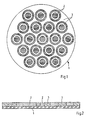
- a Micromechanical component can be seen, namely a substrate 1 as a carrier layer for further layers to be applied.
- the substrate can be metal, silicon, ceramic or glass; at the The embodiment described here is made of glass.
- the Typical thicknesses of this substrate are between 500 ⁇ m and 2 mm and it must, in particular to external currents to enable galvanic processes to adhere well to metallic ones Starting layers can be applied.
- the substrate 1 is connected in a known manner conductive areas 2 and with non-conductive areas 3 Mistake.
- the substrate is coated with a resist (e.g. Polyimide, AZ lacquer or solid resist) coated by Spin on, spray or laminate.
- the resist is with the desired structure exposed and developed.
- the coating (resist) is then galvanized metal deposited.
- the conductive areas 2 of the lower Electroplating layer consist of a metallic material (e.g. Copper or nickel), the non-conductive areas 3 from the Resist. In Figure 2, these areas 2 and 3 are on average detect.
- a first Manufacturing step is the entire surface of the Substrate 1 together with regions 2 and 3 with a layer 4 sputtered from silver, palladium or platinum; with the described This layer of palladium is an exemplary embodiment.
- the process of sputtering is known per se; here is out the so-called target with an ionized gas (e.g. argon) bombarded with high-energy ions.
- the target is replaced by the ion bombardment atoms and / or molecules knocked out and with 1/100 of the kinetic energy of the ions on the substrate 1 accelerated.
- a very thin layer is thus formed on the substrate 1 even new surface layer.
- the thickness of the layer 4 is a few nanometers if this sputter layer 4 as Germination layer for a subsequently external currentless (i.e. metallic starting layer applied by metal deposition) should function, and 5 nm to 100 nm if the sputter layer 4 even as a starting layer for the following external current galvanic processes should serve.
- This Step is advantageous with one in the so-called Multi-layer electroplating for a standard process known per se (electrolytic activation) carried out in which the previously resulting arrangement with a non-passivating Electrolytes (e.g. Ni-Strike bath containing C1 ions) treated , then the conductive areas 2 by a few micrometers can be removed anodically under the sputter layer 4.
- Electrolytes e.g. Ni-Strike bath containing C1 ions
- the sputter layer 4 is not used in this manufacturing step removed, but loses liability to the lower one Metal layer of areas 2 and can in a rinsing step this metal layer can be removed and removed.
- the non-conductive areas 3 are thus coated to fit without that one with new lateral tolerances photolithographic structuring would have been necessary (View c) of Figure 3).
- the next one, also from view d) of FIG. 3 visible manufacturing step are the exposed Areas of the sputter layer 4 and the exposed areas the lower electroplating layer 2 chemically, i.e. in a Redox reaction without external current with a metal (e.g. nickel) reinforced or coated (visible only in the left part of the View d)).
- a metal e.g. nickel
- the bottom electroplating layer (Areas 2) activated again by anodic removal and the sputter layer 4 in a reducing bath (e.g. with Sodium borohydride) also activated.
- a reducing bath e.g. with Sodium borohydride
- the metallic galvanic layers 2 and 7 thus adhere to the chemically deposited layer 6 to each other and can a detachment from the substrate 1 and the removal of the Resist layers 3 and 5, according to view f) of FIG. 3 micromechanical component with complex structures including forming undercuts.
- Electroplating layer 7 are deposited (right side of Fig. 3d) and 3e)).
- the material of the metal layer 6 deposited without external current should because of the desired chemical homogeneity and a better adhesion of layers 2, 6 and 7 to each other electrodeposited metal of layers 2 and 7 be as similar as possible chemically. With a thicker one Sputter layer 4 can be applied to the external currentless metallic reinforcement can be dispensed with (as above ) Described.
- the photoresist of the areas 5 for structuring the top Electroplating layer 7 is preferably used before activation of the lower metal layer in areas 2 and the sputter layer 4 can be applied.
- the advantage is that the Activation step only needs to be carried out once.
- the disadvantage is that the lacquer structures of the photoresist in the Areas 5 may be underestimated.
- the substrate 1 has View a) again metallic, electrically conductive areas 2 in addition to electrically non-conductive areas 3.
- the Metallic areas 2 can, for example, from the lower Electroplating and the non-conductive areas from one through the known resist structured with UV depth lithography be formed.
- the substrate 1 In a first production step, the substrate 1 all over, as described above, but in this case with Titan sputtered.
- the thickness of this sputter layer 10 is 200 nm to 400 nm.
- the manufacturing step is to be carried out that the titanium sputter layer 10 has as little oxygen as possible contains and thus also forms as little stable oxide as possible, because only in this way can it be etched in the next process step be structured (view b)). It is therefore necessary a good vacuum around the substrate 1 before sputtering to manufacture and the substrate 1 first by an etching process (also using sputter technology).
- the lower one Electroplating layer 2 is said to have a smooth surface have low oxygen surface coverage.
- the sputtered titanium layer 10 is in accordance with view b) masked in a photostructurable lacquer and in one Hydrogen-fluorine-containing solution (hydrofluoric acid) etched.
- a resist 11 in media can be processed on the plastic or resist 3 do not attack the substrate 1.
- an arrangement is created according to view c) 3 and the further process steps of Multi-layer electroplating can be carried out.
- galvanic layers can be used are formed between structured resist regions 11a. At the At the end of the process chain, the resist 11a is removed. All over where two metallic galvanic layers 2, 12 by one Titanium sputter layer 10 are separated, the two Layers 2 and 12 by applying a mechanical force or a differential pressure can be separated.
- Electroplating layers 2 and 12 can be removed. Neither arises Gap between the two mechanically separated Galvanolayers 2 and 12.
- the surface morphology of the lower electroplating layer 2 is applied to the upper electroplating layer 12 mapped so that micromechanical components with moving Parts (view e)) can be manufactured, the sealing can lie together.
Landscapes
- Chemical & Material Sciences (AREA)
- Engineering & Computer Science (AREA)
- Chemical Kinetics & Catalysis (AREA)
- Electrochemistry (AREA)
- Materials Engineering (AREA)
- Metallurgy (AREA)
- Organic Chemistry (AREA)
- Crystallography & Structural Chemistry (AREA)
- Micromachines (AREA)
- Electroplating Methods And Accessories (AREA)
- Physical Vapour Deposition (AREA)
Abstract
Claims (6)
- Procédé de fabrication d'un composant micromécanique ayant les caractéristiques suivantes :le composant micromécanique comporte des couches superposées de matières métalliques, les couches étant accrochées solidairement au moins en partie et reliées l'une à l'autre par des couches intermédiaires (4, 6) au moins pendant le procédé de fabrication,
les couches intermédiaires étant au moins constituées par une couche pulvérisée (4) appliquée comme métallisation de départ sur chaque couche métallique intérieure (2) et sur laquelle on peut appliquer une couche galvanique métallique supérieure, ayant les étapes suivantes :sur un substrat (1), on applique comme couche de support une première couche avec des zones conductrices (2) et des zones non-conductrices (3),sur la première couche, on applique une couche de pulvérisation (4) comme couche intermédiaire,la couche de pulvérisation (4) est attaquée par en dessous du fait de sa porosité dans les zones conductrices (2) et ensuite on l'enlève,on applique un résist supérieur (5) sur les zones qui restent de la couche pulvérisée (4) et sur les zones conductrices (2),dans les zones libres, entre le résist (5), on applique par galvanoplastie une couche métallique supérieure (7) etdans une autre étape de fabrication, on enlève le substrat (1), les zones non-conductrices (3) et la couche supérieure de résist (5). - Procédé de fabrication d'un composant de micromécanique selon la revendication 1,
caractérisé en ce que
la couche pulvérisée (4) a une épaisseur de 5 nm jusqu'à 100 nm. - Procédé de fabrication d'un composant de micromécanique selon la revendication 1,
caractérisé en ce quepour réaliser la couche intermédiaire (6), on a une couche pulvérisée (4) ayant une épaisseur de 5 nm jusqu'à 10 nm et on active cette couche chimiquement par une réaction Redox pour qu'elle reçoive du métal, les zones conductrices (2) de la couche galvanique inférieure étant activées chimiquement par enlèvement anodique etensuite, on applique la couche galvanique supérieure (7) sur la couche intermédiaire (6). - Procédé de fabrication d'un composant de micromécanique selon l'une des revendications 1 à 3,
caractérisé en ce que
la couche pulvérisée (4) est du palladium. - Procédé de fabrication d'un composant micromécanique ayant les caractéristiques suivantes :le composant micromécanique comporte des couches superposées formées de matières métalliques, les couches s'accrochant au moins partiellement solidairement les unes aux autres et étant reliées les unes aux autres au moins pendant le procédé de fabrication par des couches intermédiaires (10), les couches intermédiaires étant constituées par au moins une couche pulvérisée (10), appliquée comme métallisation de départ sur la couche métallique (2) respectivement en dessous et sur laquelle on applique une couche galvanique métallique (7), au-dessus, procédé comprenant les étapes suivantes :on applique sur un substrat (1) comme couche de support une première couche avec des zones conductrices (2) et des zones non-conductrices (3),on applique une couche pulvérisée (10) en titane comme couche intermédiaire sur la première couche,on masque la couche pulvérisée (10) avec un résist (11),on enlève par attaque chimique la couche pulvérisée (10) dans les zones non masquées et ensuite on enlève le résist (10),dans des zones prédéterminées, on applique un autre résist (11a) et dans les zones entre l'autre résist (11a) on applique par galvanoplastie une couche galvanique supérieure (12), etdans une étape de fabrication ultérieure, on enlève le substrat (1), les zones non-conductrices (3) et le résist (11a) et on enlève, des zones conductrices (2), la couche galvanique supérieure (12) de la couche pulvérisée (10).
- Procédé de fabrication d'un composant micromécanique selon la revendication 5,
caractérisé en ce que
le résist (11), utilisé comme masque pour la couche pulvérisée (10), est attaqué avec une photolaque (AZ-laque) traité avec des solvants et dans une solution d'acide fluorhydrique, les zones non-conductrices (3) de la couche de support étant en une matière plastique que l'on peut traiter dans un milieu alcalin aqueux.
Applications Claiming Priority (3)
| Application Number | Priority Date | Filing Date | Title |
|---|---|---|---|
| DE19641531A DE19641531A1 (de) | 1996-10-09 | 1996-10-09 | Mikromechanisches Bauelement und ein Verfahren zu dessen Herstellung |
| DE19641531 | 1996-10-09 | ||
| PCT/DE1997/002230 WO1998015676A1 (fr) | 1996-10-09 | 1997-09-29 | Element de construction micromecanique et procede de fabrication |
Publications (2)
| Publication Number | Publication Date |
|---|---|
| EP0946792A1 EP0946792A1 (fr) | 1999-10-06 |
| EP0946792B1 true EP0946792B1 (fr) | 2003-05-02 |
Family
ID=7808218
Family Applications (1)
| Application Number | Title | Priority Date | Filing Date |
|---|---|---|---|
| EP97912034A Expired - Lifetime EP0946792B1 (fr) | 1996-10-09 | 1997-09-29 | Procede de fabrication d'un element de construction micromecanique |
Country Status (7)
| Country | Link |
|---|---|
| US (1) | US6174416B1 (fr) |
| EP (1) | EP0946792B1 (fr) |
| JP (1) | JP4130230B2 (fr) |
| KR (1) | KR100482911B1 (fr) |
| DE (2) | DE19641531A1 (fr) |
| ES (1) | ES2198558T3 (fr) |
| WO (1) | WO1998015676A1 (fr) |
Families Citing this family (8)
| Publication number | Priority date | Publication date | Assignee | Title |
|---|---|---|---|---|
| US6236139B1 (en) * | 1999-02-26 | 2001-05-22 | Jds Uniphase Inc. | Temperature compensated microelectromechanical structures and related methods |
| US6670208B2 (en) * | 2000-06-23 | 2003-12-30 | Nec Corporation | Optical circuit in which fabrication is easy |
| US6829079B2 (en) | 2000-12-22 | 2004-12-07 | Nec Corporation | Optical path control apparatus with mirror section, and manufacturing method for the same |
| US20060073348A1 (en) * | 2004-10-06 | 2006-04-06 | General Electric Company | Electroplated fuel nozzle/swirler wear coat |
| GB2432847A (en) * | 2005-12-02 | 2007-06-06 | Microstencil Ltd | Electroformed component manufacture |
| EP1835050A1 (fr) * | 2006-03-15 | 2007-09-19 | Doniar S.A. | Procédé de fabrication par LIGA-UV d'une structure métallique multicouche à couches adjacentes non entièrement superposées, et structure obtenue |
| EP3231898B1 (fr) * | 2014-12-12 | 2019-10-09 | Citizen Watch Co., Ltd. | Procédé permettant de fabriquer des composants électroformés |
| CN106989499A (zh) * | 2017-02-08 | 2017-07-28 | 福建省锐驰电子科技有限公司 | 一种具有金属质感的空调弧形面板的制作工艺 |
Family Cites Families (7)
| Publication number | Priority date | Publication date | Assignee | Title |
|---|---|---|---|---|
| EP0206133B1 (fr) | 1985-06-12 | 1991-07-31 | BASF Aktiengesellschaft | Utilisation de polypyrrole pur déposer de cuivre métallique sur des matériaux non-électriquement conductibles |
| DE3727142C2 (de) * | 1987-08-14 | 1994-02-24 | Kernforschungsz Karlsruhe | Verfahren zur Herstellung von Mikrosensoren mit integrierter Signalverarbeitung |
| JP2779207B2 (ja) | 1989-06-06 | 1998-07-23 | 富士通株式会社 | 半導体装置の製造方法 |
| DE3919876A1 (de) | 1989-06-19 | 1990-12-20 | Bosch Gmbh Robert | Mikroventil |
| US5387495A (en) * | 1989-06-28 | 1995-02-07 | Digital Equipment Corporation | Sequential multilayer process for using fluorinated hydrocarbons as a dielectric |
| US6030851A (en) * | 1995-06-07 | 2000-02-29 | Grandmont; Paul E. | Method for overpressure protected pressure sensor |
| US5755947A (en) * | 1996-01-31 | 1998-05-26 | The United States Of America As Represented By The Secretary Of The Navy | Adhesion enhancement for underplating problem |
-
1996
- 1996-10-09 DE DE19641531A patent/DE19641531A1/de not_active Ceased
-
1997
- 1997-09-29 WO PCT/DE1997/002230 patent/WO1998015676A1/fr not_active Ceased
- 1997-09-29 ES ES97912034T patent/ES2198558T3/es not_active Expired - Lifetime
- 1997-09-29 JP JP51706698A patent/JP4130230B2/ja not_active Expired - Fee Related
- 1997-09-29 EP EP97912034A patent/EP0946792B1/fr not_active Expired - Lifetime
- 1997-09-29 DE DE59709990T patent/DE59709990D1/de not_active Expired - Lifetime
- 1997-09-29 US US09/269,949 patent/US6174416B1/en not_active Expired - Fee Related
- 1997-09-29 KR KR10-1999-7003023A patent/KR100482911B1/ko not_active Expired - Fee Related
Also Published As
| Publication number | Publication date |
|---|---|
| EP0946792A1 (fr) | 1999-10-06 |
| ES2198558T3 (es) | 2004-02-01 |
| KR20000048974A (ko) | 2000-07-25 |
| WO1998015676A1 (fr) | 1998-04-16 |
| KR100482911B1 (ko) | 2005-04-14 |
| US6174416B1 (en) | 2001-01-16 |
| DE19641531A1 (de) | 1998-04-16 |
| JP4130230B2 (ja) | 2008-08-06 |
| JP2001501676A (ja) | 2001-02-06 |
| DE59709990D1 (de) | 2003-06-05 |
Similar Documents
| Publication | Publication Date | Title |
|---|---|---|
| DE69511782T2 (de) | Magnetischer Mikroschalter und sein Herstellungsverfahren | |
| DE3872859T2 (de) | Verfahren zur metallisierung eines kieselsaeure-, quartz-, glas- oder saphirsubstrates und so erhaltenes substrat. | |
| DE102007055019B4 (de) | Verfahren zum Herstellen einer nanoporösen Schicht | |
| EP0385995B1 (fr) | Feuille a l'impreindre, notamment feuille a l'impreindre a chaud, pour la fabrication de pistes conductrices sur un substrat | |
| DE2901697C3 (de) | Verfahren zur Ausbildung von Leitungsverbindungen auf einem Substrat | |
| WO1998015676A1 (fr) | Element de construction micromecanique et procede de fabrication | |
| DE102007055018B4 (de) | Verfahren zum Verbinden einer Edelmetalloberfläche mit einem Polymer | |
| DE1764758A1 (de) | Verfahren zum Bilden von Anschlussleitungen an einen Koerper aus Halbleitermaterial | |
| EP0692178B1 (fr) | Formation de structures de plaquettes de circuits imprimes | |
| WO1997002108A1 (fr) | Procede pour la fabrication d'empreintes de moule | |
| DE4304424C2 (de) | Verfahren zum Herstellen von Mikrostrukturelementen auf einem Substrat, welche mit integrierten Schaltkreisen elektromechanisch, optisch oder elektrisch zusammenwirken | |
| DE10238284A1 (de) | Verfahren zum Herstellen einer schaumförmigen Metallstruktur, Metallschaum sowie Anordnung aus einem Trägersubstrat und einem Metallschaum | |
| DE19753149C2 (de) | Verfahren zum Herstellen eines Keramik-Metall-Substrates | |
| EP0967296B1 (fr) | Procédé pour le revêtement d'un substrat | |
| DE2903428A1 (de) | Verfahren zur herstellung von schaltungen in duennschichttechnik mit dickschichtkomponenten | |
| DE102004001107B4 (de) | Strukturierung auf Oberflächen mittels Folie | |
| DE2251373A1 (de) | Rotationszylinder fuer eine zentrifuge zur trennung korrosiver, gasfoermiger substanzen | |
| DE4201612C2 (de) | Verfahren zur galvanischen Metall- und Legierungseinbringung in strukturierte Glas- oder Glaskeramikkörper und Verwendung des Verfahrens zur Herstellung von Metallverbunden | |
| DE19753948C2 (de) | Verfahren zur Herstellung eines metallischen Mikrostrukturkörpers durch galvanische Abscheidung | |
| WO2006053753A1 (fr) | Support de nanostructure, procede pour le realiser, et son utilisation | |
| DE3124741A1 (de) | Verfahren zur herstellung der elektroden von keramikkondensatoren | |
| DE10300476A1 (de) | Verfahren zum Herstellen einer partiellen Beschichtung auf der Oberfläche eines Kunststoffteils | |
| DD284906A5 (de) | Verfahren zur herstellung von schichtverbunden aus duennen strukturierten schichten mit mindestens einer nachtraeglich aufgebrachten duennen metallschicht | |
| DD257717C2 (de) | Verfahren zur herstellung elektrischer durchgangsverbindungen | |
| DD244148A1 (de) | Verfahren zur herstellung galvanisierbarer leichtmetallschichten |
Legal Events
| Date | Code | Title | Description |
|---|---|---|---|
| PUAI | Public reference made under article 153(3) epc to a published international application that has entered the european phase |
Free format text: ORIGINAL CODE: 0009012 |
|
| 17P | Request for examination filed |
Effective date: 19990510 |
|
| AK | Designated contracting states |
Kind code of ref document: A1 Designated state(s): CH DE ES FR GB IT LI SE |
|
| 17Q | First examination report despatched |
Effective date: 20010628 |
|
| GRAH | Despatch of communication of intention to grant a patent |
Free format text: ORIGINAL CODE: EPIDOS IGRA |
|
| RTI1 | Title (correction) |
Free format text: PRODUCTION PROCESS FOR A MICROMECHANICAL BUILDING COMPONENT |
|
| GRAH | Despatch of communication of intention to grant a patent |
Free format text: ORIGINAL CODE: EPIDOS IGRA |
|
| GRAA | (expected) grant |
Free format text: ORIGINAL CODE: 0009210 |
|
| AK | Designated contracting states |
Designated state(s): CH DE ES FR GB IT LI SE |
|
| REG | Reference to a national code |
Ref country code: GB Ref legal event code: FG4D Free format text: NOT ENGLISH |
|
| REG | Reference to a national code |
Ref country code: CH Ref legal event code: NV Representative=s name: SCINTILLA AG, DIREKTION Ref country code: CH Ref legal event code: EP |
|
| REF | Corresponds to: |
Ref document number: 59709990 Country of ref document: DE Date of ref document: 20030605 Kind code of ref document: P |
|
| REG | Reference to a national code |
Ref country code: SE Ref legal event code: TRGR |
|
| GBT | Gb: translation of ep patent filed (gb section 77(6)(a)/1977) | ||
| REG | Reference to a national code |
Ref country code: ES Ref legal event code: FG2A Ref document number: 2198558 Country of ref document: ES Kind code of ref document: T3 |
|
| ET | Fr: translation filed | ||
| PLBE | No opposition filed within time limit |
Free format text: ORIGINAL CODE: 0009261 |
|
| STAA | Information on the status of an ep patent application or granted ep patent |
Free format text: STATUS: NO OPPOSITION FILED WITHIN TIME LIMIT |
|
| 26N | No opposition filed |
Effective date: 20040203 |
|
| PGFP | Annual fee paid to national office [announced via postgrant information from national office to epo] |
Ref country code: ES Payment date: 20090928 Year of fee payment: 13 |
|
| PGFP | Annual fee paid to national office [announced via postgrant information from national office to epo] |
Ref country code: SE Payment date: 20090922 Year of fee payment: 13 Ref country code: GB Payment date: 20090922 Year of fee payment: 13 Ref country code: CH Payment date: 20090923 Year of fee payment: 13 |
|
| PGFP | Annual fee paid to national office [announced via postgrant information from national office to epo] |
Ref country code: IT Payment date: 20100925 Year of fee payment: 14 Ref country code: FR Payment date: 20100930 Year of fee payment: 14 |
|
| PGFP | Annual fee paid to national office [announced via postgrant information from national office to epo] |
Ref country code: DE Payment date: 20101126 Year of fee payment: 14 |
|
| REG | Reference to a national code |
Ref country code: CH Ref legal event code: PL |
|
| REG | Reference to a national code |
Ref country code: SE Ref legal event code: EUG |
|
| GBPC | Gb: european patent ceased through non-payment of renewal fee |
Effective date: 20100929 |
|
| PG25 | Lapsed in a contracting state [announced via postgrant information from national office to epo] |
Ref country code: LI Free format text: LAPSE BECAUSE OF NON-PAYMENT OF DUE FEES Effective date: 20100930 Ref country code: CH Free format text: LAPSE BECAUSE OF NON-PAYMENT OF DUE FEES Effective date: 20100930 |
|
| PG25 | Lapsed in a contracting state [announced via postgrant information from national office to epo] |
Ref country code: GB Free format text: LAPSE BECAUSE OF NON-PAYMENT OF DUE FEES Effective date: 20100929 |
|
| REG | Reference to a national code |
Ref country code: ES Ref legal event code: FD2A Effective date: 20111019 |
|
| PG25 | Lapsed in a contracting state [announced via postgrant information from national office to epo] |
Ref country code: ES Free format text: LAPSE BECAUSE OF NON-PAYMENT OF DUE FEES Effective date: 20100930 |
|
| PG25 | Lapsed in a contracting state [announced via postgrant information from national office to epo] |
Ref country code: IT Free format text: LAPSE BECAUSE OF NON-PAYMENT OF DUE FEES Effective date: 20110929 |
|
| REG | Reference to a national code |
Ref country code: FR Ref legal event code: ST Effective date: 20120531 |
|
| PG25 | Lapsed in a contracting state [announced via postgrant information from national office to epo] |
Ref country code: FR Free format text: LAPSE BECAUSE OF NON-PAYMENT OF DUE FEES Effective date: 20110930 |
|
| PG25 | Lapsed in a contracting state [announced via postgrant information from national office to epo] |
Ref country code: SE Free format text: LAPSE BECAUSE OF NON-PAYMENT OF DUE FEES Effective date: 20100930 |
|
| REG | Reference to a national code |
Ref country code: DE Ref legal event code: R119 Ref document number: 59709990 Country of ref document: DE Effective date: 20130403 |
|
| PG25 | Lapsed in a contracting state [announced via postgrant information from national office to epo] |
Ref country code: DE Free format text: LAPSE BECAUSE OF NON-PAYMENT OF DUE FEES Effective date: 20130403 |