EP0947609A2 - Cristal d'un semi-conducteur du type composé et procédé pour sa préparation - Google Patents
Cristal d'un semi-conducteur du type composé et procédé pour sa préparation Download PDFInfo
- Publication number
- EP0947609A2 EP0947609A2 EP99105861A EP99105861A EP0947609A2 EP 0947609 A2 EP0947609 A2 EP 0947609A2 EP 99105861 A EP99105861 A EP 99105861A EP 99105861 A EP99105861 A EP 99105861A EP 0947609 A2 EP0947609 A2 EP 0947609A2
- Authority
- EP
- European Patent Office
- Prior art keywords
- compound semiconductor
- semiconductor crystal
- preparing
- carbon
- crystal according
- Prior art date
- Legal status (The legal status is an assumption and is not a legal conclusion. Google has not performed a legal analysis and makes no representation as to the accuracy of the status listed.)
- Granted
Links
Images

Classifications
-
- C—CHEMISTRY; METALLURGY
- C30—CRYSTAL GROWTH
- C30B—SINGLE-CRYSTAL GROWTH; UNIDIRECTIONAL SOLIDIFICATION OF EUTECTIC MATERIAL OR UNIDIRECTIONAL DEMIXING OF EUTECTOID MATERIAL; REFINING BY ZONE-MELTING OF MATERIAL; PRODUCTION OF A HOMOGENEOUS POLYCRYSTALLINE MATERIAL WITH DEFINED STRUCTURE; SINGLE CRYSTALS OR HOMOGENEOUS POLYCRYSTALLINE MATERIAL WITH DEFINED STRUCTURE; AFTER-TREATMENT OF SINGLE CRYSTALS OR A HOMOGENEOUS POLYCRYSTALLINE MATERIAL WITH DEFINED STRUCTURE; APPARATUS THEREFOR
- C30B29/00—Single crystals or homogeneous polycrystalline material with defined structure characterised by the material or by their shape
- C30B29/10—Inorganic compounds or compositions
- C30B29/40—AIIIBV compounds wherein A is B, Al, Ga, In or Tl and B is N, P, As, Sb or Bi
- C30B29/42—Gallium arsenide
-
- C—CHEMISTRY; METALLURGY
- C30—CRYSTAL GROWTH
- C30B—SINGLE-CRYSTAL GROWTH; UNIDIRECTIONAL SOLIDIFICATION OF EUTECTIC MATERIAL OR UNIDIRECTIONAL DEMIXING OF EUTECTOID MATERIAL; REFINING BY ZONE-MELTING OF MATERIAL; PRODUCTION OF A HOMOGENEOUS POLYCRYSTALLINE MATERIAL WITH DEFINED STRUCTURE; SINGLE CRYSTALS OR HOMOGENEOUS POLYCRYSTALLINE MATERIAL WITH DEFINED STRUCTURE; AFTER-TREATMENT OF SINGLE CRYSTALS OR A HOMOGENEOUS POLYCRYSTALLINE MATERIAL WITH DEFINED STRUCTURE; APPARATUS THEREFOR
- C30B11/00—Single-crystal growth by normal freezing or freezing under temperature gradient, e.g. Bridgman-Stockbarger method
- C30B11/04—Single-crystal growth by normal freezing or freezing under temperature gradient, e.g. Bridgman-Stockbarger method adding crystallising materials or reactants forming it in situ to the melt
- C30B11/06—Single-crystal growth by normal freezing or freezing under temperature gradient, e.g. Bridgman-Stockbarger method adding crystallising materials or reactants forming it in situ to the melt at least one but not all components of the crystal composition being added
-
- C—CHEMISTRY; METALLURGY
- C30—CRYSTAL GROWTH
- C30B—SINGLE-CRYSTAL GROWTH; UNIDIRECTIONAL SOLIDIFICATION OF EUTECTIC MATERIAL OR UNIDIRECTIONAL DEMIXING OF EUTECTOID MATERIAL; REFINING BY ZONE-MELTING OF MATERIAL; PRODUCTION OF A HOMOGENEOUS POLYCRYSTALLINE MATERIAL WITH DEFINED STRUCTURE; SINGLE CRYSTALS OR HOMOGENEOUS POLYCRYSTALLINE MATERIAL WITH DEFINED STRUCTURE; AFTER-TREATMENT OF SINGLE CRYSTALS OR A HOMOGENEOUS POLYCRYSTALLINE MATERIAL WITH DEFINED STRUCTURE; APPARATUS THEREFOR
- C30B11/00—Single-crystal growth by normal freezing or freezing under temperature gradient, e.g. Bridgman-Stockbarger method
- C30B11/04—Single-crystal growth by normal freezing or freezing under temperature gradient, e.g. Bridgman-Stockbarger method adding crystallising materials or reactants forming it in situ to the melt
- C30B11/08—Single-crystal growth by normal freezing or freezing under temperature gradient, e.g. Bridgman-Stockbarger method adding crystallising materials or reactants forming it in situ to the melt every component of the crystal composition being added during the crystallisation
- C30B11/12—Vaporous components, e.g. vapour-liquid-solid-growth
Definitions
- the present invention relates to methods of a preparing compound semiconductor crystal and to compound semiconductor crystals, and particularly to methods of preparing a carbon-containing, compound semiconductor crystal and compound semiconductor crystals obtained thereby.
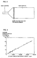
- Fig. 3 is a graph of carbon concentration in a GaAs crystal versus CO gas concentration in a LEC furnace found in Advanced Electronics Series I-4 Bulk Crystal Growth Technology , Keigo Hoshikawa, BAIFUKAN, p.184, Fig. 7.22.
- Fig. 3 shows that carbon concentration in a GaAs crystal end CO gas content in the LEC furnace are correlated by a straight line.
- the correlation represented in the graph is applied to the adjustment of carbon concentration in a GaAs crystal.
- the carbon concentration in a GaAs crystal can be controlled by adjusting the CO gas content in the ambient gas using a CO gas cylinder and an Ar gas cylinder for dilution connected to the stainless chamber.
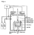
- Fig. 4 shows an exemplary GaAs crystal growth equipment for the LEC method disclosed in Japanese Patent Laying-Open No. 1-239089.
- Japanese Patent Laying-Open No. 1-239089 discloses a method of preparing a single crystal of compound semiconductor by placing in a predetermined gas ambient a raw-material housing portion housing a raw-material melt, detecting at least the concentration of one of H 2 , O 2 , CO 2 and CO corresponding to components of the ambient gas, and controlling the detected concentration of a component at a predetermined value to keep over the entirety of an ingot a predetermined concentration of a residual impurity mixed into a resulting single crystal.
- This method can, however, not be applied in preparing a compound semiconductor crystal in a gas-impermeable airtight vessel incapable of supplying a gas from outside the airtight vessel, such as a quartz ampoule.
- Japanese Patent Laying-Open No. 3-122097 discloses a method of preparing a GaAs crystal in a quartz ampoule wherein a carbon source is arranged internal to the ampoule and external to a crucible in fluid communication with a polycrystalline compound provided as a raw material to allow the GaAs crystal to be doped with carbon.
- Fluid communication means a free flow of vapor and heat between the inside and outside of the crucible which allows carbon to be transferred into the crucible and thus to a melt.
- a carbon disk is arranged on an opening of a cap. It discloses that the ingots of various doped levels can be provided by varying the amount of carbon arranged external to the opening and/or the crucible.
- Japanese Patent Laying-Open No. 64-79087 discloses a method of preparing a single crystal of GaAs doped with carbon to reduce dislocation, using a reactor or a boat for crystal growth at least partially formed of carbon. It discloses that when a graphite boat is used, a part of the carbon boat changes into a gas (CO or CO 2 ) due to oxygen derived from a small amount of As 2 O 3 , GA 2 O or the like remaining in the quartz reactor and the gas is thus added to the single crystal of GaAs in synthesis reaction or in single-crystal growth.
- a gas CO or CO 2
- Japanese Patent Laying-Open No. 2-48496 discloses a method of preparing a Cr-doped, semi-insulating GaAs crystal wherein a quartz boat or a quartz crucible is used to grow the crystal under the existence of nitrogen oxide or carbon oxide. It discloses that when a GaAs crystal is grown under the existence of nitrogen oxide or carbon oxide, the oxide serves as an oxygen doping source to reduce the Si concentration of the grown crystal so that a semi-insulating crystal is reliably provided.
- One object of the present invention is to provide a method of preparing a compound semiconductor crystal allowing the compound semiconductor crystal to be doped with carbon in high reproducibility, and a compound semiconductor crystal prepared thereby.
- a method of preparing a compound semiconductor crystal includes the steps of sealing carbon oxide gas of a predetermined partial pressure and a compound semiconductor provided as a raw material in a gas-impermeable airtight vessel, increasing the temperature of the airtight vessel to melt the compound semiconductor material sealed in the airtight vessel, decreasing the temperature of the airtight vessel to solidify the melt compound semiconductor material to grow a compound semiconductor crystal containing a predetermined amount of carbon.
- the carbon oxide gas includes at least one type of gas selected from the group consisting of CO gas and CO 2 gas.
- the melted compound semiconductor material is at least partially kept into contact with boron oxide (B 2 O 3 ).
- melt compound semiconductor material has its upper surface entirely covered with boron oxide (B 2 O 3 ).
- the boron oxide (B 2 O 3 ) has a water content of no more than 300 ppm, more preferably no more than 100 ppm.
- variation of the water content of the boron oxide (B 2 O 3 ) is controlled to fall within a range from +20% to -20%.
- the carbon oxide gas sealed in the airtight vessel preferably has a partial pressure of 0.1 to 100 Torr at 25°C.
- carbon oxide gas is preferably sealed in an airtight vessel according to an expression:
- C CARBON a ⁇ P 0.5
- C CARBON (cm ⁇ 3 ) represents carbon concentration in a compound semiconductor crystal
- P (Torr) represents partial pressure of the carbon oxide gas
- a represents any coefficient.
- coefficient a preferably ranges from 0.25 ⁇ 10 15 to 4 ⁇ 10 15 cm -3 /Torr, more preferably 0.5 ⁇ 10 15 to 2 ⁇ 10 15 cm -3 /Torr.
- the step of subjecting the airtight vessel to a vacuum heat treatment is also provided before the step of sealing carbon oxide gas in the airtight vessel.
- the vacuum heat treatment is preferably provided at a temperature of no more than 350°C.
- At least the internal wall of the airtight vessel and at least the outer surface of the contents of the airtight vessel other than the compound semiconductor material and the boron oxide are preferably formed from a material which does not contain carbon.
- the material which does not contain carbon includes at least one material selected from the group consisting, e.g., of quartz, silicon nitride, boron nitride, pyrolytic boron nitride and alumina.
- the gas-impermeable airtight vessel can at least partially be formed from quartz.
- the portion formed from quartz has a thickness of no less then 1.5 mm.
- the portion formed from quartz is controlled to have a temperature of at most 1270°C.
- a space behind a raw-material melt of melted compound preferably has its most heated portion and its least heated portion with a temperature difference of no more than 300°C therebetween.
- the space behind the raw-material melt is preferably larger, more preferably no less than twice larger in volume than the space on the side of the raw-material melt.
- a method of preparing a compound semiconductor crystal in accordance with the present invention is applicable to preparing a compound semiconductor crystal of GaAs.
- the piesent invention provides a compound semiconductor crystal prepared in accordance with the above-described method of preparing a compound semiconductor crystal, having a carbon concentration of 0.1 ⁇ 10 15 cm -3 to 20 ⁇ 10 15 cm -3 .
- the compound semiconductor includes GaAs.
- the present invention is based on a method of preparing a compound semiconductor crystal in a sealed system (a system incapable of supplying a gas from outside an airtight vessel) using a gas-impermeable airtight vessel.
- carbon oxide gas of a predetermined partial pressure as well as a compound semiconductor provided as a raw material are sealed in a gas-impermeable airtight vessel, the temperature of the airtight vessel is increased to melt the compound semiconductor material and the temperature of the airtight vessel is then decreased to solidify the melt compound semiconductor material to grow a compound semiconductor crystal to thereby allow the compound semiconductor crystal to be doped with carbon in high reproducibility.
- a stable CO or CO 2 gas can be used to allow the crystal to be doped with carbon in particularly high reproducibility.
- At least a portion of the melt of the compound semiconductor material can be kept into contact with boron oxide (B 2 O 3 ) and more preferably the upper surface of the melt can be entirely covered with boron oxide (B 2 O 3 ) to prevent other elements of impurities from being introduced into the melt so as to further enhance the reproducibility of the carbon concentration of the crystal.
- B 2 O 3 preferably has a water content of no more than 300 ppm, more preferably no more than 100 ppm.
- the variation of the water content of B 2 O 3 is preferably controlled to fall within a range from +20% to -20%.
- ambient gas is represented in concentration.
- an ambient gas for GaAs crystal growth typically has a pressure of 1 to 30 atm.
- the partial pressure of the latter is 30 times larger than that of the former.
- the inventors of the present invention have found that in a method of preparing a compound semiconductor crystal in a sealed system (a system incapable of supplying a gas from outside an airtight vessel) using a gas-impermeable airtight vessel, the carbon concentration in the crystal is correlated to the partial pressure of the carbon oxide gas sealed in the airtight vessel rather than the concentration of the carbon oxide gas sealed in the airtight vessel.
- the carbon oxide gas sealed in the airtight vessel is represented in the partial pressure at 25°C, since the partial pressure of the carbon oxide gas increases as the temperature of the airtight vessel is increased in growing a crystal. Since a GaAs crystal has a melting point of approximately 1238°C, the partial pressure of the carbon oxide gas sealed at a room temperature (of 25°C) is considered to be increased by approximately five times during the crystal growth.
- carbon oxide gas having a predetermined partial pressure is sealed in an airtight vessel
- carbon oxide gas may be sealed together with another gas, which can include inert gases, such as helium, neon, argon, krypton, xenon, and nitride gas.
- inert gases such as helium, neon, argon, krypton, xenon, and nitride gas.
- carbon oxide gas When carbon oxide gas is only sealed, it has a concentration of 100%.
- carbon oxide gas is sealed, e.g., together with any of the above gases of 50%, the carbon oxide gas has a concentration of 50%.
- Removal of water absorbed in the airtight vessel further enhance the reproducibility of the carbon concentration in the crystal. Accordingly it is preferable to apply a vacuum heat treatment to the airtight vessel before it is sealed.
- the vacuum heat treatment applied immediately before the vessel is sealed is applied preferably at no more than 350°C, at which temperature B 2 O 3 does not soften or deform.
- At least the internal wall of the airtight vessel and at least the outer surface of the contents of the vessel other than the compound semiconductor as a raw material and boron oxide are preferably formed from a material which does not contain carbon, so that further generation of carbon oxide gas can be prevented in the vessel.
- the airtight vessel is preferably formed from a material which does not contain carbon, or the vessel preferably has its internal wall coated with a material which does not contain carbon.
- the contents of the airtight vessel other than the compound semiconductor material and boron oxide be formed from a material which does not contain carbon or that the contents have the outer surface coated with a material which does not contain carbon.
- the material which does not contain carbon is preferably quartz, silicon nitride, boron nitride, pyrolytic boron nitride or alumina.
- the gas-impermeable airtight vessel of the present invention can at least partially be formed from quartz, since quartz has superior airtightness and hardly reacts with elements forming the compound semiconductor or carbon oxide gas.
- carbon oxide gas having a predetermined partial pressure is sealed in a gas-impermeable airtight vessel.
- the airtight vessel is deformed and its internal volume is changed, the partial pressure of the sealed carbon oxide gas is changed and the carbon concentration of the resulting compound semiconductor crystal will deviate from a targeted carbon concentration.
- the strength of quartz is reduced at high temperature and is significantly reduced at a temperature at which a GaAs crystal is grown, i.e., 1238°C.
- a gas-impermeable airtight vessel is at least partially formed from quartz, the difference between the pressure internal to the vessel and that external to the vessel deforms the quartz portion of the vessel and thus changes the internal volume of the vessel.
- the inventors of the present invention have found that as the vessel's quartz portion is increased in thickness, deformation of the quartz portion is reduced at high temperatures and variation in the vessel's internal volume is thus reduced.
- the quartz portion of the vessel preferably has a thickness of no less than 1.5 mm, more preferably no less than 2.0 mm, still more preferably no less than 2.5 mm.
- the inventors have also found that as temperature is decreased, deformation of quartz is reduced and variation in the vessel's internal volume is reduced.
- the quartz portion of the vessel preferably has a temperature of at most 1270°C, more preferably at most 1260°C, further still more preferably at most 1250°C.
- carbon oxide gas of a predetermined partial pressure is sealed in a gas-impermeable airtight vessel.
- the partial pressure of the sealed carbon oxide gas changes and the carbon concentration of the resulting compound semiconductor crystal thus deviates from a targeted carbon concentration.
- the space on the side of the raw-material melt more specifically, the space located below the interface (labeled A in Fig. 1) of raw-material melt 2 and boron oxide 4, i.e., the space on the side of the seed crystal has its temperature reduced as crystal growth proceeds.
- the space on the side of the raw-material melt is large in volume, the average temperature and hence partial pressure of the carbon oxide gas in the airtight vessel are reduced significantly.
- the temperature of the space behind the raw-material melt i.e., that located above interface A can be controlled regardless of crystal growth.
- controlling the temperature of the space behind the raw-material melt can prevent reduction of the average temperature of the carbon oxide gas in the airtight vessel and reduce reduction of the partial pressure of the carbon oxide gas in the vessel.
- Reducing the temperature difference between the most and least heated portions of the space behind the raw-material melt can reduce reduction of the partial pressure of the carbon oxide gas in the vessel.
- the temperature difference between the most and least heated potions of the space behind the melt is preferably no more than 300°C, more preferably no more than 200°C, still more preferably no more than 100°C.
- the space behind the raw-material melt that is larger in volume than the space on the side of the raw-material melt can further reduce the reduction of the partial pressure of the carbon oxide gas in the vessel that is caused when the average temperature of the gas in the vessel is reduced.
- the space behind the raw-material melt is preferably no less than twice, more preferably no less than three times, still more preferably no less than four times larger in volume than that on the side of the raw-materil melt.
- the method of the present invention is particularly applicable to preparation of GaAs crystal.
- Fig. 1 shows an exemplary method of preparing a compound semiconductor crystal in accordance with the present invention, using a gas-impermeable airtight vessel formed from quartz (referred to as a "quartz ampoule” hereinafter) to prepare a GaAs crystal.
- a gas-impermeable airtight vessel formed from quartz referred to as a "quartz ampoule” hereinafter
- a GaAs seed crystal 3 of orientation (100), 5 kg of GaAs 2 as a raw material, and 50 g of boron oxide 4 (referred to as “B 2 O 3 " hereinafter) with a water content of 70 ppm were initially placed in a crucible 5 formed from pyrolytic boron nitride (referred to as "pBN" hereinafter) and having an inner diameter of 80 mm and also having a cylindrical portion of approximately 30 cm in length, and crucible 5 was housed in a quartz ampoule 8 of 2.5 mm thick.
- the space behind the raw-material melt placed in quartz ampoule 8, i.e., that located above the interface denoted by arrow A in Fig. 1 was adapted to be four times larger in volume than the space on the side of the raw-material melt, i.e., that located below interface A).
- Quartz ampoule 8 was vacuumed to 1 ⁇ 10 -6 Torr and also heated to 300°C to remove water adsorbed on the internal wall of ampoule 8 and the raw material. Then, CO 2 gas 7 of 3 Torr was introduced and sealed in ampoule 8. Ampoule 8 was mounted on a support 9 and thus set internal to a vertical beater 6 provided in a chamber 10, and the temperature of beater 6 was increased to melt GaAs material 2 and an upper portion of seed crystal 3.
- the temperature profile of the beater was adjusted to decrease the temperature from the side of the seed crystal 3 and the entirety of raw-material melt 2 was thus solidified to grow a crystal.
- the highest temperature of ampoule 8 was also controlled not to exceed 1250°.
- the temperature of an upper portion of ampoule 8 was controlled so that the space located behind the raw-material melt, i.e., that located above interface A shown in Fig. 1 had its most heated portion and its least heated portion with a temperature difference of no more than 100°C therebetween.
- the temperature was reduced to a room temperature and quartz ampoule 8 was then cut and opened to separate a GaAs crystal from crucible 5.
- the resulting GaAs crystal had a diameter of 80 mm, and the portion having the diameter of 80 mm was approximately 18 cm long.
- a sample of 5 mm thick for measurement of carbon concentration was cut out at the position of a shoulder of the crystal (fraction solidified: g of 0.1).
- Fig. 2 shows the position of the shoulder of the crystal from which the sample was cut out.
- Fourier Transform Infrared Spectroscopy was used to measure the concentration of the carbon substituted at an arsenic site (referred to as "C As " hereinafter). The measured C As concentration was 2.1 ⁇ 10 15 cm -3 .
- the present invention can provide a method of preparing a compound semiconductor crystal in a sealed system (a system incapable of supplying a gas from outside an airtight vessel) using a gas-impermeable airtight vessel to allow the compound semiconductor crystal to be doped with carbon in high reproducibility.
- carbon oxide gas of a predetermined partial pressure sealed in the gas-impermeable airtight vessel together with compound semiconductor provided as a raw material allows a compound semiconductor crystal with a desired carbon concentration and hence with a desired electrical characteristic to be prepared in high reproducibility, since the electrical characteristic of the compound semiconductor crystal depends on the carbon concentration of the crystal.
- the present invention can provide satisfactory crystal yield.
Landscapes
- Chemical & Material Sciences (AREA)
- Engineering & Computer Science (AREA)
- Crystallography & Structural Chemistry (AREA)
- Materials Engineering (AREA)
- Metallurgy (AREA)
- Organic Chemistry (AREA)
- Inorganic Chemistry (AREA)
- Crystals, And After-Treatments Of Crystals (AREA)
- Liquid Deposition Of Substances Of Which Semiconductor Devices Are Composed (AREA)
Priority Applications (1)
| Application Number | Priority Date | Filing Date | Title |
|---|---|---|---|
| EP04003550.3A EP1428912B1 (fr) | 1998-03-25 | 1999-03-23 | Procédé pour la préparation d'un cristal d'un composé semi-conducteur comprenant du carbon |
Applications Claiming Priority (2)
| Application Number | Priority Date | Filing Date | Title |
|---|---|---|---|
| JP7730998 | 1998-03-25 | ||
| JP7730998 | 1998-03-25 |
Related Child Applications (1)
| Application Number | Title | Priority Date | Filing Date |
|---|---|---|---|
| EP04003550.3A Division EP1428912B1 (fr) | 1998-03-25 | 1999-03-23 | Procédé pour la préparation d'un cristal d'un composé semi-conducteur comprenant du carbon |
Publications (3)
| Publication Number | Publication Date |
|---|---|
| EP0947609A2 true EP0947609A2 (fr) | 1999-10-06 |
| EP0947609A3 EP0947609A3 (fr) | 2002-02-06 |
| EP0947609B1 EP0947609B1 (fr) | 2004-02-18 |
Family
ID=13630320
Family Applications (2)
| Application Number | Title | Priority Date | Filing Date |
|---|---|---|---|
| EP99105861A Expired - Lifetime EP0947609B1 (fr) | 1998-03-25 | 1999-03-23 | Cristal d'un semi-conducteur du type composé et procédé pour sa préparation |
| EP04003550.3A Expired - Lifetime EP1428912B1 (fr) | 1998-03-25 | 1999-03-23 | Procédé pour la préparation d'un cristal d'un composé semi-conducteur comprenant du carbon |
Family Applications After (1)
| Application Number | Title | Priority Date | Filing Date |
|---|---|---|---|
| EP04003550.3A Expired - Lifetime EP1428912B1 (fr) | 1998-03-25 | 1999-03-23 | Procédé pour la préparation d'un cristal d'un composé semi-conducteur comprenant du carbon |
Country Status (4)
| Country | Link |
|---|---|
| US (4) | US6273947B1 (fr) |
| EP (2) | EP0947609B1 (fr) |
| JP (2) | JP3596337B2 (fr) |
| DE (1) | DE69914820T2 (fr) |
Cited By (1)
| Publication number | Priority date | Publication date | Assignee | Title |
|---|---|---|---|---|
| EP2444531A3 (fr) * | 2001-07-05 | 2012-10-31 | Axt, Inc. | Procédé et appareil de croissance de cristaux semi-conducteurs avec support rigide et avec dopage de carbone |
Families Citing this family (8)
| Publication number | Priority date | Publication date | Assignee | Title |
|---|---|---|---|---|
| JP3596337B2 (ja) * | 1998-03-25 | 2004-12-02 | 住友電気工業株式会社 | 化合物半導体結晶の製造方法 |
| JP5186733B2 (ja) * | 2005-07-29 | 2013-04-24 | 住友電気工業株式会社 | AlN結晶の成長方法 |
| US20080264332A1 (en) * | 2007-04-25 | 2008-10-30 | Fareed Sepehry-Fard | Method, system, and apparatus for doping and for multi-chamber high-throughput solid-phase epitaxy deposition process |
| US8361225B2 (en) | 2007-05-09 | 2013-01-29 | Axt, Inc. | Low etch pit density (EPD) semi-insulating III-V wafers |
| US7566641B2 (en) * | 2007-05-09 | 2009-07-28 | Axt, Inc. | Low etch pit density (EPD) semi-insulating GaAs wafers |
| EP2072645B2 (fr) * | 2007-12-19 | 2014-12-24 | Schott AG | Procédé de production d'un matériau semi-conducteur monocristallin ou polycristallin |
| JP5110026B2 (ja) * | 2009-04-03 | 2012-12-26 | 住友電気工業株式会社 | Iii−v族化合物半導体結晶の製造方法 |
| JP6411952B2 (ja) | 2015-06-09 | 2018-10-24 | 信越化学工業株式会社 | 熱分解窒化ほう素容器の製造方法 |
Family Cites Families (42)
| Publication number | Priority date | Publication date | Assignee | Title |
|---|---|---|---|---|
| US4083748A (en) | 1975-10-30 | 1978-04-11 | Western Electric Company, Inc. | Method of forming and growing a single crystal of a semiconductor compound |
| US4521272A (en) | 1981-01-05 | 1985-06-04 | At&T Technologies, Inc. | Method for forming and growing a single crystal of a semiconductor compound |
| US4404172A (en) | 1981-01-05 | 1983-09-13 | Western Electric Company, Inc. | Method and apparatus for forming and growing a single crystal of a semiconductor compound |
| JPS5914440B2 (ja) | 1981-09-18 | 1984-04-04 | 住友電気工業株式会社 | CaAs単結晶への硼素のド−ピング方法 |
| JPS5954699A (ja) | 1982-09-22 | 1984-03-29 | Toshiba Corp | 単結晶の製造方法 |
| JP2529934B2 (ja) | 1984-02-21 | 1996-09-04 | 住友電気工業株式会社 | 単結晶の製造方法 |
| US5256381A (en) | 1984-02-21 | 1993-10-26 | Sumitomo Electric Industries, Ltd. | Apparatus for growing single crystals of III-V compound semiconductors |
| JPS60210599A (ja) * | 1984-04-03 | 1985-10-23 | Nec Corp | 半絶縁性GaAs結晶の成長方法 |
| JPS60264390A (ja) | 1984-06-08 | 1985-12-27 | Sumitomo Electric Ind Ltd | 単結晶の育成方法 |
| JPS6437833A (en) * | 1987-08-03 | 1989-02-08 | Nippon Mining Co | Semi-insulating gaas single crystal |
| JPS6437833U (fr) | 1987-09-01 | 1989-03-07 | ||
| JPS6479087A (en) | 1987-09-21 | 1989-03-24 | Hitachi Cable | Gallium arsenide single crystal having low dislocation density and its production |
| JPH01239089A (ja) | 1987-11-30 | 1989-09-25 | Toshiba Corp | 化合物半導体単結晶の製造方法及び製造装置 |
| JPH0234597A (ja) * | 1988-07-26 | 1990-02-05 | Sumitomo Electric Ind Ltd | 水平ブリッジマン法によるGaAs単結晶の成長方法 |
| JPH0772120B2 (ja) | 1988-08-05 | 1995-08-02 | 日立電線株式会社 | Crドープ半絶縁性砒化ガリウム結晶の製造方法 |
| JPH08758B2 (ja) | 1988-09-08 | 1996-01-10 | 日立電線株式会社 | クロムドープ半絶縁性ガリウム・ヒ素単結晶の製造方法 |
| US4923561A (en) | 1988-09-23 | 1990-05-08 | American Telephone And Telegraph Company | Crystal growth method |
| US5057287A (en) * | 1988-11-01 | 1991-10-15 | Sfa, Inc. | Liquid encapsulated zone melting crystal growth method and apparatus |
| JP3122097B2 (ja) | 1988-12-20 | 2001-01-09 | 富士通株式会社 | 文書読み上げ制御装置および文書読み上げ方法 |
| US4946544A (en) | 1989-02-27 | 1990-08-07 | At&T Bell Laboratories | Crystal growth method |
| US5259916A (en) | 1989-06-20 | 1993-11-09 | Texas Instruments Incorporated | Process for improved doping of semiconductor crystals |
| US5186784A (en) | 1989-06-20 | 1993-02-16 | Texas Instruments Incorporated | Process for improved doping of semiconductor crystals |
| US4999082A (en) | 1989-09-14 | 1991-03-12 | Akzo America Inc. | Process for producing monocrystalline group II-IV or group III-V compounds and products thereof |
| US5131975A (en) | 1990-07-10 | 1992-07-21 | The Regents Of The University Of California | Controlled growth of semiconductor crystals |
| JPH04104989A (ja) | 1990-08-25 | 1992-04-07 | Sumitomo Electric Ind Ltd | 液相エピタキシャル成長方法および装置 |
| US5342475A (en) | 1991-06-07 | 1994-08-30 | The Furukawa Electric Co., Ltd. | Method of growing single crystal of compound semiconductor |
| DE69233617D1 (de) | 1991-08-22 | 2006-05-24 | Raytheon Co | Verfahren zum Entfernen einer B2O3-Einkapselungsmasse von einer Struktur |
| JPH0570288A (ja) | 1991-09-09 | 1993-03-23 | Toshiba Corp | 化合物半導体単結晶の製造方法及び製造装置 |
| JPH05139886A (ja) | 1991-11-21 | 1993-06-08 | Toshiba Corp | 砒素化合物単結晶の製造方法 |
| JP2781097B2 (ja) | 1992-01-30 | 1998-07-30 | 三菱電機株式会社 | 半導体装置およびその製造方法 |
| JPH06128096A (ja) | 1992-10-20 | 1994-05-10 | Furukawa Electric Co Ltd:The | 化合物半導体多結晶の製造方法 |
| JPH06239691A (ja) | 1993-02-12 | 1994-08-30 | Japan Energy Corp | 単結晶の成長方法 |
| JP3015656B2 (ja) * | 1994-03-23 | 2000-03-06 | 株式会社東芝 | 半絶縁性GaAs単結晶の製造方法および製造装置 |
| WO1995033873A1 (fr) * | 1994-06-02 | 1995-12-14 | Kabushiki Kaisha Kobe Seiko Sho | Procede et dispositif de production d'un monocristal macle |
| JPH0930887A (ja) | 1995-07-17 | 1997-02-04 | Hitachi Cable Ltd | 炭素添加GaAs結晶の製造方法 |
| JP3201305B2 (ja) * | 1996-04-26 | 2001-08-20 | 住友電気工業株式会社 | Iii−v族化合物半導体結晶の製造方法 |
| JPH09309791A (ja) * | 1996-05-22 | 1997-12-02 | Komatsu Electron Metals Co Ltd | 半導体単結晶の製造方法 |
| JP4120016B2 (ja) | 1996-12-12 | 2008-07-16 | 住友電気工業株式会社 | 半絶縁性GaAs単結晶の製造方法 |
| JP3969865B2 (ja) | 1997-10-24 | 2007-09-05 | キヤノン株式会社 | フッ化物結晶の製造方法 |
| JPH11147785A (ja) | 1997-11-11 | 1999-06-02 | Hitachi Cable Ltd | 単結晶の製造方法 |
| JP4135239B2 (ja) * | 1997-12-26 | 2008-08-20 | 住友電気工業株式会社 | 半導体結晶およびその製造方法ならびに製造装置 |
| JP3596337B2 (ja) * | 1998-03-25 | 2004-12-02 | 住友電気工業株式会社 | 化合物半導体結晶の製造方法 |
-
1999
- 1999-03-10 JP JP6314399A patent/JP3596337B2/ja not_active Expired - Lifetime
- 1999-03-22 US US09/274,286 patent/US6273947B1/en not_active Expired - Lifetime
- 1999-03-23 DE DE69914820T patent/DE69914820T2/de not_active Expired - Lifetime
- 1999-03-23 EP EP99105861A patent/EP0947609B1/fr not_active Expired - Lifetime
- 1999-03-23 EP EP04003550.3A patent/EP1428912B1/fr not_active Expired - Lifetime
-
2001
- 2001-01-19 US US09/765,557 patent/US6485563B2/en not_active Ceased
-
2003
- 2003-08-13 US US10/640,430 patent/USRE40662E1/en not_active Expired - Lifetime
-
2004
- 2004-06-15 JP JP2004177249A patent/JP4096919B2/ja not_active Expired - Lifetime
-
2008
- 2008-12-22 US US12/341,876 patent/USRE42279E1/en not_active Expired - Lifetime
Cited By (2)
| Publication number | Priority date | Publication date | Assignee | Title |
|---|---|---|---|---|
| EP2444531A3 (fr) * | 2001-07-05 | 2012-10-31 | Axt, Inc. | Procédé et appareil de croissance de cristaux semi-conducteurs avec support rigide et avec dopage de carbone |
| CN102797032A (zh) * | 2001-07-05 | 2012-11-28 | Axt公司 | 具有坚固支撑、碳掺杂、电阻率控制和热梯度控制的半导体晶体生长的方法和装置 |
Also Published As
| Publication number | Publication date |
|---|---|
| EP1428912A2 (fr) | 2004-06-16 |
| JP2004256392A (ja) | 2004-09-16 |
| JP3596337B2 (ja) | 2004-12-02 |
| DE69914820T2 (de) | 2004-07-29 |
| JP4096919B2 (ja) | 2008-06-04 |
| EP0947609B1 (fr) | 2004-02-18 |
| USRE42279E1 (en) | 2011-04-12 |
| US6273947B1 (en) | 2001-08-14 |
| US20010006040A1 (en) | 2001-07-05 |
| EP1428912B1 (fr) | 2014-11-05 |
| DE69914820D1 (de) | 2004-03-25 |
| EP1428912A9 (fr) | 2004-09-08 |
| JPH11335195A (ja) | 1999-12-07 |
| EP0947609A3 (fr) | 2002-02-06 |
| USRE40662E1 (en) | 2009-03-17 |
| EP1428912A3 (fr) | 2004-06-23 |
| US6485563B2 (en) | 2002-11-26 |
Similar Documents
| Publication | Publication Date | Title |
|---|---|---|
| USRE42279E1 (en) | Method of preparing a compound semiconductor crystal | |
| US5515810A (en) | Method and apparatus for manufacturing semi-insulation GaAs monocrystal | |
| US7279040B1 (en) | Method and apparatus for zinc oxide single crystal boule growth | |
| US6007622A (en) | Method of preparing group III-V compound semiconductor crystal | |
| US6773505B2 (en) | Method for the sublimation growth of an SiC single crystal, involving heating under growth pressure | |
| US5041186A (en) | Method for manufacturing compound semiconductor single crystals using a hydrogen monitor gas | |
| JP4135239B2 (ja) | 半導体結晶およびその製造方法ならびに製造装置 | |
| JP4416040B2 (ja) | 化合物半導体結晶 | |
| Shinoyama et al. | Growth of dislocation-free undoped InP crystals | |
| JP4120016B2 (ja) | 半絶縁性GaAs単結晶の製造方法 | |
| EP2390386B1 (fr) | Procédé et appareil de production de cristal semi-conducteur au nitrure | |
| EP0559921B1 (fr) | Appareil et procede de production d'un semiconducteur monocristallin d'un compose a pression elevee de dissociation | |
| JPH06298600A (ja) | SiC単結晶の成長方法 | |
| JPS63107886A (ja) | 雰囲気ガス制御による結晶製造方法 | |
| JP4400304B2 (ja) | Iii−v族化合物半導体結晶の製造方法 | |
| JPS63265897A (ja) | 3−5族化合物半導体単結晶の製造装置 | |
| JP3551607B2 (ja) | GaAs単結晶の製造方法 | |
| Glass et al. | Control of Defects and Impurities in Production of CdZnTe Crystals by the Bridgman Method | |
| JPH07187886A (ja) | 半絶縁性GaAs単結晶の製造方法及び製造装置 | |
| JP2001080989A (ja) | 化合物半導体単結晶の製造装置及びそれを用いた製造方法 | |
| JPH089517B2 (ja) | 単結晶製造方法 | |
| JPH1112087A (ja) | 化合物半導体単結晶の製造方法 | |
| JPH08253396A (ja) | GaAs単結晶の成長方法 | |
| JPS63242988A (ja) | 3−5族化合物半導体の単結晶製造装置 | |
| JPH02243596A (ja) | 化合物半導体単結晶製造装置 |
Legal Events
| Date | Code | Title | Description |
|---|---|---|---|
| PUAI | Public reference made under article 153(3) epc to a published international application that has entered the european phase |
Free format text: ORIGINAL CODE: 0009012 |
|
| AK | Designated contracting states |
Kind code of ref document: A2 Designated state(s): AT BE CH CY DE DK ES FI FR GB GR IE IT LI LU MC NL PT SE Kind code of ref document: A2 Designated state(s): DE FR GB |
|
| AX | Request for extension of the european patent |
Free format text: AL;LT;LV;MK;RO;SI |
|
| PUAL | Search report despatched |
Free format text: ORIGINAL CODE: 0009013 |
|
| AK | Designated contracting states |
Kind code of ref document: A3 Designated state(s): AT BE CH CY DE DK ES FI FR GB GR IE IT LI LU MC NL PT SE |
|
| AX | Request for extension of the european patent |
Free format text: AL;LT;LV;MK;RO;SI |
|
| RIC1 | Information provided on ipc code assigned before grant |
Free format text: 7C 30B 29/42 A, 7C 30B 27/00 B, 7C 30B 11/12 B, 7C 30B 11/00 B |
|
| 17P | Request for examination filed |
Effective date: 20020121 |
|
| 17Q | First examination report despatched |
Effective date: 20020326 |
|
| AKX | Designation fees paid |
Free format text: DE FR GB |
|
| GRAP | Despatch of communication of intention to grant a patent |
Free format text: ORIGINAL CODE: EPIDOSNIGR1 |
|
| GRAS | Grant fee paid |
Free format text: ORIGINAL CODE: EPIDOSNIGR3 |
|
| GRAA | (expected) grant |
Free format text: ORIGINAL CODE: 0009210 |
|
| AK | Designated contracting states |
Kind code of ref document: B1 Designated state(s): DE FR GB |
|
| REG | Reference to a national code |
Ref country code: GB Ref legal event code: FG4D |
|
| REG | Reference to a national code |
Ref country code: IE Ref legal event code: FG4D |
|
| REF | Corresponds to: |
Ref document number: 69914820 Country of ref document: DE Date of ref document: 20040325 Kind code of ref document: P |
|
| ET | Fr: translation filed | ||
| PLBQ | Unpublished change to opponent data |
Free format text: ORIGINAL CODE: EPIDOS OPPO |
|
| PLBI | Opposition filed |
Free format text: ORIGINAL CODE: 0009260 |
|
| PLAX | Notice of opposition and request to file observation + time limit sent |
Free format text: ORIGINAL CODE: EPIDOSNOBS2 |
|
| 26 | Opposition filed |
Opponent name: FREIBERGER COMPOUND MATERIALS GMBH Effective date: 20041117 |
|
| REG | Reference to a national code |
Ref country code: IE Ref legal event code: MM4A |
|
| PLBB | Reply of patent proprietor to notice(s) of opposition received |
Free format text: ORIGINAL CODE: EPIDOSNOBS3 |
|
| PLBP | Opposition withdrawn |
Free format text: ORIGINAL CODE: 0009264 |
|
| PLBD | Termination of opposition procedure: decision despatched |
Free format text: ORIGINAL CODE: EPIDOSNOPC1 |
|
| PLBM | Termination of opposition procedure: date of legal effect published |
Free format text: ORIGINAL CODE: 0009276 |
|
| STAA | Information on the status of an ep patent application or granted ep patent |
Free format text: STATUS: OPPOSITION PROCEDURE CLOSED |
|
| 27C | Opposition proceedings terminated |
Effective date: 20050922 |
|
| REG | Reference to a national code |
Ref country code: FR Ref legal event code: PLFP Year of fee payment: 18 |
|
| REG | Reference to a national code |
Ref country code: FR Ref legal event code: PLFP Year of fee payment: 19 |
|
| REG | Reference to a national code |
Ref country code: FR Ref legal event code: PLFP Year of fee payment: 20 |
|
| PGFP | Annual fee paid to national office [announced via postgrant information from national office to epo] |
Ref country code: DE Payment date: 20180313 Year of fee payment: 20 Ref country code: GB Payment date: 20180321 Year of fee payment: 20 |
|
| PGFP | Annual fee paid to national office [announced via postgrant information from national office to epo] |
Ref country code: FR Payment date: 20180223 Year of fee payment: 20 |
|
| REG | Reference to a national code |
Ref country code: DE Ref legal event code: R071 Ref document number: 69914820 Country of ref document: DE |
|
| REG | Reference to a national code |
Ref country code: GB Ref legal event code: PE20 Expiry date: 20190322 |
|
| PG25 | Lapsed in a contracting state [announced via postgrant information from national office to epo] |
Ref country code: GB Free format text: LAPSE BECAUSE OF EXPIRATION OF PROTECTION Effective date: 20190322 |