EP0948022A2 - Verfahren und Vorrichtung zur Herstellung einer Elektronenquelle und Herstellungsverfahren eines Bilderzeugungsgeräts - Google Patents
Verfahren und Vorrichtung zur Herstellung einer Elektronenquelle und Herstellungsverfahren eines Bilderzeugungsgeräts Download PDFInfo
- Publication number
- EP0948022A2 EP0948022A2 EP99302486A EP99302486A EP0948022A2 EP 0948022 A2 EP0948022 A2 EP 0948022A2 EP 99302486 A EP99302486 A EP 99302486A EP 99302486 A EP99302486 A EP 99302486A EP 0948022 A2 EP0948022 A2 EP 0948022A2
- Authority
- EP
- European Patent Office
- Prior art keywords
- potential
- wiring
- activation
- circuit
- current
- Prior art date
- Legal status (The legal status is an assumption and is not a legal conclusion. Google has not performed a legal analysis and makes no representation as to the accuracy of the status listed.)
- Withdrawn
Links
- 238000004519 manufacturing process Methods 0.000 title claims abstract description 56
- 238000000034 method Methods 0.000 title claims description 86
- 238000009826 distribution Methods 0.000 claims description 192
- 238000012544 monitoring process Methods 0.000 claims description 53
- 239000011159 matrix material Substances 0.000 claims description 34
- 230000008859 change Effects 0.000 claims description 29
- 238000012358 sourcing Methods 0.000 claims 1
- 230000004913 activation Effects 0.000 description 323
- 239000000758 substrate Substances 0.000 description 86
- 238000012545 processing Methods 0.000 description 72
- 239000010409 thin film Substances 0.000 description 50
- 239000010408 film Substances 0.000 description 48
- 238000010894 electron beam technology Methods 0.000 description 38
- 239000000463 material Substances 0.000 description 24
- 239000010419 fine particle Substances 0.000 description 22
- 238000010586 diagram Methods 0.000 description 21
- OKTJSMMVPCPJKN-UHFFFAOYSA-N Carbon Chemical compound [C] OKTJSMMVPCPJKN-UHFFFAOYSA-N 0.000 description 14
- 229910052751 metal Inorganic materials 0.000 description 14
- 239000002184 metal Substances 0.000 description 14
- 239000000126 substance Substances 0.000 description 12
- 238000012937 correction Methods 0.000 description 11
- 230000003213 activating effect Effects 0.000 description 10
- 238000005259 measurement Methods 0.000 description 8
- 150000002894 organic compounds Chemical class 0.000 description 8
- 238000012546 transfer Methods 0.000 description 8
- 238000004364 calculation method Methods 0.000 description 7
- 229910052799 carbon Inorganic materials 0.000 description 7
- 230000007423 decrease Effects 0.000 description 7
- 238000001514 detection method Methods 0.000 description 7
- 229910002804 graphite Inorganic materials 0.000 description 7
- 239000010439 graphite Substances 0.000 description 7
- XOLBLPGZBRYERU-UHFFFAOYSA-N tin dioxide Chemical compound O=[Sn]=O XOLBLPGZBRYERU-UHFFFAOYSA-N 0.000 description 7
- 150000001722 carbon compounds Chemical class 0.000 description 6
- 238000013461 design Methods 0.000 description 6
- 239000002245 particle Substances 0.000 description 6
- 230000002093 peripheral effect Effects 0.000 description 6
- 239000002904 solvent Substances 0.000 description 6
- VYPSYNLAJGMNEJ-UHFFFAOYSA-N Silicium dioxide Chemical compound O=[Si]=O VYPSYNLAJGMNEJ-UHFFFAOYSA-N 0.000 description 5
- 239000012298 atmosphere Substances 0.000 description 5
- 230000004044 response Effects 0.000 description 5
- 238000000151 deposition Methods 0.000 description 4
- 238000005530 etching Methods 0.000 description 4
- 238000004544 sputter deposition Methods 0.000 description 4
- 101100219189 Caenorhabditis elegans byn-1 gene Proteins 0.000 description 3
- -1 In2O3-SnO2 Chemical class 0.000 description 3
- 229910003481 amorphous carbon Inorganic materials 0.000 description 3
- 230000015572 biosynthetic process Effects 0.000 description 3
- 230000000694 effects Effects 0.000 description 3
- 238000000605 extraction Methods 0.000 description 3
- 238000010438 heat treatment Methods 0.000 description 3
- 150000002739 metals Chemical class 0.000 description 3
- 239000000203 mixture Substances 0.000 description 3
- 238000000206 photolithography Methods 0.000 description 3
- 238000001771 vacuum deposition Methods 0.000 description 3
- 101100010712 Caenorhabditis elegans dyn-1 gene Proteins 0.000 description 2
- 229910002674 PdO Inorganic materials 0.000 description 2
- 229910052804 chromium Inorganic materials 0.000 description 2
- 229910052681 coesite Inorganic materials 0.000 description 2
- 229910052802 copper Inorganic materials 0.000 description 2
- 229910052906 cristobalite Inorganic materials 0.000 description 2
- 238000001704 evaporation Methods 0.000 description 2
- 230000001747 exhibiting effect Effects 0.000 description 2
- 239000011521 glass Substances 0.000 description 2
- PJXISJQVUVHSOJ-UHFFFAOYSA-N indium(III) oxide Inorganic materials [O-2].[O-2].[O-2].[In+3].[In+3] PJXISJQVUVHSOJ-UHFFFAOYSA-N 0.000 description 2
- 229910044991 metal oxide Inorganic materials 0.000 description 2
- 150000004706 metal oxides Chemical class 0.000 description 2
- 229910052763 palladium Inorganic materials 0.000 description 2
- 238000000059 patterning Methods 0.000 description 2
- 229910052697 platinum Inorganic materials 0.000 description 2
- 238000007639 printing Methods 0.000 description 2
- 239000000377 silicon dioxide Substances 0.000 description 2
- 239000005361 soda-lime glass Substances 0.000 description 2
- 229910052682 stishovite Inorganic materials 0.000 description 2
- 229910052718 tin Inorganic materials 0.000 description 2
- 229910052719 titanium Inorganic materials 0.000 description 2
- 229910052905 tridymite Inorganic materials 0.000 description 2
- 229910052721 tungsten Inorganic materials 0.000 description 2
- 229910003862 HfB2 Inorganic materials 0.000 description 1
- 229910025794 LaB6 Inorganic materials 0.000 description 1
- ATJFFYVFTNAWJD-UHFFFAOYSA-N Tin Chemical compound [Sn] ATJFFYVFTNAWJD-UHFFFAOYSA-N 0.000 description 1
- 229910007948 ZrB2 Inorganic materials 0.000 description 1
- 238000009825 accumulation Methods 0.000 description 1
- 229910045601 alloy Inorganic materials 0.000 description 1
- 239000000956 alloy Substances 0.000 description 1
- PNEYBMLMFCGWSK-UHFFFAOYSA-N aluminium oxide Inorganic materials [O-2].[O-2].[O-2].[Al+3].[Al+3] PNEYBMLMFCGWSK-UHFFFAOYSA-N 0.000 description 1
- GHPGOEFPKIHBNM-UHFFFAOYSA-N antimony(3+);oxygen(2-) Chemical compound [O-2].[O-2].[O-2].[Sb+3].[Sb+3] GHPGOEFPKIHBNM-UHFFFAOYSA-N 0.000 description 1
- 238000003491 array Methods 0.000 description 1
- VWZIXVXBCBBRGP-UHFFFAOYSA-N boron;zirconium Chemical compound B#[Zr]#B VWZIXVXBCBBRGP-UHFFFAOYSA-N 0.000 description 1
- 230000015556 catabolic process Effects 0.000 description 1
- 239000000919 ceramic Substances 0.000 description 1
- 239000003086 colorant Substances 0.000 description 1
- 239000004020 conductor Substances 0.000 description 1
- 239000000470 constituent Substances 0.000 description 1
- 238000010276 construction Methods 0.000 description 1
- 230000003247 decreasing effect Effects 0.000 description 1
- 238000006731 degradation reaction Methods 0.000 description 1
- 239000003599 detergent Substances 0.000 description 1
- 238000007598 dipping method Methods 0.000 description 1
- 238000010292 electrical insulation Methods 0.000 description 1
- 238000009429 electrical wiring Methods 0.000 description 1
- 239000012777 electrically insulating material Substances 0.000 description 1
- 230000005611 electricity Effects 0.000 description 1
- 239000007772 electrode material Substances 0.000 description 1
- 230000008020 evaporation Effects 0.000 description 1
- 229910052737 gold Inorganic materials 0.000 description 1
- 238000009499 grossing Methods 0.000 description 1
- 230000006872 improvement Effects 0.000 description 1
- 229910052738 indium Inorganic materials 0.000 description 1
- 238000003780 insertion Methods 0.000 description 1
- 230000037431 insertion Effects 0.000 description 1
- 239000012212 insulator Substances 0.000 description 1
- 150000002500 ions Chemical class 0.000 description 1
- 229910052742 iron Inorganic materials 0.000 description 1
- 229910052745 lead Inorganic materials 0.000 description 1
- YEXPOXQUZXUXJW-UHFFFAOYSA-N lead(II) oxide Inorganic materials [Pb]=O YEXPOXQUZXUXJW-UHFFFAOYSA-N 0.000 description 1
- 239000004973 liquid crystal related substance Substances 0.000 description 1
- 150000001247 metal acetylides Chemical class 0.000 description 1
- 150000002736 metal compounds Chemical class 0.000 description 1
- 229910052759 nickel Inorganic materials 0.000 description 1
- 150000004767 nitrides Chemical class 0.000 description 1
- 239000012299 nitrogen atmosphere Substances 0.000 description 1
- 239000003960 organic solvent Substances 0.000 description 1
- 230000000704 physical effect Effects 0.000 description 1
- 229910021420 polycrystalline silicon Inorganic materials 0.000 description 1
- 229920005591 polysilicon Polymers 0.000 description 1
- 238000003672 processing method Methods 0.000 description 1
- 238000007789 sealing Methods 0.000 description 1
- 239000004065 semiconductor Substances 0.000 description 1
- 229910052710 silicon Inorganic materials 0.000 description 1
- 229910052709 silver Inorganic materials 0.000 description 1
- 238000004088 simulation Methods 0.000 description 1
- 239000007787 solid Substances 0.000 description 1
- 238000005507 spraying Methods 0.000 description 1
- 230000001360 synchronised effect Effects 0.000 description 1
- 229910052715 tantalum Inorganic materials 0.000 description 1
- 238000007738 vacuum evaporation Methods 0.000 description 1
- 239000012808 vapor phase Substances 0.000 description 1
- XLYOFNOQVPJJNP-UHFFFAOYSA-N water Substances O XLYOFNOQVPJJNP-UHFFFAOYSA-N 0.000 description 1
- 229910052725 zinc Inorganic materials 0.000 description 1
Images


Classifications
-
- H—ELECTRICITY
- H01—ELECTRIC ELEMENTS
- H01J—ELECTRIC DISCHARGE TUBES OR DISCHARGE LAMPS
- H01J31/00—Cathode ray tubes; Electron beam tubes
- H01J31/08—Cathode ray tubes; Electron beam tubes having a screen on or from which an image or pattern is formed, picked up, converted, or stored
- H01J31/10—Image or pattern display tubes, i.e. having electrical input and optical output; Flying-spot tubes for scanning purposes
- H01J31/12—Image or pattern display tubes, i.e. having electrical input and optical output; Flying-spot tubes for scanning purposes with luminescent screen
- H01J31/15—Image or pattern display tubes, i.e. having electrical input and optical output; Flying-spot tubes for scanning purposes with luminescent screen with ray or beam selectively directed to luminescent anode segments
-
- H—ELECTRICITY
- H01—ELECTRIC ELEMENTS
- H01J—ELECTRIC DISCHARGE TUBES OR DISCHARGE LAMPS
- H01J9/00—Apparatus or processes specially adapted for the manufacture, installation, removal, maintenance of electric discharge tubes, discharge lamps, or parts thereof; Recovery of material from discharge tubes or lamps
- H01J9/02—Manufacture of electrodes or electrode systems
- H01J9/022—Manufacture of electrodes or electrode systems of cold cathodes
- H01J9/027—Manufacture of electrodes or electrode systems of cold cathodes of thin film cathodes
-
- H—ELECTRICITY
- H01—ELECTRIC ELEMENTS
- H01J—ELECTRIC DISCHARGE TUBES OR DISCHARGE LAMPS
- H01J2201/00—Electrodes common to discharge tubes
- H01J2201/30—Cold cathodes
- H01J2201/316—Cold cathodes having an electric field parallel to the surface thereof, e.g. thin film cathodes
- H01J2201/3165—Surface conduction emission type cathodes
-
- H—ELECTRICITY
- H01—ELECTRIC ELEMENTS
- H01J—ELECTRIC DISCHARGE TUBES OR DISCHARGE LAMPS
- H01J2329/00—Electron emission display panels, e.g. field emission display panels
Definitions
- the present invention relates to an electron source and an image forming apparatus as an application of the electron source.
- FE type electron-emitting devices field emission type electron-emitting devices
- MIM type electron-emitting devices metal/insulator/metal type electron-emitting devices
- SCE surface-conduction emission
- the surface-conduction emission type electron-emitting device utilizes the phenomenon that electrons are emitted from a small-area thin film formed on a substrate by flowing a current parallel through the film surface.
- the surface-conduction emission type electron-emitting device includes electron-emitting devices using an Au thin film [G. Dittmer, "Thin Solid Films", 9,317 (1972)], an In 2 O 3 /SnO 2 thin film [M. Hartwell and C.G. Fonstad, "IEEE Trans. ED Conf.”, 519 (1975)], a carbon thin film [Hisashi Araki et al., "Vacuum", Vol. 26, No. 1, p. 22 (1983)], and the like, in addition to an SnO 2 thin film according to Elinson mentioned above.
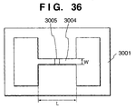
- Fig. 36 is a plan view showing the device by M. Hartwell et al. described above as a typical example of the device structures of these surface-conduction emission type electron-emitting devices.
- reference numeral 3001 denotes a substrate; and 3004, a conductive thin film made of a metal oxide formed by sputtering.
- This conductive thin film 3004 has an H-shaped pattern, as shown in Fig. 36.
- An electron-emitting portion 3005 is formed by performing electrification processing (referred to as forming processing to be described later) with respect to the conductive thin film 3004.
- An interval L in Fig. 36 is set to 0.5 to 1 mm, and a width W is set to 0.1 mm.
- the electron-emitting portion 3005 is shown in a rectangular shape at the center of the conductive thin film 3004 for the sake of illustrative convenience. However, this does not exactly show the actual position and shape of the electron-emitting portion.
- the electron-emitting portion 3005 is formed by performing electrification processing called forming processing for the conductive thin film 3004 before electron emission.
- forming processing for example, a constant DC voltage or a DC voltage which increases at a very low rate of, e.g., 1 V/min is applied across the two ends of the conductive thin film 3004 to partially destroy or deform the conductive thin film 3004, thereby forming the electron-emitting portion 3005 with an electrically high resistance.
- the destroyed or deformed part of the conductive thin film 3004 has a fissure.
- electrons are emitted near the fissure.
- the above surface-conduction emission type electron-emitting devices are advantageous because they have a simple structure and can be easily manufactured. For this reason, many devices can be formed on a wide area. As disclosed in Japanese Patent Laid-Open No. 64-31332 filed by the present applicant, a method of arranging and driving a lot of devices has been studied.
- an image display apparatus using the combination of an surface-conduction emission type electron-emitting device and a fluorescent substance which emits light upon reception of an electron beam has been studied.
- This type of image display apparatus using the combination of the surface-conduction emission type electron-emitting device and the fluorescent substance is expected to have more excellent characteristics than other conventional image display apparatuses.
- the above display apparatus is superior in that it does not require a backlight because it is of a self-emission type and that it has a wide view angle.
- an electron source manufacturing method is characterized by comprising the step of applying a potential to first portions of a plurality of conductive members serving as at least part of electron-emitting devices via a wiring commonly connected to the plurality of conductive members, and applying a potential to second portions of the plurality of conductive members, thereby applying a voltage to the plurality of conductive members, wherein the potential applied to the second portions of the plurality of conductive members is set to relax a difference in voltage applied to the plurality of conductive members owing to a difference between potentials at portions respectively connected to the first portions of the plurality of conductive members in the wiring commonly connected to the plurality of conductive members.
- the present inventors have examined surface-conduction emission type electron-emitting devices of various materials, various manufacturing methods, and various structures, in addition to the above-mentioned conventional surface-conduction emission type electron-emitting device. Further, the present inventors have made extensive studies on a multi electron-beam source having a large number of surface-conduction emission type electron-emitting devices, and an image display apparatus using this multi electron-beam source.
- the present inventors have examined a multi electron-beam source having an electrical wiring method shown in, e.g., Fig. 37. That is, a large number of surface-conduction emission type electron-emitting devices are two-dimensionally arranged in a matrix to obtain a multi electron-beam source, as shown in Fig. 37.
- numeral 4001 denotes a surface-conduction emission type electron-emitting device; 4002, a row-direction wiring; and 4003, a column-direction wiring.
- the row- and column-direction wirings 4002 and 4003 actually have finite electrical resistances, which are represented as wiring resistances 4004 and 4005 in Fig. 37.
- This wiring method is called a simple matrix wiring method.
- the multi electron-beam source is illustrated in a 6 x 6 matrix, but the size of the matrix is not limited to this.
- a number of devices enough to perform a desired image display are arranged and wired.
- a selection potential Vs is applied to the column-direction wiring 4002 on the row to be selected, and at the same time, a non-selection potential Vns is applied to the row-direction wirings 4002 on unselected rows.
- a driving potential Ve for outputting an electron beam is applied to the column-direction wirings 4003.
- a voltage (Ve - Vs) is applied to the surface-conduction emission type electron-emitting device on the selected row
- a voltage (Ve - Vns) is applied to the surface-conduction emission type electron-emitting devices on the unselected rows.
- the potentials Ve, Vs, and Vns are set to appropriate levels, an electron beam having a desired intensity must be output from only the surface-conduction emission type electron-emitting device on the selected row.
- different driving potentials Ve are applied to the respective column-direction wirings, electron beams having different intensities must be output from respective devices on the selected row. Since the surface-conduction emission type electron-emitting device has a high response speed, a time for outputting an electron beam can be changed by changing a time for applying the driving potential Ve.
- a multi electron-beam source obtained by arranging surface-conduction emission type electron-emitting devices in a simple matrix has a variety of applications. For example, when a voltage signal corresponding to image information is appropriately applied, the multi electron-beam source can be applied as an electron source for an image display apparatus.
- the present inventors have made extensive studies for improving the characteristics of the surface-conduction emission type electron-emitting device to find that activation processing is effectively performed during the manufacture.
- the electron-emitting portion of the surface-conduction emission type electron-emitting device is formed by processing (forming processing) of flowing a current through a conductive thin film to partially destroy or deform this thin film, thereby forming a fissure. If activation processing is performed subsequently, electron-emitting characteristics can be greatly improved.
- the electron-emitting portion formed by the forming processing is electrified under appropriate conditions to deposit a deposit such as carbon or carbon compound around the electron-emitting portion.
- a deposit such as carbon or carbon compound around the electron-emitting portion.
- graphite monocrystalline, graphite polycrystalline, amorphous carbon, or mixture thereof is deposited to a thickness of 500 angstroms or less around the electron-emitting portion by periodically applying a voltage pulse in a vacuum atmosphere in which an organic substance exists at an appropriate partial pressure and the total pressure is 10 -4 to 10 -5 Torr.
- These conditions are merely an example and properly changed in accordance with the material and shape of the surface-conduction emission type electron-emitting device.
- This processing can increase the emission current at the same application voltage typically 100 times or greater the emission current immediately after forming processing. (Note that the partial pressure of the organic substance in the vacuum atmosphere is desirably reduced after activation processing.)
- activation processing is desirably performed for each device in manufacturing a multi electron-beam source formed by arranging a large number of surface-conduction emission type electron-emitting devices in a simple matrix.
- the present applicant adopted a method of dividing surface-conduction emission type electron-emitting devices arranged in a matrix into a plurality of groups and sequentially applying an activation voltage in units of groups. That is, an activation voltage was sequentially applied to M x N surface-conduction emission type electron-emitting devices as shown in Fig. 38 in units of rows.
- reference symbols EY1 to EYn and EX1 to EXn denote wirings.
- Fig. 39 shows the case in which an activation voltage is applied to surface-conduction emission type electron-emitting devices (black devices in Fig. 39) on the second row.
- the wiring EX2 is connected to an activation potential source, and the remaining electrodes are set to the ground level, i.e., 0 V.
- the surface-conduction emission type electron-emitting devices on the second row receive the activation voltage in principle, and the remaining surface-conduction emission type electron-emitting devices do not receive any voltage or current.
- Activation was actually performed by this method to find that the surface-conduction emission type electron-emitting devices exhibited more uniform electron-emitting characteristics.
- an activation voltage can be applied to only surface-conduction emission type electron-emitting devices on one row in principle.
- the electrical resistances of the wirings EY1 to EYn and EX1 to EXn are not 0 in practice, a current flows to cause a potential drop.
- a model including their wiring resistances is shown in Fig. 40A.
- reference symbols F1 to FN denote surface-conduction emission type electron-emitting devices; r1 to rN, wiring resistances between devices on the row wiring EX2; and ry, a wiring resistance from the feeding terminal of each of the wirings EY1 to EYN to a corresponding surface-conduction emission type electron-emitting device.
- the row wiring EX2 is generally designed to be formed from a material having a constant line width and thickness, r1 to rN can be considered to be equal except for variations in the manufacture. Since the wirings EY1 to EYN are generally designed to be uniform, the resistances ry of the respective wirings can be considered to be equal.
- FIG. 40B A current flowing through the model shown in Fig. 40A will be explained with reference to Fig. 40B.
- I a current supplied from the activation potential source
- i1 to iN currents flowing through the surface-conduction emission type electron-emitting devices F1 to FN
- ir1 to irN be currents flowing through the wiring resistances r1 to rN of respective devices in the row direction
- the current ir1 flowing through r1 is equal to the sum of currents flowing through all surface-conduction emission type electron-emitting devices
- the current ir2 flowing through r2 is equal to the difference obtained by subtracting the current i1 flowing through the surface-conduction emission type electron-emitting device F1 from the sum of currents flowing through all surface-conduction emission type electron-emitting devices.
- the current irN flowing through rN is equal to the current iN flowing through the surface-conduction emission type electron-emitting device FN. Therefore, a row-direction wiring nearer the power source flows a larger current.
- Fig. 41 is a graph showing activation characteristics when one of surface-conduction emission type electron-emitting devices arranged in a matrix is activated. As shown in Fig. 41, when activation processing starts, the device current (If in Fig. 41) and emission current (Ie in Fig. 41) flowing through the surface-conduction emission type electron-emitting device increase along with electrification and saturate at last. That is, the current flowing through the surface-conduction emission type electron-emitting device increases along with the progress of activation processing, and the largest current flows through the surface-conduction emission type electron-emitting device at the end of activation processing.
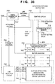
- Fig. 43A is a circuit diagram showing an electrification circuit when electrodes are extracted from two sides
- Fig. 43B shows a device application voltage distribution in this case.
- an electron source manufacturing method is characterized by comprising the step of applying a potential to first portions of a plurality of conductive members serving as at least part of electron-emitting devices via a wiring commonly connected to the plurality of conductive members, and applying a potential to second portions of the plurality of conductive members, thereby applying a voltage to the plurality of conductive members, wherein the potential applied to the second portions of the plurality of conductive members is set to relax the difference in voltage applied to the plurality of conductive members owing to the difference between potentials at portions respectively connected to the first portions of the plurality of conductive members in the wiring commonly connected to the plurality of conductive members.
- a voltage corresponding to the potential difference between the potentials of the first and second portions of the conductive member is applied to the conductive member.
- the potentials differ between respective portions on the wiring
- the potentials of the second portions of the conductive members are set equal, voltages applied between the first and second portions of the conductive members become different from each other.
- voltages applied to the first and second portions of the conductive members can be made close to each other by setting the potential of the second portion to relax the difference between voltages.
- first and second portions To substantially apply a voltage between the first and second portions, different potentials are applied to the first and second portions. Either one potential may be the ground potential.
- the conductive member which receives the voltage and serves as at least part of the electron-emitting device one having undergone, e.g., the forming step of the surface-conduction emission type electron-emitting device can be suitably used.
- a conductive film can be used as the conductive member.
- a form of a conductive member which receives the voltage a form having a high-resistance portion between the first and second portions, e.g., a gap formed between the first and second portions can be adopted.
- the voltage application step can be particularly applied to the step of depositing a deposit in or near the gap. This voltage application step is suitable when a current flowing through the conductive member increases or a current flowing through the conductive member increases or a current flowing through a wiring connected to the conductive member increases, as will be described in the following embodiments.
- the voltage application step is performed for a plurality of conductive members having first portions connected to one row wiring by a potential applied to the row wiring and a potential applied to column wirings each connected to the second portion of each conductive member.
- the potential applied to the second portion may be changed in accordance with a change in potential applied to the first portion.
- the degree of potential drop on the wiring also changes, the potential of the first portion changes, and thus the potential applied to the second portion is desirably controlled in accordance with the change in potential of the first portion.
- the potential applied to the first portion need not necessarily be measured.
- this potential can be estimated by measuring a current flowing through the conductive member.
- a circuit for automatically setting the second potential in accordance with the measured current may be employed.
- one or both of the potential applied to the first portion and the potential applied to the second portion are preferably applied as pulses.
- a potential applied to the wiring commonly connected to the plurality of conductive members and the potential applied to the second portion are applied as pulses, and the pulse-like potential applied to the wiring commonly connected to the plurality of conductive members is applied after the pulse-like potential applied to the second portion.
- the conductive member is preferably connected to one of a plurality of row wirings and one of a plurality of column wirings that constitute a matrix
- the voltage application step preferably comprises the step of applying a voltage to conductive members connected to a row wiring selected from the plurality of row wirings by a potential applied to the first portions in accordance with a potential applied to the selected row wiring and a potential applied to the second portions in accordance with a potential applied to the plurality of column wirings.
- an unselected row wiring out of the plurality of row wirings preferably receives a potential for suppressing a current flowing through the unselected row wiring owing to the potential difference from the potential applied to the column wiring.
- one or both of the potential applied to the unselected row wiring and the potential applied to the column wiring are preferably set to set the potential of the unselected row wiring to a potential between the maximum and minimum values of the potential applied to the plurality of column wirings, e.g., to an intermediate value between the maximum and minimum values.
- One or both of the potential applied to the unselected row wiring and the potential applied to the column wiring are preferably set to set the ground potential between the maximum and minimum values of the potential applied to the plurality of column wirings.
- the electron source manufacturing method preferably comprises the step of applying the voltage while sequentially switching row wirings to be selected, and more preferably comprises the step of selecting a given row wiring and applying the voltage to conductive members connected to the selected row wiring at a time interval, thereby applying the voltage and the step of selecting another row wiring during the time interval and applying the voltage to conductive members connected to this another row wiring.
- a method of manufacturing an image forming apparatus having an electron source and an image forming member for forming an image upon irradiation of electrons emitted by the electron source is characterized by comprising the steps of manufacturing the electron source by the electron source manufacturing method described above, and assembling the electron source and the image forming member.
- an electron source manufacturing apparatus is characterized by comprising a first circuit for applying a potential to first portions of a plurality of conductive members serving as at least part of electron-emitting devices via a wiring commonly connected to the plurality of conductive members, and a second circuit for applying a potential to second portions of the plurality of conductive members, wherein the second circuit sets the potential applied to the second-portions of the plurality of conductive members so as to relax a difference in voltage applied to the plurality of conductive members owing to a difference between potentials at portions respectively connected to the first portions of the plurality of conductive members in the wiring commonly connected to the plurality of conductive members.
- the apparatus preferably comprises a current monitoring circuit for monitoring a current flowing through the conductive member.
- the second circuit preferably sets the potential on the basis of a current flowing through the conductive member.
- the second circuit preferably controls the potential applied to the second portion in accordance with the application time of the potential to the second portion.
- the second circuit may comprise memory means which is referred to in order to set the potential applied to the second portion.
- the second circuit may include a circuit which generates potential differences which are equal to potential differences at the portions respectively connected to the first portions of the plurality of conductive members commonly connected in the wiring
- the configuration can be realized by, for example, sinking an electric current from each of the plurality of conductive member or supplying an electric current to each of the plurality of conductive member at predetermined points of an equivalent wiring resistance array having a resistance substantially equal to the resistance of the wiring.
- the value of the current flowing the plurality of conductive members can be acquired by monitoring the current flowing the wiring and dividing the monitored values by the number of conductive members connected with the wiring.
- the current value flowing the plurality of conductive members can be acquired by measuring a current flowing the each wiring connected with the second portion. Further, the current can be acquired according to data previously measured.
- the potentials to be applied to the respective second portions are obtained by superposing the potential distribution and an offset potential.
- the degree of potential drop can be suppressed.
- a voltage applying circuit applying a voltage to a plurality of conductive members connected with a plurality of row wirings and a plurality of column wirings which form a matrix comprising:
- the second circuit preferably has a circuit for superposing the potential distribution generated by said potential distribution generating circuit and an offset potential.
- a buffer amplifier may serve as such circuit.
- the aforementioned conductive member may have various configurations.
- the conductive member may have a pair of electrodes which pass an electric current when different potentials are applied.
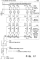
- FIG. 1 An activation apparatus for a surface-conduction emission type electron-emitting device according to an embodiment of the present invention will be described with reference to Fig. 1. First, the arrangement and manufacturing method of a display panel to which the present invention is applied will be exemplified.
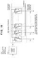
- Fig. 22 is a partially cutaway perspective view of a display panel 101 used in the embodiment in Fig. 1, showing the internal structure of the panel.
- reference numeral 1005 denotes a rear plate; 1006, a side wall; and 1007, a face plate.
- These parts 1005 to 1007 constitute an airtight container for maintaining the inside of the display panel vacuum.
- frit glass is applied to junction portions, and sintered at 400 to 500°C in air or nitrogen atmosphere, thus the parts are seal-connected. A method for exhausting air from the inside of the container will be described later.
- the N x M cold cathode devices are arranged in a simple matrix with M row-direction wirings 1003 and N column-direction wirings 1004.
- the portion constituted by the components denoted by references 1001 to 1004 will be referred to as a multi electron-beam source. The manufacturing method and structure of the multi electron-beam source will be described in detail later.
- the substrate 1001 of the multi electron-beam source is fixed to the rear plate 1005 of the airtight container. If, however, the substrate 1001 of the multi electron-beam source has sufficient strength, the substrate 1001 of the multi electron-beam source may also serve as the rear plate of the airtight container.
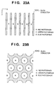
- a fluorescent film 1008 is formed on the lower surface of the face plate 1007.
- the fluorescent film 1008 is coated with red, green, and blue fluorescent substances, i.e., three primary color fluorescent substances used in the CRT field.
- the respective color fluorescent substances are formed into a striped structure, and black conductive members 1010 are provided between the stripes of the fluorescent substances.
- the purpose of providing the black conductive members 1010 is to prevent display color misregistration even if the electron-beam irradiation position is shifted to some extent, to prevent degradation of display contrast by shutting off reflection of external light, to prevent the charge-up of the fluorescent film by the electron beam, and the like.
- As a material for the black conductive members 1010 graphite is used as a main component, but other materials may be used so long as the above purpose is attained.
- three-primary colors of the fluorescent film is not limited to the stripes as shown in Fig. 23A.
- delta arrangement as shown in Fig. 23B or any other arrangement may be employed.
- a single-color fluorescent substance may be applied to the fluorescent film 1008, and the black conductive member may be omitted.
- a metal back 1009 which is well-known in the CRT field, is provided on the fluorescent film 1008 on the rear plate side.
- the purpose of providing the metal back 1009 is to improve the light-utilization ratio by mirror-reflecting part of the light emitted by the fluorescent film 1008, to protect the fluorescent film 1008 from collision with negative ions, to be used as an electrode for applying an electron-beam accelerating voltage, to be used as a conductive path for electrons which excited the fluorescent film 1008, and the like.
- the metal back 1009 is formed by forming the fluorescent film 1008 on the face plate substrate 1007, smoothing the front surface of the fluorescent film, and depositing Al thereon by vacuum deposition. Note that when fluorescent substances for a low voltage is used for the fluorescent film 1008, the metal back 1009 is not used.
- transparent electrodes made of, e.g., ITO may be provided between the face plate substrate 1007 and the fluorescent film 1008, although such electrodes are not used in this embodiment.
- Dx1 to Dxm, Dy1 to Dyn, and Hv are electric connection terminals for an airtight structure provided to electrically connect the display panel to an electric circuit (not shown).
- Dx1 to Dxm are electrically connected to the row-direction wirings 1003 of the multi electron-beam source; Dy1 to Dyn, to the column-direction wirings 1004 of the multi electron-beam source; and Hv, to the metal back 1009 of the face plate.
- an exhaust pipe and a vacuum pump are connected, and the airtight container is evacuated to a vacuum of about 10 -7 Torr. Thereafter, the exhaust pipe is sealed.
- a getter film (not shown) is formed at a predetermined position in the airtight container immediately before/after the sealing.
- the getter film is a film formed by heating and evaporating a getter material mainly consisting of, e.g., Ba, by heating or RF heating. The suction effect of the getter film maintains a vacuum of 1 x 10 -5 or 1 x 10 -7 Torr in the container.
- any material, shape, and manufacturing method for cold cathode device devices may be employed as long as an electron source can be obtained by arranging cold cathode devices in a simple matrix. Therefore, cold cathode devices such as surface-conduction emission type electron-emitting devices, FE type devices, or MIM type devices can be used.
- a surface-conduction emission type electron-emitting device of these cold cathode devices, is especially preferable. More specifically, the electron-emitting characteristic of an FE type device is greatly influenced by the relative positions and shapes of the emitter cone and the gate electrode, and hence a high-precision manufacturing technique is required to manufacture this device. This poses a disadvantageous factor in attaining a large display area and a low manufacturing cost. According to an MIM type device, the thicknesses of the insulating layer and the upper electrode must be decreased and made uniform. This also poses a disadvantageous factor in attaining a large display area and a low manufacturing cost.
- a surface-conduction emission type electron-emitting device can be manufactured by a relatively simple manufacturing method, and hence an increase in display area and a decrease in manufacturing cost can be attained.
- the present inventors have also found that among the surface-conduction emission type electron-emitting devices, an electron beam source having an electron-emitting portion or its peripheral portion consisting of a fine particle film is excellent in electron-emitting characteristic and can be easily manufactured. Such a device can therefore be most suitably used for the multi electron-beam source of a high-brightness, large-screen image display apparatus.
- surface-conduction emission type electron-emitting devices each having an electron-emitting portion or its peripheral portion made of a fine particle film are used.
- the basic structure, manufacturing method, and characteristics of the preferred surface-conduction emission type electron-emitting device will be described first.
- the structure of the multi electron-beam source having many devices arranged in a simple matrix will be described later.
- Typical examples of surface-conduction emission type electron-emitting devices each having an electron-emitting portion or its peripheral portion made of a fine particle film include two types of devices, namely flat and step type devices.
- FIGs. 24A and 24B are a plan view and a sectional view, respectively, for explaining the structure of the flat surface-conduction emission type electron-emitting device.
- reference numeral 1101 denotes a substrate; 1102 and 1103, device electrodes; 1104, a conductive thin film; 1105, an electron-emitting portion formed by the forming processing; and 1113, a thin film formed by the activation processing.
- various glass substrates of, e.g., quartz glass and soda-lime glass, various ceramic substrates of, e.g., alumina, or any of those substrates with an insulating layer formed thereon can be employed.
- conductive material for example, any material of metals such as Ni, Cr, Au, Mo, W, Pt, Ti, Cu, Pd and Ag, or alloys of these metals, otherwise metal oxides such as In 2 O 3 -SnO 2 , or semiconductive material such as polysilicon, can be employed.
- These electrodes 1102 and 1103 can be easily formed by the combination of a film-forming technique such as vacuum-evaporation and a patterning technique such as photolithography or etching, however, any other method (e.g., printing technique) may be employed.
- the shape of the electrodes 1102 and 1103 is appropriately designed in accordance with an application object of the electron-emitting device.
- an interval L between electrodes is designed by selecting an appropriate value in a range from hundreds angstroms to hundreds micrometers. Most preferable range for a display apparatus is from several micrometers to ten micrometers.
- electrode thickness d an appropriate value is selected in a range from hundreds angstroms to several micrometers.
- the conductive thin film 1104 comprises a fine particle film.
- the "fine particle film” is a film which contains a lot of fine particles (including masses of particles) as film-constituting members. In microscopic view, normally individual particles exist in the film at predetermined intervals, or in adjacent to each other, or overlapped with each other.
- One particle has a diameter within a range from several angstroms to thousand angstroms. Preferably, the diameter is within a range from 10 angstroms to 200 angstroms.
- the thickness of the fine particle film is appropriately set in consideration of conditions as follows. That is, condition necessary for electrical connection to the device electrode 1102 or 1103, condition for the forming processing to be described later, condition for setting electrical resistance of the fine particle film itself to an appropriate value to be described later etc.
- the thickness of the film is set in a range from several angstroms to thousand angstroms, more preferably, 10 angstroms to 500 angstroms.
- Materials used for forming the fine particle film are, e.g., metals such as Pd, Pt, Ru, Ag, Au, Ti, In, Cu, Cr, Fe, Zn, Sn, Ta, W and Pb, oxides such as PdO, SnO 2 , In 2 O 3 , PbO and Sb 2 O 3 , borides such as HfB 2 , ZrB 2 , LaB 6 , CeB 6 , YB 4 and GdB 4 , carbides such as TiC, ZrC, HfC, TaC, SiC, and WC, nitrides such as TiN, ZrN and HfN, semiconductors such as Si and Ge, and carbons. Any of appropriate material(s) is appropriately selected.
- metals such as Pd, Pt, Ru, Ag, Au, Ti, In, Cu, Cr, Fe, Zn, Sn, Ta, W and Pb
- oxides such as PdO, SnO 2 , In 2 O 3 , P
- the conductive thin film 1104 is formed with a fine particle film, and sheet resistance of the film is set to reside within a range from 10 3 to 10 7 ( ⁇ /sq).
- the conductive thin film 1104 is electrically connected to the device electrodes 1102 and 1103, they are arranged so as to overlap with each other at one portion.
- the respective parts are overlapped in order of, the substrate, the device electrodes, and the conductive thin film, from the bottom. This overlapping order may be, the substrate, the conductive thin film, and the device electrodes, from the bottom.
- the electron-emitting portion 1105 is a fissured portion formed at a part of the conductive thin film 1104.
- the electron-emitting portion 1105 has a resistance characteristic higher than peripheral conductive thin film.
- the fissure is formed by the forming processing to be described later on the conductive thin film 1104. In some cases, particles, having a diameter of several angstroms to hundreds angstroms, are arranged within the fissured portion. As it is difficult to exactly illustrate actual position and shape of the electron-emitting portion, therefore, Figs. 24A and 24B show the fissured portion schematically.
- the thin film 1113 which comprises carbon or carbon compound material, covers the electron-emitting portion 1115 and its peripheral portion.
- the thin film 1113 is formed by the activation processing to be described later after the forming processing.
- the thin film 1113 is preferably graphite monocrystalline, graphite polycrystalline, amorphous carbon, or mixture thereof, and its thickness is 500 angstroms or less, more preferably, 300 angstroms or less.
- Figs. 24A and 24B show the film schematically.
- Fig. 24A shows the device where a part of the thin film 1113 is removed.
- the preferred basic structure of the surface-conduction emission type electron-emitting device is as described above.
- the device has the following constituents.
- the substrate 1101 comprises a soda-lime glass, and the device electrodes 1102 and 1103, an Ni thin film.
- the electrode thickness d is 1,000 angstroms and the electrode interval L is 2 ⁇ m.
- the main material of the fine particle film is Pd or PdO.
- the thickness of the fine particle film is about 100 angstroms, and its width W is 100 ⁇ m.
- Figs. 25A to 25D are sectional views showing the manufacturing processes of the surface-conduction emission type electron-emitting device. Note that reference numerals are the same as those in Fig. 24B.
- reference numeral 1114 denotes an anode electrode, connected to a direct-current (DC) high-voltage power source 1115 and a galvanometer 1116, for capturing emission current Ie emitted from the surface-conduction emission type electron-emitting device.
- DC direct-current
- galvanometer 1116 for capturing emission current Ie emitted from the surface-conduction emission type electron-emitting device.
- the galvanometer 1116 While applying voltage from the activation power source 1112, the galvanometer 1116 measures the emission current Ie, thus monitors the progress of activation processing, to control the operation of the activation power source 1112.
- Fig. 27B shows an example of the emission current Ie measured by the galvanometer 1116.
- the emission current Ie increases with elapse of time, gradually comes into saturation, and almost never increases then.
- the voltage application from the activation power source 1112 is stopped, then the activation processing is terminated.
- the above electrification conditions are preferable to the surface-conduction emission type electron-emitting device of the embodiment.
- the conditions are preferably changed in accordance with the change of device design.
- the surface-conduction emission type electron-emitting device as shown in Fig. 25E is manufactured.
- Fig. 28 is a sectional view schematically showing the basic construction of the step surface-conduction emission type electron-emitting device.
- reference numeral 1201 denotes a substrate; 1202 and 1203, device electrodes; 1206, a step-forming member for making height difference between the electrodes 1202 and 1203; 1204, a conductive thin film using a fine particle film; 1205, an electron-emitting portion formed by the forming processing; and 1213, a thin film formed by the activation processing.
- the step-forming member 1206 differs from the above-described flat device. Difference between the step device from the above-described flat device is that one of the device electrodes (1202 in this example) is provided on the step-forming member 1206 and the conductive thin film 1204 covers the side surface of the step-forming member 1206.
- the device interval L in Fig. 24A is set in this structure as a height difference Ls corresponding to the height of the step-forming member 1206.
- the substrate 1201, the device electrodes 1202 and 1203, the conductive thin film 1204 using the fine particle film can comprise the materials given in the explanation of the flat surface-conduction emission type electron-emitting device.
- the step-forming member 1206 comprises electrically insulating material such as SiO 2 .
- Figs. 29A to 29F are sectional views showing the manufacturing processes.
- reference numerals of the respective parts are the same as those in Fig. 28.
- the stepped surface-conduction emission type electron-emitting device shown in Fig. 29F is manufactured.
- the structure and manufacturing method of the flat surface-conduction emission type electron-emitting device and those of the stepped surface-conduction emission type electron-emitting device are as described above. Next, the characteristic of the electron-emitting device used in the display apparatus will be described below.
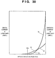
- Fig. 30 shows a typical example of (emission current Ie) to (device voltage (i.e., voltage to be applied to the device) Vf) characteristic and (device current If) to (device application voltage Vf) characteristic of the device used in the display apparatus. Note that compared with the device current If, the emission current Ie is very small, therefore it is difficult to illustrate the emission current Ie by the same measure of that for the device current If. In addition, these characteristics change due to change of designing parameters such as the size or shape of the device. For these reasons, two lines in the graph of Fig. 30 are respectively given in arbitrary units.
- the device used in the display apparatus has three characteristics as follows:
- threshold voltage Vth voltage of a predetermined level
- the emission current Ie drastically increases, however, with voltage lower than the threshold voltage Vth, almost no emission current Ie is detected.
- the device has a nonlinear characteristic based on the clear threshold voltage Vth.
- the emission current Ie changes in dependence upon the device application voltage Vf. Accordingly, the emission current Ie can be controlled by changing the device voltage Vf.
- the emission current Ie is output quickly in response to application of the device voltage Vf to the device. Accordingly, an electrical charge amount of electrons to be emitted from the device can be controlled by changing period of application of the device voltage Vf.
- the surface-conduction emission type electron-emitting device with the above three characteristics is preferably applied to the display apparatus.
- the first characteristic is utilized, display by sequential scanning of display screen is possible.
- the threshold voltage Vth or greater is appropriately applied to a driven device in accordance with a desired emission luminance, while voltage lower than the threshold voltage Vth is applied to an unselected device. In this manner, sequentially changing the driven devices enables display by sequential scanning of display screen.
- emission luminance can be controlled by utilizing the second or third characteristic, which enables multi-gradation display.
- Fig. 31 is a plan view of the multi electron-beam source used in the display panel in Fig. 22.
- Fig. 32 shows a cross-section cut out along the line A - A' in Fig. 31.
- a multi electron-beam source having such a structure is manufactured by forming the row- and column-direction wirings 1003 and 1004, the inter-electrode insulating layers (not shown), and the device electrodes and conductive thin films of the surface-conduction emission type electron-emitting devices on the substrate, then supplying electricity to the respective devices via the row- and column-direction wirings 1003 and 1004, thus performing the forming processing and the activation processing.
- a plurality of surface-conduction emission type electron-emitting devices are arranged in a matrix on a surface-conduction emission type electron-emitting device substrate 101 to be activated, and have already undergone forming processing.
- the substrate 101 is connected to an evacuation device (not shown) and evacuated to about 10 -4 to 10 -5 Torr.
- the substrate 101 is further connected to an external electric circuit via row-direction wiring terminals Dx1 to Dxm and column-direction wiring terminals Dy1 to Dyn.
- a line selection circuit 102 for selecting a line to be activated selects a row-direction wiring in accordance with an instruction from a timing generation circuit 105, and applies a selection potential of a power source 104 to the selected row-direction wiring.
- a current monitoring circuit 103 monitors a current flowing through the selected row upon applying the selection potential to the selected row-direction wiring.
- the current monitoring circuit 103 is made up of a detection resistance Rmon and a measurement amplifier for measuring a potential difference generated across the resistance. With these components, the current monitoring circuit 103 detects the current If and outputs it as an activation current value 109 to a control circuit 106. Note that the resistance value of the detection resistance Rmon is set small enough to prevent influence on an application voltage to the surface-conduction emission type electron-emitting device by a potential drop caused by the flowing device current If.
- the power source 104 generates a potential to be applied to the row-direction wiring of the electron source in accordance with a command value from the control circuit 106.
- a buffer amplifier circuit 107 drives the column-direction wiring terminals Dy1 to Dyn of the surface-conduction emission type electron-emitting device substrate 101 at a timing synchronized with a control clock signal Hscan from the timing generation circuit 105.
- An input value to the buffer amplifier i.e., a potential amplitude value for driving the terminals Dy1 to Dyn is determined by a potential distribution generation circuit 108.
- the progress of activation is grasped by detecting a current amount flowing upon activation, i.e., the activation current 109 as output data from the current monitoring circuit 103.
- the control circuit 106 starts activation in response to an activation start command, and sequentially corrects the potential distribution of devices in the column direction that changes with the progress of activation, as will be described in detail later. That is, the control circuit 106 estimates a device current flowing through each device using an output from the current monitoring circuit 103, and sets the estimated value as a current setting value 110 in the potential distribution generation circuit 108.
- the potential distribution generation circuit 108 calculates a potential distribution generated in devices in the column direction in accordance with the current setting value 110 and generates this distribution as a potential.
- the calculated potential is applied to the column-direction electrode of each device via the buffer amplifier 107.
- a potential distribution generated by the device current and wiring resistance is corrected to suppress the difference in voltage applied to the device.
- the potential distribution is corrected until the end of activation by sequentially updating data of the potential distribution generation circuit 108 in accordance with the progress of activation.
- the line selection circuit 102 will be described with reference to Fig. 2.
- This circuit incorporates m switching elements (SWX1 to SWXm). Each switching element selects either one of the output potential of the power source 104 and 0 V (ground level), and the m switching elements are electrically connected to the terminals Dx1 to Dxm of the surface-conduction emission type electron-emitting device substrate 101, respectively. Each switching element operates based on a control signal Vscan output from the timing generation circuit 105. In practice, the switching elements can be easily constituted by a combination of switching elements such as FETs or relays. In Fig. 2, the first line (Sx1) is selected, the output potential of the power source 104 is applied to only the row-direction wiring Dx1, and the remaining lines are grounded.
- Fig. 3 is a circuit diagram showing the arrangement of the potential distribution generation circuit 108.
- the circuit 108 operates to automatically calculate a compensation potential amount to be applied in the column direction and output it to the buffer amplifier 107 in order to compensate a potential drop caused by a device current flowing through each device and a row-direction wiring resistance (r1 to rN in Fig. 40) along with the progress of activation, as described above.
- the potential distribution generation circuit 108 is made up of an equivalent wiring resistance array 301 and a constant current circuit 302.
- the equivalent wiring resistance array 301 is a resistance array having a value equivalent to the wiring resistance on a given row wiring of the surface-conduction emission type electron-emitting device substrate 101 having a simple matrix arrangement (see Fig. 40). Resistances rd1 to rdN are set equal to the values r1 to rN of the wiring resistances of respective portions on the row wiring. Although a method of forming an electrode on the surface-conduction emission type electron-emitting device substrate 101 will be described below, the electrode is designed to be formed from a material having a constant line width and thickness, rd1 to rdN can be considered to be equal except for variations in the manufacture.
- the equivalent wiring resistance array 301 can therefore be constituted by aligning simulation resistances equal to an actual resistance value on an array.
- an extra wiring for one line may be formed at the end of the surface-conduction emission type electron-emitting device substrate 101 and extracted to constitute the equivalent wiring resistance array 301.
- the constant current circuit 302 includes a total of n constant current circuits each made up of a transistor and resistance R in correspondence with the column-direction wiring terminals Dy1 to Dyn of the surface-conduction emission type electron-emitting device substrate 101. Each constant current circuit operates to sink a current amount: (Base Input Potential - 0.6 + V)/R Note that the transistors of the constant current circuit 302 share a base, which receives a current setting value 303 as an input potential. Accordingly, all the constant current circuits operate to have the same current setting value.
- Activation is performed to set the device currents of all devices to a target value. This target current value is determined in advance from a necessary electron-emitting amount or the like.
- activation processing is performed while monitoring an output from the current monitoring circuit 103 so as to set the device currents of respective devices on the surface-conduction emission type electron-emitting device substrate 101 to 2 mA at last.
- control circuit 106 when the control circuit 106 receives an activation start command, it controls the timing generation circuit 105 and power source 104 in order to perform electrification processing in units of rows.
- the control circuit 106 sets the current setting value 110 so as to set the column-direction wiring terminals Dy1 to Dyn to the ground potential, and sequentially applies pulses of the activation potential Eac to the row-direction wiring terminals Dx1 to Dxm.
- This pulse has, for example, a pulse width of 1 msec and a pulse height of 18 V. Then, the pulse potentials are sequentially applied to the surface-conduction emission type electron-emitting device substrate 101 in units of rows to start activation in units of lines.
- the first embodiment will exemplify activation when n devices on the line of the row-direction wiring terminal Dx1 are activated.
- a surface-conduction emission type electron-emitting device group 401 is represented by a model including the wiring resistance, and the state in which this device group is activated will be explained with reference to Fig. 4.
- reference symbols F1 to Fn denote surface-conduction emission type electron-emitting devices on the line of the row-direction wiring terminal Dx1; r1 to rn, wring resistances at respective portions on a row wiring Ex1; and Ry, a wiring resistance from the feeding terminal of each of the wirings Dy1 to Dyn to a corresponding surface-conduction emission type electron-emitting device.
- the row wiring is designed to be formed from a material having a constant line width and thickness in the first embodiment, r1 to rN can be considered to be equal except for variations in the manufacture. Since the wirings are designed to be uniform, the resistances Ry of the respective wirings can be considered to be equal. Although the equivalent resistance value of the surface-conduction emission type electron-emitting device changes (decreases) before and after activation, the equivalent resistance of each device is much higher than the value Ry, and Ry is substantially negligible in the first embodiment. The equivalent resistance value of the surface-conduction emission type electron-emitting device is designed higher than r1 to rN.
- the control circuit 106 controls the line selection circuit 102 via the timing generation circuit 105, and connects the power source 104 for outputting the activation potential Eac and the current monitoring circuit 103 to the row-direction wiring terminal Dx1.
- the terminal Dx1 receives the activation potential Eac.
- the terminals Dy1 to Dyn as other electrode terminals of devices on the line Dx1 are driven by the buffer amplifier 107.
- the buffer amplifier 107 operates to sink activation currents i1 to in from the devices F1 to FN, and the output potential amplitude is determined by the potential distribution generation circuit 108.
- the potential distribution circuit 108 is made up of the equivalent wiring resistance array 301 and constant current circuit 302, as described above.
- the resistance values rd1 to rdn of the equivalent wiring resistance array 301 are set equal to the wiring resistance values r1 to rn of the row wiring Dx1.
- N constant current sources CI1 to CIn constituting the constant current circuit 302 correspond to the devices F1 to FN of the surface-conduction emission type electron-emitting device group 401, and equivalently replace device currents flowing through the devices along with the progress of activation.
- the electrical characteristics of the device change as shown in Fig. 41. That is, the device current does not substantially flow at the start of activation, starts flowing at the same time as electrification, and saturates.
- the terminal potential of the device group on the row wiring Dx1 is monitored to find changes in potentials Gy1 to Gyn due to the influence of the wiring resistances r1 to rn. The potential change increases with the progress of activation and maximizes at the end of activation.
- ⁇ V 1/2 ⁇ 1000 ⁇ 1001 ⁇ 2 mA ⁇ 10m ⁇ ⁇ 10 V occurs at the terminal Gyn of the device Fn farthest from the feeding terminal.
- Figs. 5A and 5B show the distributions of potentials applied across the devices F1 to Fn at the start and end of activation.
- Fig. 5A shows a potential distribution immediately after the start of activation.
- the abscissa represents device numbers F1 to Fn, which indicate device positions.
- the current setting value of the potential distribution generation circuit 108 is almost 0, and the outputs By1 to Byn of the potential distribution generation circuit 108 and the outputs Sy1 to Syn of the buffer 107 are also at almost 0 V. For this reason, a predetermined application voltage up to 18 V is applied to the respective devices to progress activation.
- Fig. 5B shows a potential distribution at the end of activation.
- the current setting value of the potential distribution generation circuit 108 is set to 2 mA, the outputs By1 to Byn of the potential distribution generation circuit 108 and the outputs Sy1 to Syn of the buffer 107 have the same distribution as Gy1 to Gyn.
- a predetermined application voltage up to 18 V is applied to the respective devices to activate them.
- the control circuit 106 obtains a device current value in accordance with equation (1) from a current value detected by the current monitoring circuit 103 along with the progress of activation, and sets a current value corresponding to the obtained value as the current setting value of the potential distribution generation circuit 108. In this way, the outputs By1 to Byn of the potential distribution generation circuit 108 are sequentially updated to activate all devices by a constant voltage from the start to end of activation. When the device current of each device reaches 2 mA, activation ends.
- the outputs By1 to Byn of the potential distribution generation circuit 108 described in the first embodiment have a very high response speed in updating the current setting value, so that the distribution can be updated every time a pulse voltage is applied from the power source 104.
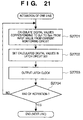
- Fig. 15 shows an example of a control procedure by the control circuit 106 when activation is performed by a procedure of completing activation in units of lines and switching lines.
- Fig. 15 shows a procedure for one line. Since the substrate 101 generally has a plurality of lines, this control procedure is repeatedly executed for a plurality of lines.
- the control circuit 106 calculates the average device current iave from an input value from the current monitoring circuit (step S3401). Since the device current is very small before activation, as shown in Fig. 5A, the first pulse can be set to iave ⁇ 0 or to an initial value obtained experimentally.
- the control circuit 106 updates the current setting value 110 in accordance with the obtained device current value (step S3402). In this state, the control circuit 106 applies the activation potential to a selected line (step S3403). Upon completion of a predetermined activation procedure for the selected line, activation for this line ends (YES in step S3404). If a next line exists, the control circuit 106 outputs a line switching signal to select the next line.
- control circuit 106 If activation for the selected line has not been completed yet, the control circuit 106 returns to step S3401 to read an activation current value with respect to the activation potential applied in step S3403 from the current monitoring circuit 103, update the current setting value, and apply a next pulse to the selected line. This is repeatedly executed until activation ends.
- the line selection circuit 102 is switched to activate another activation line.
- a plurality of lines may be simultaneously activated while sequentially switching activation lines.
- the progress of activation may vary between lines.
- the average device currents of respective lines are sequentially stored in a memory or the like, and activation is performed while updating the output of the potential distribution generation circuit 108 at a high speed using the average device current stored in the memory in switching lines. Consequently, uniform activation can be realized.
- activation is completed in units of lines. When a plurality of lines are activated parallel while sequentially switching lines, a line switching signal must be output between steps S3403 and S3404.
- a plurality of lines may be simultaneously driven.
- the current monitoring circuit 103 detects the sum of device currents for the plurality of lines. Consideration must be taken in estimating the current setting value set in the potential distribution generation circuit 108.
- the power source 104 has a positive output, and activation is performed to flow a current from the terminal Dx1 to the terminals Dy1 to Dyn.
- the polarity may be inverted, and activation may be performed to flow a current from the terminals Dy1 to Dyn to the terminal Dx1.
- the buffer amplifier 107 is constituted as a (-1)-time inverting buffer amplifier to source the current, thereby obtaining the same effects.
- the activation apparatus of the first embodiment can make the electron-emitting characteristics of all devices uniform.
- This electron source substrate is used to realize a high-quality image display apparatus almost free from variations in luminance or density.
- a surface-conduction emission type electron-emitting device substrate 601 is different from the substrate 101 in Fig. 1 in that row-direction wiring terminals Dx1 to Dxm are arranged on two sides.
- the terminals Dx1 to Dxm extracted from the two sides as shown in Fig. 6 are connected to corresponding terminals on the same lines, and connected to a line selection circuit 602.
- Fig. 43A shows an equivalent circuit when the surface-conduction emission type electron-emitting device substrate 601 according to the second embodiment is activated.
- Fig. 43B shows a device application potential distribution when devices on the second line are activated in Fig. 43A. In two-side extraction, the distribution has a mirror-symmetrical profile.
- a potential distribution amount to be applied to column-direction wiring terminals Dy1 to Dyn in Fig. 6 also has a mirror-symmetrical profile.
- This potential distribution can be reproduced by constituting a potential distribution circuit 608 by 1 to (n/2) resistance arrays and constant current sources. If the output impedance of a buffer 607 is set sufficiently low, the circuit can be simplified by preparing (n/2) buffer amplifiers 607, and commonly connecting and driving terminals (e.g.; Dy1 and Dyn, Dy2 and Dyn-1, and the like) having a symmetrical potential distribution.
- a potential distribution circuit 608 by 1 to (n/2) resistance arrays and constant current sources.
- the output Sy1 of the first column extending from the buffer amplifier is connected to the terminals Dy1 and Dyn
- the output Sy2 of the second column is connected to the terminals Dy2 and Dyn-1,...
- the output Syj of the jth column is connected to the terminals Dyj and Dyn-j+1 . If n is an odd number, the output of the (n+1)/2 column is connected to only the terminal Dy(n+1)/2 .
- Fig. 7 shows the potential distribution of respective devices upon driving in the second embodiment. As described above, a mirror-symmetrical potential distribution profile can be obtained.
- the driving potentials Sy1 to Syn of the column-direction wiring terminals Dy1 to Dyn also change with the progress of activation and are compensated to always apply a predetermined activation voltage to respective devices.
- the apparatus of the second embodiment allows manufacturing an electron source in which all devices have uniform electron-emitting characteristics.
- a surface-conduction emission type electron-emitting device substrate 801 is the same as the substrate 101 in Fig. 1.
- the operation of the whole apparatus, the activation procedure, and the like are the same as in the first embodiment, and a description thereof will be omitted.
- the third embodiment is slightly different from the first embodiment in driving method in which an output from a potential distribution circuit 808 is not directly applied to column-direction wiring terminals Dy1 to Dyn, as will be described.
- a surface-conduction emission type electron-emitting device group 901 is represented by a model including the wiring resistance, and the state in which this device group is activated will be explained with reference to Fig. 9.
- reference symbols F1 to Fn denote surface-conduction emission type electron-emitting devices on the line of a row-direction wiring terminal Dx1; r1 to rn, wring resistances at respective portions on a row wiring Ex1; and Ry, a wiring resistance from the feeding terminal of each of the wirings Dy1 to Dyn to a corresponding surface-conduction emission type electron-emitting device.
- a control circuit 806 controls a line selection circuit 802 via a timing generation circuit 805, and connects a power source 804 for outputting the activation potential Eac and a current monitoring circuit 803 to the row-direction wiring terminal Dx1.
- the terminal Dx1 is driven by the activation potential Eac.
- the terminals Dy1 to Dyn as other column-direction terminals of devices on the line Dx1 are driven by a buffer amplifier 807.
- the buffer amplifier 807 operates to sink activation currents i1 to in from the devices F1 to FN, and the output potential amplitude is determined by the potential distribution generation circuit 808. This operation is the same as in the first embodiment.
- a potential distribution produced along with the progress of activation is generated by the potential distribution generation circuit 808, and the terminals Dy1 to Dyn are driven by outputs Sy1 to Syn from the buffer amplifier 807 so as to cancel the potential distribution.
- output potential values By1 to Byn from the potential distribution circuit 808 are not directly applied to the terminals, but are added to an offset setting value 812 by the buffer amplifier 807 and then applied to the terminals,.
- This offset setting value 812 is also added to an activation potential and applied as the amplitude of the power source 804.
- the offset potential is added owing to the following reason.
- a potential drop distribution generated in the column direction on the same row is compensated by application potentials from the column-direction wiring terminals Dy1 to Dyn.
- the application potentials from the column-direction wiring terminals Dy1 to Dyn are applied to not only devices on an activated line but also devices on an inactivated line because surface-conduction emission type electron-emitting devices are arranged in a simple matrix.
- the potentials of the column-direction wiring terminals Dy1 to Dyn are as low as several V in maximum, so no problem arises even if these potentials are applied to devices on an inactivated line.
- the offset potential is added to minimize the absolute values of potentials applied from the column-direction wiring terminals Dy1 to Dyn, thereby driving the terminals Dy1 to Dyn.
- the offset potential value to be added is determined as follows.
- Figs. 10A and 10B show the potential distributions of respective devices upon driving in the third embodiment.
- Fig. 10A shows a potential difference immediately after activation.
- the offset potential value 821 is almost 0 V, and the potential distribution is almost the same as in Fig. 5A of the first embodiment.
- the offset potential 821 is generated to obtain a potential distribution profile like the one shown in Fig. 10B.
- the potential distribution of respective devices is the same as in Fig.
- Fig. 10B also shows the state in which the potential applied from the row-direction wiring terminal Dx1 also changes to 18 V + Voff along with this.
- the offset potential determination method is not limited to the above one, and the offset potential may be determined to minimize the power value applied to the entire surface-conduction emission type electron-emitting device substrate.
- a surface-conduction emission type electron-emitting device substrate 1101 is the same as the substrate 101 in Fig. 1.
- the operation of the whole apparatus, the activation procedure, and the like are the same as in the first embodiment, and a description thereof will be omitted.
- the fourth embodiment is slightly different from the first embodiment in arrangements of a current monitoring circuit 1103 and a potential distribution circuit 1108, as will be described. That is, the current monitoring circuit 1103 is interposed between column-direction wiring terminals Dy1 to Dyn and a buffer amplifier 1107 to individually monitor device currents flowing through respective devices upon activation.
- a surface-conduction emission type electron-emitting device group 1201 is represented by a model including the wiring resistance, and the state in which this device group is activated will be explained with reference to Fig. 12.
- a potential distribution produced along with the progress of activation is generated by the potential distribution generation circuit 1108, and the terminals Dy1 to Dyn are driven by outputs Sy1 to Syn from the buffer amplifier 1107 so as to cancel the potential distribution.
- the arrangement of a constant current circuit 302 constituting the potential distribution circuit 1108 is slightly different from that in the above embodiments.
- the constant current circuit 302 is changed to individually set the current setting values of n constant current sources constituting the constant current circuit 302.
- the circuit arrangement is changed from the circuit of Fig. 3 so as to individually set the base potentials of transistors constituting the constant current sources.
- current setting values 1110 corresponding to the n constant current sources can be externally supplied to individually drive the constant current sources in the potential distribution circuit 1108 shown in Fig. 12.
- the current monitoring circuit 1103 is changed to individually monitor device currents flowing through respective devices.
- the current monitoring circuit 1103 is made up of detection resistances Rmon and a measurement amplifier for measuring a voltage generated across each detection resistance Rmon. With these components, the current monitoring circuit 103 detects the currents If and outputs n detected activation current values 1109. Note that the resistance value of the detection resistance Rmon is set small enough to prevent influence on an application potential to the surface-conduction emission type electron-emitting device by a potential drop caused by the flowing device current If.
- the potential drop distribution at terminals Gy1 to Gyn along with the progress of activation can be more accurately reproduced by outputs By1 to Byn from the potential distribution circuit 1108.
- the above-described embodiments estimate current values flowing through respective devices from an activation current for one line, and control an output from the potential distribution generation circuit 108 on the assumption that activation of the devices F1 to Fn uniformly progresses and the device currents i1 to in flowing through respective devices are almost equal. In the fourth embodiment, however, a more accurate potential distribution can be reproduced by individually monitoring the activation currents of respective devices.
- the activation current values of respective devices are supplied as current setting values to constant current sources CI1 to CIn on each row in the potential distribution circuit 1108, and potentials in accordance with a potential distribution in an activated line are applied to the terminals Dy1 to Dyn via the outputs Sy1 to Syn of the buffer amplifier 1107. That is, the first embodiment employs the average value iave as a device current, whereas the fourth embodiment employs a device current measured for each device. Consequently, voltages applied between the terminals of the devices F1 to Fn can be made uniform regardless of the device position and the progress of activation.
- Ix Device Current Flowing Through Device Fx Upon Application of 18 V + Current Flowing Through Inactivated Device (m-1) Connected to Terminal Dyx Upon Application of Potential Syx
- the first term is a true device current, and the current amount of the second term is an error.
- the difference between the potential Sy and the potential of an unselected line is small, and the current amount of the second term is small to a negligible degree. To more accurately measure the current, the following steps are executed.
- a surface-conduction emission type electron-emitting device substrate 1301 is the same as the substrate 101 in Fig. 1.
- the operation of the whole apparatus, the activation procedure, and the like are the same as in the first embodiment, and a description thereof will be omitted.
- the arrangement of a current monitoring circuit 1303 is the same as in the fourth embodiment.
- the current monitoring circuit 1303 is interposed between column-direction wiring terminals Dy1 to Dyn and a buffer amplifier 1307 to individually monitor device currents flowing through respective devices upon activation.
- the fifth embodiment is slightly different from the fourth embodiment in arrangement of a potential distribution circuit 1308. That is, a control circuit 1306 calculates a potential distribution amount from activation current values flowing through devices, and transfers a digital output value corresponding to the potential distribution obtained from the calculation result to the potential distribution generation circuit.
- a surface-conduction emission type electron-emitting device group 1401 is represented by a model including the wiring resistance, and the state in which this device group is activated will be explained with reference to Fig. 14.
- the terminals Dy1 to Dyn are driven by outputs Sy1 to Syn from the buffer amplifier 1307 so as to cancel a potential distribution produced along with the progress of activation.
- the potential distribution circuit 1308 is constituted by n D/A converters 1402 and n latch circuits 1403. With this arrangement, digital output setting values 1310 corresponding to the n D/A converters are externally supplied to individually drive the D/A converters.
- the digital output setting value 1310 is set as a potential drop distribution amount calculated by the control circuit 1306. Independent potentials are set in the respective D/A converters, and all the outputs are simultaneously updated by a latch CLK 1311.
- the current monitoring circuit 1303 can individually monitor device currents flowing through respective devices.
- the current monitoring circuit 1303 is made up of detection resistances Rmon and a measurement amplifier for measuring a voltage generated across each detection resistance Rmon. With these components, the current monitoring circuit 103 detects the currents If and outputs n detected activation current values 1309.
- a device potential distribution generated along with the progress of activation is calculated as follows.
- device current values i1 to in flowing through devices F1 to Fn are obtained from the current monitoring circuit 1303, potentials By1 to Byn to be output to the output terminals of the potential distribution circuit 1308 are calculated using the wiring resistance values r1 to rn:
- Byn -rn ⁇ in + Byn - 1 + Byn - 2 +...+ By1
- the control circuit 1306 sequentially updates the output potentials By1 to Byn by the above equations, and transfers corresponding digital output data to the latch circuits 1403 of the potential distribution circuit 1308.
- the control circuit 1306 applies the latch clock 1311 to all the latch circuits 1403 in order to update D/A data, and updates the data in synchronism with this.
- the potential distribution circuit 1308 generates a potential distribution corresponding to a potential distribution amount generated at the terminals Gy1 to Gyn of the devices F1 to Fn. Note that when the number n of devices is large, a long time may be spent for a series of operations: measurement of the device current ⁇ calculation of output data data ⁇ transfer. This time can be shortened by parallel processing for respective devices.
- the output setting value is a digital value, and no constant current circuit or equivalent wiring resistance array is used. This can prevent a nonuniform activation voltage generated by the difference between the lines, such as the difference between a wiring resistance distribution on a line to be activated and a resistance value distribution in the equivalent wiring resistance array.
- a surface-conduction emission type electron-emitting device substrate 101 is the same as the substrate 101 in Fig. 1.
- the operation of the whole apparatus, the activation procedure, and the like are the same as in the first embodiment, and a description thereof will be omitted.
- the arrangement of a potential distribution circuit 1608 is the same as in the fifth embodiment, and a control circuit transfers a digital output value corresponding to a potential distribution to the potential distribution generation circuit.
- a control circuit 1606 outputs a latch clock 111 to the potential distribution generation circuit 1608.
- the remaining arrangement is the same as in the first embodiment.
- the control circuit 1606 detects the progress of activation by a current amount flowing upon activation, i.e., an activation current 109 as output data from a current monitoring circuit 103.
- the control circuit 1606 starts activation in response to an activation start command, and sequentially corrects the potential distribution of devices in the column direction that changes with the progress of activation, as will be described in detail later. That is, the control circuit 1606 estimates a device current flowing through each device using an output from the current monitoring circuit 103, and calculates a potential distribution generated in devices in the column direction from the estimated value.
- a voltage distribution generated in respective devices by the activation current and row-direction wiring resistance is corrected to apply a constant voltage across all devices on an activated lines.
- sequentially updating data of the potential distribution circuit 1608 in accordance with the progress of activation the potential distribution is corrected until the end of activation.
- Fig. 17 is a circuit diagram showing the arrangement of the potential distribution generation circuit 1608 to explain the state in which a given line is activated using the potential distribution circuit 1608.
- the potential distribution generation circuit 1608 generates a compensation potential amount to be applied in the column direction and outputs it to the buffer amplifier 107 in order to compensate a potential drop caused by a device current flowing through each device and a row-direction wiring resistance (r1 to rN in Fig. 40) along with the progress of activation.
- terminals Dy1 to Dyn of the surface-conduction emission type electron-emitting device substrate 101 are driven by outputs (Sy1 to Syn) from the buffer amplifier 107 so as to cancel a potential distribution generated along with the progress of activation.
- the potential distribution generation circuit 1608 is constituted by n D/A converters 302 and n latch circuits 303. Digital output setting values 110 corresponding to the n D/A converters are externally set. More specifically, the control circuit 1606 calculates a potential drop distribution amount and sets it as the digital output setting value 110. Independent potentials are set in the respective D/A converters, and all the outputs are simultaneously updated by a latch CLK 111.
- Activation is performed to set all device currents to a target value. This target current value is determined in advance from a necessary electron-emitting amount or the like.
- activation processing is performed while monitoring an output from the current monitoring circuit 103 so as to set the device currents of respective devices on the surface-conduction emission type electron-emitting device substrate 101 to 2 mA at last.
- control circuit 1606 When the control circuit 1606 receives an activation start command, it controls a timing generation circuit 105 and a power source 104 in order to perform electrification processing in units of rows.
- the control circuit 1606 sets the current setting value 110 so as to set the column-direction wiring terminals Dy1 to Dyn to the ground potential, and sequentially applies pulses of the activation potential Eac to row-direction wiring terminals Dx1 to Dxm.
- This pulse has, e.g., a pulse width of 1 msec and a pulse height of about 18 V. Then, the pulse potentials are sequentially applied to the surface-conduction emission type electron-emitting device substrate 101 in units of rows to start activation in units of lines.
- the sixth embodiment will exemplify activation when n devices on the line of the row-direction wiring terminal Dx1 are activated.
- a surface-conduction emission type electron-emitting device group 301 is represented by a model including the wiring resistance, and the state in which this device group is activated will be explained with reference to Fig. 17.
- reference symbols F1 to Fn denote surface-conduction emission type electron-emitting devices on the line of the row-direction wiring terminal Dx1; r1 to rn, wring resistances at respective portions on a row wiring EX1; and Ry, a wiring resistance from the feeding terminal of each of the wirings Dy1 to Dyn to a corresponding surface-conduction emission type electron-emitting device.
- the row wiring is designed to be formed from a material having a constant line width and thickness in the sixth embodiment, r1 to rN can be considered to be equal except for variations in the manufacture. Since the wirings are designed to be uniform, the resistances Ry of the respective wirings can be considered to be equal. Although the equivalent resistance value of the surface-conduction emission type electron-emitting device changes (decreases) before and after activation, the equivalent resistance of each device is much higher than the value Ry, and the influence of Ry is substantially negligible. The equivalent resistance value of the surface-conduction emission type electron-emitting device is designed higher than r1 to rN.
- the control circuit 1606 controls a line selection circuit 102 via the timing generation circuit 105, and applies the activation potential Eac to the row-direction wiring terminal Dx1 via the power source 104 and current monitoring circuit 103.
- the terminal Dx1 is driven by the activation potential Eac.
- the terminals Dy1 to Dyn as other electrode terminals of devices on the line Dx1 are driven by the buffer amplifier 107.
- the buffer amplifier 107 operates to sink activation currents i1 to in from the devices F1 to FN or use them as a current source, and the output potential amplitude is determined by the potential distribution generation circuit 1608.
- the electrical characteristics of the device change as shown in Fig. 41. That is, the device current does not substantially flow at the start of activation, starts flowing at the same time as electrification, and saturates.
- the terminal potential of the device group on the row wiring Dx1 is monitored to find changes in potentials Gy1 to Gyn due to the influence of the wiring resistances r1 to rn. The potential change increases with the progress of activation and maximizes at the end of activation.
- ⁇ V 1/2 ⁇ 1000 ⁇ 1001 ⁇ 2 mA ⁇ 5 m ⁇ ⁇ 5 V occurs at the terminal Gyn of the device Fn farthest from the feeding terminal.
- the control circuit 1606 calculates a potential drop amount at each device terminal using iave as a current value flowing through each device, and sets the calculated amount in the potential distribution generation circuit 1608. Accordingly, a potential drop distribution identical to the distribution at the device terminals Gy1 to Gyn of the devices F1 to Fn is realized at the outputs By1 to Byn of the potential distribution generation circuit 1608. By applying these potentials to the terminals Dy1 to Dyn via the outputs Sy1 to Syn of the buffer amplifier 107, voltages applied between the terminals of the devices F1 to Fn can be made uniform regardless of the device number and the progress of activation.
- the potential distribution at device terminals produced along with the progress of activation is calculated as follows.
- the control circuit 1606 measures the activation current, and sequentially calculates the output potentials By1 to Byn from equation (2).
- the control circuit 1306 transfers digital output data corresponding to the output potentials By1 to Byn to the latch circuits 303 of the potential distribution circuit 1608.
- the control circuit 1606 applies the latch clock 110 to all the latch circuits 303 in order to update D/A data, and updates the data in synchronism with this.
- the potential distribution generation circuit 1608 generates a potential distribution corresponding to a potential distribution amount generated at the terminals Gy1 to Gyn of the devices F1 to Fn.
- Figs. 5A and 5B show the distributions of potentials applied across the devices F1 to Fn at the start and end of activation in the sixth embodiment.
- Fig. 5A shows a potential distribution immediately after the start of activation.
- the abscissa represents device numbers F1 to Fn, which indicate device positions.
- the current setting value of the potential distribution generation circuit 1608 is almost 0, and the outputs By1 to Byn of the potential distribution generation circuit 1608 and the outputs Sy1 to Syn of the buffer 107 are also at almost 0 V. For this reason, a predetermined application voltage up to 18 V is applied to the respective devices to progress activation.
- Fig. 5B shows a potential distribution at the end of activation.
- the activation potential Eac application width: 18 V
- the activation potential Eac application width: 18 V
- the activation potential Eac application width: 18 V
- the current setting value of the potential distribution generation circuit 1608 is set to 2 mA
- the outputs By1 to Byn of the potential distribution generation circuit 1608 and the outputs Sy1 to Syn of the buffer 107 have the same distribution as Gy1 to Gyn.
- a predetermined application voltage up to 18 V is applied to the respective devices to activate them.
- the control circuit 1606 calculates the outputs By1 to Byn of the potential distribution generation circuit 1608 in accordance with equation (2) from the activation current values I sequentially detected by the current monitoring circuit 103 along with the progress of activation.
- the control circuit 1606 sequentially updates and sets values corresponding to the calculated values By1 to Byn for DD1 to DDn of the latch circuits 303 included in the potential distribution generation circuit 1608. In this fashion, all devices are activated by a constant voltage from the start to end of activation. When the device current of each device reaches 2 mA, activation ends.
- Fig. 21 shows an example of a control procedure by the control circuit 1606 when activation is performed by a procedure of completing activation in units of lines and switching lines.
- Fig. 21 shows a procedure for one line. Since the substrate 101 generally has a plurality of lines, this control procedure is repeatedly executed for a plurality of lines.
- the control circuit 1606 calculates digital values corresponding to the potentials By1 to Byn from an input value from the current monitoring circuit 103 (step S2701).
- the control circuit 1606 sets the calculated values in the latch circuits DD1 to DDn (step S2702). In this state, the control circuit 1606 outputs a latch clock to the potential distribution generation circuit (step S2703). This is repeatedly executed until the above-described activation end conditions are satisfied.
- step S2704 If the conditions are satisfied, activation for this line ends (YES in step S2704). If a next line exists, the control circuit 1606 outputs a line switching signal to select the next line. If activation for the selected line has not been completed yet, the control circuit 1606 returns to step S2701 to read an activation current value with respect to the activation potential applied in step S2703 from the current monitoring circuit 103, and repeatedly executes the processing from step S2701.
- the clock output in step S2703 may be a signal having a predetermined frequency which is generated based on a clock for controlling the operation of the control circuit 1606 itself.
- an activation voltage distribution generated upon activation can be corrected to make the electron-emitting characteristics of all devices uniform.
- the line selection circuit 102 When a plurality of lines are activated, after activation of devices on a given line is completed, the line selection circuit 102 is switched to activate another activation line (activation is performed in units of lines). Alternatively, a plurality of lines may be simultaneously activated while sequentially switching activation lines. In this case, the progress of activation may vary between lines. To prevent this, the average device currents of respective lines are sequentially stored in a memory or the like, and activation is performed while updating the output of the potential distribution generation circuit 1608 at a high speed using the average device current stored in the memory in switching lines.
- the potential distribution generation circuit 1608 is constituted by D/A converters equal in number to the number n of column-direction wirings of the surface-conduction emission type electron-emitting device substrate 101. Since the compensation potential distribution profile changes gradually, as shown in Figs. 5A and 5B, the D/A converters may be thinned out, and potential values to be applied to the thinned column-direction wiring terminals may be defined by resistance division. This realizes a small number of D/A converters, a short calculation time, and low cost.
- the power source 104 has a positive output, and activation is performed to flow a current from the terminal Dx1 to the terminals Dy1 to Dyn.
- the polarity may be inverted, and activation may be performed to flow a current from the terminals Dy1 to Dyn to the terminal Dx1.
- the buffer amplifier 107 is constituted as a (-1)-time inverting buffer amplifier to source the current, thereby obtaining the same effects.
- the influence of the column-direction wiring resistance Ry in Fig. 17 is ignored when the resistance of the column-direction wiring is much lower than the equivalent resistance of the surface-conduction emission type electron-emitting device.
- the resistance of the extraction wiring or the like increases to a noticeable degree, a potential drop caused by the column-direction wiring resistance may be compensated.
- the activation apparatus of the sixth embodiment can make the electron-emitting characteristics of all devices uniform by monitoring activation currents and correcting the distribution of activation voltages to respective devices on one line.
- This electron source substrate is used to realize a high-quality image display apparatus almost free from variations in luminance or density.
- a surface-conduction emission type electron-emitting device substrate 501 is the same as the substrate 101 in Fig. 6.
- the operation of the whole apparatus, the activation procedure, and the like are the same as in the sixth embodiment, and a description thereof will be omitted.
- the seventh embodiment is different from the sixth embodiment in method of driving a line selection circuit 502 of the surface-conduction emission type electron-emitting device substrate 501, as will be described.
- the line selection circuit 502 incorporates m switching elements (SWX1 to SWXm). Each switching element selects either one of the output potential of a power source 504 and the output potential of a variable power source 513, and the m switching elements are electrically connected to terminals Dx1 to Dxm of the surface-conduction emission type electron-emitting device substrate 501. Each switching element operates based on a control signal Vscan output from a timing generation circuit 105. In practice, the switching elements can be easily constituted by a combination of switching elements such as FETs or relays.
- the first line (Sx1) is selected, the output potential of the power source 504 is applied to only the row-direction wiring Dx1, and the remaining lines (Sx2 to Sxm) are connected to the output potential of the variable power source 513.
- the output potential of the variable power source 513 is set by a non-selection potential setting value 512 output from a control circuit 506.
- a non-selection potential as a potential applied to unselected lines (Sx2 to Sxm) to which no activation voltage is applied is set to a potential other than the ground level.
- the electron source manufacturing method of the seventh embodiment when activation is performed in units of rows, a potential drop distribution generated in the column direction on the same row is compensated by application potentials from column-direction wiring terminals Dy1 to Dyn.
- the application potentials from the column-direction wiring terminals Dy1 to Dyn are applied to not only devices on an activated line but also devices on an inactivated line because the surface-conduction emission type electron-emitting device substrate has a simple matrix arrangement.
- the potentials of the column-direction wiring terminals Dy1 to Dyn are as low as several V in maximum. It is however desirable to reduce an increase in power consumption by application of potentials to devices on an inactivated line.
- inactivated lines are grouped, and the non-selection potential setting value 512 is applied to the grouped lines so as to minimize the absolute values of voltages applied across devices connected to these lines.
- the potential of an unselected line is set in this manner to perform driving, and then voltages: (Voff - By1) to (Voff - Byn) that is, -1/4 ⁇ r ⁇ (n - 5) ⁇ I to -1/4 ⁇ r ⁇ (n + 3) ⁇ I are applied across devices on the unselected line.
- Figs. 20A and 20B show changes in driving potential waveforms applied to each terminal of the surface-conduction emission type electron-emitting device substrate 501 at the start and end of activation.
- Fig. 20A shows the driving potential waveform of each terminal immediately after the start of activation
- Fig. 20B shows the driving potential waveform at the end of activation.
- each device is driven by a pulse having a driving potential of 18 in and a pulse width of 1 ms.
- a waveform (a) in Figs. 20A and 20B represents a driving waveform to the terminal Dx1 to be activated, which is driven by the power source 504 (driving potential: 18V, pulse width: 1 ms).
- a waveform (b) represents a driving waveform to the terminals Dx2 to Dxm on unselected lines which are not activated, which is driven by the variable power source 513 set by the non-selection potential setting value 512.
- the non-selection potential setting value 512 is represented by Voff.
- Waveforms (c) and (d) represent driving waveforms to the column-direction terminals of the surface-conduction emission type electron-emitting device substrate 501, which are driven by a buffer amplifier 507.
- the waveform (c) represents a driving waveform to the terminal Dy1 exhibiting the minimum potential drop
- the waveform (d) represents a driving waveform to the terminal Dyn exhibiting the maximum potential drop.
- each device is driven by a pulse, as described above.
- Output of the pulse potential from the line selection circuit 502 starts after a change in pulse output from the buffer amplifier 507 for generating a potential distribution, and ends before a change in pulse output from the buffer amplifier 507. This will be explained.
- This time difference is represented by ⁇ t in Figs. 20A and 20B.
- ⁇ t is about several ⁇ sec.
- the time difference ⁇ t is set to cope with a delay in output timing between channels owing to variations in buffer amplifier output between amplifiers. That is, output of the pulse voltage from the line selection circuit 502 may start before a change in pulse output from the buffer amplifier 507 for generating a potential distribution. In this case, if a delay occurs in output timing between channels, a sufficient driving voltage is instantaneously applied to only some of devices on a selected line. During this instantaneous time, all devices on the selected line are not driven to decrease a flowing activation current. The buffer amplifier applies a calculated potential on the assumption that all devices on the selected line are sufficiently driven. Therefore, a driving voltage higher than the set voltage is applied to the devices to make the characteristics nonuniform.
- output of the pulse potential from the line selection circuit 502 starts after a change in pulse output from the buffer amplifier 507 for generating a potential distribution, and ends before a change in pulse output from the buffer amplifier 507.
- the power applied in activating the surface-conduction emission type electron-emitting device substrate can be reduced.
- the offset potential determination method is not limited to the above one, and the offset potential may be determined to minimize the power value applied to the entire surface-conduction emission type electron-emitting device substrate.
- the activation apparatus of the seventh embodiment can make the electron-emitting characteristics of all devices uniform by monitoring activation currents and correcting the distribution of activation voltages to respective devices on one line.
- This electron source substrate is used to realize a high-quality image display apparatus almost free from variations in luminance or density.
- output of the line selection pulse potential starts after a change in pulse output of the activation potential from the buffer amplifier, and ends before a change in pulse output of the activation potential from the buffer amplifier. Even if the output timing of the buffer amplifier varies, the influence can be avoided.
- a surface-conduction emission type electron-emitting device substrate 701 is the same as the substrate 101 in Fig. 1.
- the operation of the whole apparatus, the activation procedure, and the like are the same as in the sixth embodiment, and a description thereof will be omitted.
- the eighth embodiment is different from the sixth and seventh embodiments in the absence of any current monitoring circuit connected to a line selection circuit 702 of the surface-conduction emission type electron-emitting device substrate 701. Instead, the eighth embodiment adopts a distribution value memory 712 for storing a distribution potential value to be generated in a potential distribution generation circuit 708. Data of the distribution value memory 712 can be transferred to the potential distribution circuit 708 in accordance with a command from a control circuit 706. The reason will be described.
- the device current increases with electrification and saturates at last during activation processing.
- activation processing is performed while monitoring the device current by the current monitoring circuit so as to set the device current of each device on the surface-conduction emission type electron-emitting device substrate 101 to 2 mA at last.
- the reproducibility of activation processing is high, and changes in activation time and current are almost the same in activating any device on the surface-conduction emission type electron-emitting device substrate 701
- the end of activation can be determined by the electrification time of activation without monitoring the progress of activation by the current monitoring circuit.
- the eighth embodiment will exemplify a method of compensating a potential drop caused in the line direction by the wiring resistance in the activation method of determining the end of activation by the electrification time of activation.
- activation was performed by applying pulses of an activation voltage having a pulse width of 1 msec, a pulse period of 10 msec, and a pulse height of 18 V. At that time, activation was performed for 30 min in order to obtain an activation device current of 2 mA/device.
- a voltage amount to be output from the potential distribution generation circuit 708 was calculated from an activation current value with the lapse of a certain activation time in accordance with equations (1) and (2) in the sixth embodiment, and stored in the distribution value correction memory 712.
- the distribution value correction memory 712 is addressed by an activation time t and column-direction wiring numbers 1 to n. With the lapse of a corresponding activation time, compensation potential values to be generated at the column-direction wiring numbers 1 to n are output as output setting values 710 to set the values of corresponding D/A converters of the potential distribution generation circuit 708. Then, the independent compensation potential amounts are set in the D/A converters, and all the outputs are simultaneously updated by a latch CLK.
- Fig. 34 shows an example of compensation potential values stored in the distribution value correction memory 712.
- Compensation potentials from -0.1 V to -0.3 V are generated after 1 min, and compensation potentials from -0.5 V to -3.0 V are generated after 29 min. That is, compensation potential data for the column-direction wiring number n ⁇ 30 min are stored in the distribution value correction memory 712.
- Figs. 35(a), 35(b), and 35(c) show the distributions of potentials applied across devices F1 to Fn 1 min after the start of activation and after 29 min immediately before the end when activation is performed for 30 min.
- the abscissa in Figs. 35(b) and 35(c) represents device numbers F1 to Fn, which indicate device positions.
- the ordinate represents terminal voltages at the two terminals of each device.
- Respective values in the distribution value correction memory 712 are almost 0 V, the current setting value of the potential distribution generation circuit 708 is also almost 0, and outputs By1 to Byn of the potential distribution generation circuit 708 and outputs Sy1 to Syn of a buffer amplifier 707 are also almost 0 V.
- respective values in the distribution value correction memory 712 With the lapse of the activation time of 29 min shown in Fig 35C, respective values in the distribution value correction memory 712 generate the largest compensation potentials. Then, a predetermined application voltage up to 18 V is applied to respective devices to progress activation.
- the interval of the activation time t for addressing the distribution value correction memory 712 can be adjusted in accordance with an actual profile. More specifically, in a time range in which a change in activation current in the unit time is large, the interval of the activation time t for addressing the distribution value correction memory 712 is set small. In a time range in which a change in activation current in the unit time is small, the interval of the activation time t for addressing the distribution value correction memory 712 is set large. With this setting, the memory capacity can be saved to realize potential compensation with high controllability.
- a surface-conduction emission type electron-emitting device substrate on which surface-conduction emission type electron-emitting devices are arranged in a matrix is manufactured by activation, there can be realized activation which allows an electron source formed by arranging a large number of surface-conduction emission type electron-emitting devices in a simple matrix to obtain uniform electron-emitting characteristics by preventing variations in characteristics due to nonuniform voltages applied to the devices under the influence of a potential drop caused by the wiring resistance and activation current.
- This electron source substrate is used to realize a high-quality image display apparatus almost free from variations in luminance or density.
- controllability can be improved by applying a predetermined non-selection potential to an inactivated line, and an increase in power consumption by application of voltages to devices on the unselected line can be reduced by making a potential applied to the unselected line closer to the potential of the column wiring.
- An electron source manufacturing method comprising the step of applying a potential to first portions of a plurality of conductive members serving as at least part of electron-emitting devices via a wiring commonly connected to the plurality of conductive members, and applying a potential to second portions of the plurality of conductive members, thereby applying a voltage to the plurality of conductive members, an be made without departing from the spirit and scope thereof, it is to be understood that the invention is not limited to the specific embodiments thereof except as defined in the appended claims.
Landscapes
- Engineering & Computer Science (AREA)
- Manufacturing & Machinery (AREA)
- Cold Cathode And The Manufacture (AREA)
- Devices For Indicating Variable Information By Combining Individual Elements (AREA)
Applications Claiming Priority (6)
| Application Number | Priority Date | Filing Date | Title |
|---|---|---|---|
| JP8764498 | 1998-03-31 | ||
| JP8764498 | 1998-03-31 | ||
| JP3651099 | 1999-02-15 | ||
| JP3651099 | 1999-02-15 | ||
| JP8048899A JP3087847B1 (ja) | 1998-03-31 | 1999-03-24 | 電子源の製造方法と製造装置及び画像形成装置の製造方法 |
| JP8048899 | 1999-03-24 |
Publications (2)
| Publication Number | Publication Date |
|---|---|
| EP0948022A2 true EP0948022A2 (de) | 1999-10-06 |
| EP0948022A3 EP0948022A3 (de) | 2001-11-07 |
Family
ID=27289119
Family Applications (1)
| Application Number | Title | Priority Date | Filing Date |
|---|---|---|---|
| EP99302486A Withdrawn EP0948022A3 (de) | 1998-03-31 | 1999-03-30 | Verfahren und Vorrichtung zur Herstellung einer Elektronenquelle und Herstellungsverfahren eines Bilderzeugungsgeräts |
Country Status (3)
| Country | Link |
|---|---|
| EP (1) | EP0948022A3 (de) |
| JP (1) | JP3087847B1 (de) |
| KR (1) | KR100341730B1 (de) |
Cited By (1)
| Publication number | Priority date | Publication date | Assignee | Title |
|---|---|---|---|---|
| US6851995B2 (en) * | 2001-09-28 | 2005-02-08 | Canon Kabushiki Kaisha | Method of manufacturing an electron source |
Families Citing this family (4)
| Publication number | Priority date | Publication date | Assignee | Title |
|---|---|---|---|---|
| JP3740485B2 (ja) | 2004-02-24 | 2006-02-01 | キヤノン株式会社 | 電子放出素子、電子源、画像表示装置の製造方法及び駆動方法 |
| JP3774723B2 (ja) | 2004-07-01 | 2006-05-17 | キヤノン株式会社 | 電子放出素子の製造方法およびそれを用いた電子源並びに画像表示装置の製造方法、該製造方法によって製造された画像表示装置を用いた情報表示再生装置 |
| JP4769569B2 (ja) * | 2005-01-06 | 2011-09-07 | キヤノン株式会社 | 画像形成装置の製造方法 |
| KR101469030B1 (ko) * | 2007-11-26 | 2014-12-05 | 삼성디스플레이 주식회사 | 백라이트 어셈블리, 이를 포함하는 액정표시장치 및 그제어방법 |
Citations (4)
| Publication number | Priority date | Publication date | Assignee | Title |
|---|---|---|---|---|
| EP0620581A2 (de) | 1993-04-05 | 1994-10-19 | Canon Kabushiki Kaisha | Elektronenquelle-Herstellungsverfahren, Elektronenquelle nach diesem Herstellungsverfahren und Bilderzeugungsgerät mit dieser Elektronenquelle |
| EP0726591A1 (de) | 1995-01-13 | 1996-08-14 | Canon Kabushiki Kaisha | Verfahren zur Herstellung einer Elektronenstrahlquelle, damit versehenes Bilderzeugungsgerät und Aktivierungs-Verarbeitungsverfahren |
| EP0785564A1 (de) | 1996-01-16 | 1997-07-23 | Canon Kabushiki Kaisha | Elektronenerzeugungsgerät, Bilderzeugungsgerät und dessen Herstellungs- und Einstellungsverfahren |
| EP0803892A2 (de) | 1996-02-23 | 1997-10-29 | Canon Kabushiki Kaisha | Elektronenerzeugungsgerät, Bilderzeugungsgerät und dessen Herstellungs- und Eigenschafteinstellungsverfahren |
Family Cites Families (2)
| Publication number | Priority date | Publication date | Assignee | Title |
|---|---|---|---|---|
| JP3311201B2 (ja) * | 1994-06-08 | 2002-08-05 | キヤノン株式会社 | 画像形成装置 |
| JP3387714B2 (ja) * | 1995-12-11 | 2003-03-17 | キヤノン株式会社 | 電子源とその製造装置及び製造方法及び画像形成装置 |
-
1999
- 1999-03-24 JP JP8048899A patent/JP3087847B1/ja not_active Expired - Fee Related
- 1999-03-30 EP EP99302486A patent/EP0948022A3/de not_active Withdrawn
- 1999-03-31 KR KR1019990011352A patent/KR100341730B1/ko not_active Expired - Fee Related
Patent Citations (5)
| Publication number | Priority date | Publication date | Assignee | Title |
|---|---|---|---|---|
| EP0620581A2 (de) | 1993-04-05 | 1994-10-19 | Canon Kabushiki Kaisha | Elektronenquelle-Herstellungsverfahren, Elektronenquelle nach diesem Herstellungsverfahren und Bilderzeugungsgerät mit dieser Elektronenquelle |
| EP0729168A2 (de) | 1993-04-05 | 1996-08-28 | Canon Kabushiki Kaisha | Verfahren zur Herstellung einer Elektronenquelle, Elektronenquelle, Elektronenquelle gemäss dieses Herstellungsverfahren und diese Elektronenquelle verwendetes Bilderzeugungsgerät |
| EP0726591A1 (de) | 1995-01-13 | 1996-08-14 | Canon Kabushiki Kaisha | Verfahren zur Herstellung einer Elektronenstrahlquelle, damit versehenes Bilderzeugungsgerät und Aktivierungs-Verarbeitungsverfahren |
| EP0785564A1 (de) | 1996-01-16 | 1997-07-23 | Canon Kabushiki Kaisha | Elektronenerzeugungsgerät, Bilderzeugungsgerät und dessen Herstellungs- und Einstellungsverfahren |
| EP0803892A2 (de) | 1996-02-23 | 1997-10-29 | Canon Kabushiki Kaisha | Elektronenerzeugungsgerät, Bilderzeugungsgerät und dessen Herstellungs- und Eigenschafteinstellungsverfahren |
Cited By (1)
| Publication number | Priority date | Publication date | Assignee | Title |
|---|---|---|---|---|
| US6851995B2 (en) * | 2001-09-28 | 2005-02-08 | Canon Kabushiki Kaisha | Method of manufacturing an electron source |
Also Published As
| Publication number | Publication date |
|---|---|
| EP0948022A3 (de) | 2001-11-07 |
| JP2000306500A (ja) | 2000-11-02 |
| KR19990078448A (ko) | 1999-10-25 |
| JP3087847B1 (ja) | 2000-09-11 |
| KR100341730B1 (ko) | 2002-06-24 |
Similar Documents
| Publication | Publication Date | Title |
|---|---|---|
| EP0762371B1 (de) | Treiberschaltung für eine Anzeige mit mehreren Elektronenquellen | |
| US6700321B2 (en) | Image forming apparatus and method of manufacturing the same | |
| US6144350A (en) | Electron generating apparatus, image forming apparatus, and method of manufacturing and adjusting the same | |
| US6184619B1 (en) | Electron apparatus using electron-emitting device and image forming apparatus | |
| EP0806789A2 (de) | Bilderzeugungsgerät | |
| US6144154A (en) | Image forming apparatus for forming image by electron irradiation | |
| US6534924B1 (en) | Method and apparatus for manufacturing electron source, and method manufacturing image forming apparatus | |
| EP0867911B1 (de) | Bilderzeugungsgerät und sein Herstellungsverfahren | |
| US6743066B1 (en) | Method and apparatus of manufacturing electron source, and adjusting method of the electron source, and method of manufacturing an image forming apparatus having the electron source | |
| EP0964421B1 (de) | Verfahren und Vorrichtung zur Herstellung einer Elektronenquelle und eines Bilderzeugungsgerät | |
| EP0948022A2 (de) | Verfahren und Vorrichtung zur Herstellung einer Elektronenquelle und Herstellungsverfahren eines Bilderzeugungsgeräts | |
| JP3679642B2 (ja) | 画像形成装置 | |
| JP2000250471A (ja) | マルチ電子源の駆動装置と方法及び画像形成装置 | |
| JP3387714B2 (ja) | 電子源とその製造装置及び製造方法及び画像形成装置 | |
| JPH09219164A (ja) | 電子発生装置、それを用いた画像形成装置とそれらの駆動方法 | |
| JP3624084B2 (ja) | 電子源の製造方法及び該電子源を用いた画像形成装置の製造方法 | |
| JP2000331599A (ja) | 電子源の製造方法と製造装置及び電圧印加回路 | |
| JPH11185654A (ja) | 表示盤及び該表示盤を有する画像表示装置 | |
| JP3337929B2 (ja) | 画像形成装置 | |
| JPH0997579A (ja) | 画像形成装置および電子放出素子の駆動方法 | |
| JP2000242215A (ja) | マルチ電子源の駆動装置と方法及び画像形成装置 | |
| JPH0997033A (ja) | 画像形成装置及びその方法 | |
| JPH11120902A (ja) | 電子源の製造方法及び装置と該電子源を用いた画像形成装置 | |
| JPH09231920A (ja) | 電子発生装置及びそれを用いた画像表示装置 | |
| JP2000250466A (ja) | 電子源駆動方法及び装置 |
Legal Events
| Date | Code | Title | Description |
|---|---|---|---|
| PUAI | Public reference made under article 153(3) epc to a published international application that has entered the european phase |
Free format text: ORIGINAL CODE: 0009012 |
|
| AK | Designated contracting states |
Kind code of ref document: A2 Designated state(s): AT BE CH CY DE DK ES FI FR GB GR IE IT LI LU MC NL PT SE Kind code of ref document: A2 Designated state(s): DE FR GB IT NL |
|
| AX | Request for extension of the european patent |
Free format text: AL;LT;LV;MK;RO;SI |
|
| PUAL | Search report despatched |
Free format text: ORIGINAL CODE: 0009013 |
|
| AK | Designated contracting states |
Kind code of ref document: A3 Designated state(s): AT BE CH CY DE DK ES FI FR GB GR IE IT LI LU MC NL PT SE |
|
| AX | Request for extension of the european patent |
Free format text: AL;LT;LV;MK;RO;SI |
|
| RIC1 | Information provided on ipc code assigned before grant |
Free format text: 7H 01J 9/02 A |
|
| 17P | Request for examination filed |
Effective date: 20020327 |
|
| AKX | Designation fees paid |
Free format text: DE FR GB IT NL |
|
| 17Q | First examination report despatched |
Effective date: 20041115 |
|
| 17Q | First examination report despatched |
Effective date: 20041115 |
|
| STAA | Information on the status of an ep patent application or granted ep patent |
Free format text: STATUS: THE APPLICATION HAS BEEN WITHDRAWN |
|
| 18W | Application withdrawn |
Effective date: 20120622 |