EP0948055A2 - Festkörper-Bildaufnahmevorrichtung - Google Patents
Festkörper-Bildaufnahmevorrichtung Download PDFInfo
- Publication number
- EP0948055A2 EP0948055A2 EP99302092A EP99302092A EP0948055A2 EP 0948055 A2 EP0948055 A2 EP 0948055A2 EP 99302092 A EP99302092 A EP 99302092A EP 99302092 A EP99302092 A EP 99302092A EP 0948055 A2 EP0948055 A2 EP 0948055A2
- Authority
- EP
- European Patent Office
- Prior art keywords
- photoelectric conversion
- interlayer layer
- conversion elements
- interlayer
- light
- Prior art date
- Legal status (The legal status is an assumption and is not a legal conclusion. Google has not performed a legal analysis and makes no representation as to the accuracy of the status listed.)
- Granted
Links
Images


Classifications
-
- H—ELECTRICITY
- H10—SEMICONDUCTOR DEVICES; ELECTRIC SOLID-STATE DEVICES NOT OTHERWISE PROVIDED FOR
- H10F—INORGANIC SEMICONDUCTOR DEVICES SENSITIVE TO INFRARED RADIATION, LIGHT, ELECTROMAGNETIC RADIATION OF SHORTER WAVELENGTH OR CORPUSCULAR RADIATION
- H10F39/00—Integrated devices, or assemblies of multiple devices, comprising at least one element covered by group H10F30/00, e.g. radiation detectors comprising photodiode arrays
- H10F39/80—Constructional details of image sensors
- H10F39/806—Optical elements or arrangements associated with the image sensors
- H10F39/8067—Reflectors
-
- H—ELECTRICITY
- H10—SEMICONDUCTOR DEVICES; ELECTRIC SOLID-STATE DEVICES NOT OTHERWISE PROVIDED FOR
- H10F—INORGANIC SEMICONDUCTOR DEVICES SENSITIVE TO INFRARED RADIATION, LIGHT, ELECTROMAGNETIC RADIATION OF SHORTER WAVELENGTH OR CORPUSCULAR RADIATION
- H10F39/00—Integrated devices, or assemblies of multiple devices, comprising at least one element covered by group H10F30/00, e.g. radiation detectors comprising photodiode arrays
- H10F39/011—Manufacture or treatment of image sensors covered by group H10F39/12
- H10F39/016—Manufacture or treatment of image sensors covered by group H10F39/12 of thin-film-based image sensors
-
- H—ELECTRICITY
- H10—SEMICONDUCTOR DEVICES; ELECTRIC SOLID-STATE DEVICES NOT OTHERWISE PROVIDED FOR
- H10F—INORGANIC SEMICONDUCTOR DEVICES SENSITIVE TO INFRARED RADIATION, LIGHT, ELECTROMAGNETIC RADIATION OF SHORTER WAVELENGTH OR CORPUSCULAR RADIATION
- H10F39/00—Integrated devices, or assemblies of multiple devices, comprising at least one element covered by group H10F30/00, e.g. radiation detectors comprising photodiode arrays
- H10F39/011—Manufacture or treatment of image sensors covered by group H10F39/12
- H10F39/028—Manufacture or treatment of image sensors covered by group H10F39/12 performed after manufacture of the image sensors, e.g. annealing, gettering of impurities, short-circuit elimination or recrystallisation
-
- H—ELECTRICITY
- H10—SEMICONDUCTOR DEVICES; ELECTRIC SOLID-STATE DEVICES NOT OTHERWISE PROVIDED FOR
- H10F—INORGANIC SEMICONDUCTOR DEVICES SENSITIVE TO INFRARED RADIATION, LIGHT, ELECTROMAGNETIC RADIATION OF SHORTER WAVELENGTH OR CORPUSCULAR RADIATION
- H10F39/00—Integrated devices, or assemblies of multiple devices, comprising at least one element covered by group H10F30/00, e.g. radiation detectors comprising photodiode arrays
- H10F39/10—Integrated devices
- H10F39/12—Image sensors
- H10F39/18—Complementary metal-oxide-semiconductor [CMOS] image sensors; Photodiode array image sensors
-
- H—ELECTRICITY
- H10—SEMICONDUCTOR DEVICES; ELECTRIC SOLID-STATE DEVICES NOT OTHERWISE PROVIDED FOR
- H10F—INORGANIC SEMICONDUCTOR DEVICES SENSITIVE TO INFRARED RADIATION, LIGHT, ELECTROMAGNETIC RADIATION OF SHORTER WAVELENGTH OR CORPUSCULAR RADIATION
- H10F39/00—Integrated devices, or assemblies of multiple devices, comprising at least one element covered by group H10F30/00, e.g. radiation detectors comprising photodiode arrays
- H10F39/80—Constructional details of image sensors
- H10F39/803—Pixels having integrated switching, control, storage or amplification elements
-
- H—ELECTRICITY
- H10—SEMICONDUCTOR DEVICES; ELECTRIC SOLID-STATE DEVICES NOT OTHERWISE PROVIDED FOR
- H10F—INORGANIC SEMICONDUCTOR DEVICES SENSITIVE TO INFRARED RADIATION, LIGHT, ELECTROMAGNETIC RADIATION OF SHORTER WAVELENGTH OR CORPUSCULAR RADIATION
- H10F39/00—Integrated devices, or assemblies of multiple devices, comprising at least one element covered by group H10F30/00, e.g. radiation detectors comprising photodiode arrays
- H10F39/80—Constructional details of image sensors
- H10F39/805—Coatings
- H10F39/8057—Optical shielding
-
- H—ELECTRICITY
- H10—SEMICONDUCTOR DEVICES; ELECTRIC SOLID-STATE DEVICES NOT OTHERWISE PROVIDED FOR
- H10F—INORGANIC SEMICONDUCTOR DEVICES SENSITIVE TO INFRARED RADIATION, LIGHT, ELECTROMAGNETIC RADIATION OF SHORTER WAVELENGTH OR CORPUSCULAR RADIATION
- H10F39/00—Integrated devices, or assemblies of multiple devices, comprising at least one element covered by group H10F30/00, e.g. radiation detectors comprising photodiode arrays
- H10F39/80—Constructional details of image sensors
- H10F39/806—Optical elements or arrangements associated with the image sensors
- H10F39/8063—Microlenses
Definitions
- the present invention relates to a solid-state image pickup device having a photoelectric conversion element for converting light into an electrical signal and a method of manufacturing the same.
- a photoelectric conversion element 102 is formed on a semiconductor substrate 101, and an insulating layer 103 is formed on the photoelectric conversion element 102 and the remaining surface of the semiconductor substrate 101.
- a polysilicon transfer electrode portion 104 for transferring photocharges of the photoelectric conversion element 102 is formed on the insulating layer 103 on the remaining surface of the semiconductor substrate 101, and an aluminum light-shielding portion 105 is formed on top of it.
- a surface passivation layer 106 is formed on the light-shielding portion 105, and a leveling layer 107 that consists of a transparent polymer resin and levels the element surface is formed thereon. Furthermore, a concave microlens layer 108 composed of a transparent polymer resin or materials such as casein, gelatin, and the like is formed, and an inter-lens layer 109 consisting of a transparent polymer resin is formed thereon. A round, convex microlens layer 110 consisting of a transparent polymer resin or casein, gelatin, and the like is formed on the interlayer 109, and a passivation layer 111 consisting of a transparent polymer resin is formed thereon.
- the convex microlens layer 110 condenses light, sensitivity can be improved. Also, since the inter-lens layer 109 is interposed between the convex and concave microlens layers 110 and 108, the refraction index of the convex microlens layer 110 and its surface curvature required for focusing light to a size equivalent to that of an aperture portion on the concave microlens layer 108 can be reduced.
- na, nb, nc, and nd be the refraction indices of the convex microlens layer 110, inter-lens layer 109, concave microlens layer 108, and leveling layer 107, respectively. If na > nb, nc > nb, and nc > nd, i.e., (na, nc) > (nb, nd), light can be condensed most efficiently and can enter the photoelectric conversion element nearly perpendicularly, thereby suppressing production of smear noise, and achieving a high S/N ratio.
- the leveling layer 107 sends light onto the surface of the photoelectric conversion element nearly perpendicularly and therefore the refraction index of the concave microlens and its surface curvature can be reduced, the device can be easily manufactured.
- a microlens is used to assure an effective aperture ratio despite a small pixel size of the solid-state image pickup device of a photosensor, and the aperture ratio is improved by combining convex and concave lenses. This complicates the layer structure, resulting in high manufacturing cost and low manufacturing yield. Also, a plurality of alignment processes are required, and the effective aperture ratio cannot be desirably improved.
- a solid-state image pickup device comprising: a plurality of photoelectric conversion elements formed in a semiconductor substrate; conductive layers formed on the semiconductor substrate between the neighboring photoelectric conversion elements via an interlayer layer; a first interlayer layer formed on the photoelectric conversion elements and conductive layers; a second interlayer layer formed on the first interlayer layer; and microlenses formed above the photoelectric conversion elements, wherein a refraction index of the first interlayer layer located above the photoelectric conversion elements is different from a refraction index of the second interlayer layer.
- a method of manufacturing a solid-state image pickup device comprising the steps of: forming a plurality of photoelectric conversion elements in a semiconductor substrate; forming light-shielding layers or signal wire for outputting signals from the photoelectric conversion elements on the semiconductor substrate between the neighboring photoelectric conversion elements via an interlayer layer; forming a first interlayer layer on the photoelectric conversion elements and the light-shielding layer or signal wire; forming a second interlayer layer on the first interlayer layer; and forming microlenses above the photoelectric conversion elements, wherein the microlenses forming step including steps of forming the first interlayer layer by CVD, forming the second interlayer layer having a refraction index different from a refraction index of the first interlayer layer on a surface of the first interlayer layer by CVD, leveling a surface of the second interlayer layer by polishing by CMP, coating a microlens material resin onto the leveled surface, softening the material by heating, and hard
- a solid-state image pickup device comprising: a plurality of photoelectric conversion elements formed in a semiconductor substrate; an interlayer layer formed above the photoelectric conversion elements; and light-shielding means for shielding light, wherein the interlayer layer is formed with a step using a step of the light-shielding means.
- a method of manufacturing a solid-state image pickup device comprising the steps of: forming a plurality of photoelectric conversion elements in a semiconductor substrate; forming an interlayer layer above the photoelectric conversion elements; and forming light-shielding means on a flat surface above the photoelectric conversion elements, wherein the interlayer layer is formed on a surface including at least the light-shielding means.
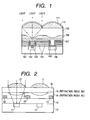
- FIG. 2 is a schematic sectional view showing the first embodiment of the present invention.
- a solid-state image pickup device shown in Fig. 2 has a p- or n-type semiconductor substrate 10, and photoelectric conversion elements 11 formed in the semiconductor substrate 10.
- Each photoelectric conversion element 11 is a region of a conductivity type opposite to that of the substrate 10, and forms a PN diode with the substrate 10.
- a surface passivation layer 12 is formed on the photoelectric conversion elements 11 and the remaining surface of the semiconductor substrate 10.
- Conductive layers 13 are formed on the surface passivation layer on the remaining surface of the semiconductor substrate 10 and, for example, transfer photocharges of the photoelectric conversion elements 11.
- a first interlayer layer 14 is formed on the conductive layers 13 and the surface passivation layer 12.
- a second interlayer layer 15 forms a concave lens on the first interlayer layer 14.
- a resin layer 16 consists of a transparent polymer resin. Convex microlenses 17 are formed on the resin layer 16 at positions above the photoelectric conversion elements 11. In this structure, the respective layers formed above the photoelectric conversion elements 11 are transparent. Light coming from above is condensed to excite electrons and holes in the photoelectric conversion elements 11, and is output to an external circuit as an image signal via the conductive layers 13.
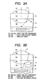
- Figs. 3A and 3B show examples of the refraction indices of the respective layers of the solid-state image pickup device.
- N1 be the refraction index of air
- N2 be that of the convex microlens 17
- N3 be that of the resin layer 16
- N4 be that of the second interlayer layer 15
- N5 be that of the first interlayer layer 14. Then, if these refraction indices are set to satisfy:
- both the first and second interlayer layers may be formed of TEOS (Tetra-Ethyl-Ortho-Silicate)-SiO 2 and have different densities.
- TEOS Tetra-Ethyl-Ortho-Silicate
- the above embodiment has explained a solid-state image pickup device having first and second interlayer layers and microlens.
- the present invention is not limited to such specific device, but may be applied to a solid-state image pickup device that condenses light by a structure with a first interlayer layer alone.
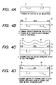
- a solid-state image pickup device of this embodiment is manufactured by the following method.
- a resist mask is formed on a semiconductor substrate 10 except for prospective formation regions of photoelectric conversion elements, and a Group III element such as boron in case of an n-type semiconductor substrate 10 or a Group V element such as phosphorus in case of a p-type semiconductor substrate 10 is ion-implanted to form photoelectric conversion elements 11.
- a Group III element such as boron in case of an n-type semiconductor substrate 10 or a Group V element such as phosphorus in case of a p-type semiconductor substrate 10 is ion-implanted to form photoelectric conversion elements 11.
- an impurity such as silicon, phosphorus, boron, or the like is ionized, and is implanted into a wafer of the semiconductor substrate by applying an appropriate acceleration voltage. After implantation, the wafer is annealed at high temperature to electrically activate the impurity.
- a surface passivation layer 12 as an insulating member is formed on the photoelectric conversion elements 11 and the remaining surface of the semiconductor substrate 10 by LP (Low pressure) CVD, and conductive layers 13 consisting of a metal such as Al or the like and serving as light-shielding layers are formed by sputtering or the like.
- a plurality of conductive layers 13 may be formed via the surface passivation films 12.
- a first interlayer layer 14 having roughly a uniform thickness is formed on the entire surface by TEOS-CVD.
- the first interlayer layer 14 is also formed on the conductive layers 13 on the surface passivation layer 12 to have a uniform thickness, thus providing a concave surface corresponding the heights of the conductive layers 13, which are formed at a predetermined spacing.
- a second interlayer layer 15 having a refraction index different from that of the first interlayer layer 14 is stacked on the first interlayer layer 14.
- a second interlayer layer 15 having a uniform thickness is formed on the entire surface, a concave surface is formed in correspondence with the heights of the conductive layers 13, which are formed at a predetermined spacing.
- a dense TEOS (Tetra-Ethyl-Ortho-Silicate)-SiO 2 layer is formed as the first interlayer layer 14
- a coarse TEOS (Tetra-Ethyl-Ortho-Silicate)-SiO 2 layer is formed as the second interlayer layer 15, the polishing speed by the next CMP can be improved.
- the upper surface is leveled by polishing the entire surface by CMP (Chemical Mechanical Polishing), and the second interlayer layer 15 is polished until downward convex lenses are formed.
- CMP Chemical Mechanical Polishing
- a transparent polymer resin layer 16 is formed, and convex microlenses 17 are formed.
- the transparent polymer resin layer 16 may or may not be formed.
- a color-filter layer may be formed under the microlenses 17.
- a transparent resin layer having a low refraction index may be formed on the convex microlenses 17 so as to level and protect the surface.
- the manufacturing process can be simplified, thus improving the manufacturing yield.
- microlenses can be accurately formed above the photoelectric conversion elements, alignment precision of the microlenses can be improved.
- the downward convex microlenses 15 are formed at positions above the photoelectric conversion elements 11 that form an area sensor and between the neighboring conductive layers 13. Hence, the spacings and heights of the conductive layers 13 are important parameters upon forming the downward convex microlenses 15.
- Fig. 5 is a plan view showing the photoelectric conversion element and its peripheral circuits.
- Fig. 5 illustrates the photoelectric conversion element 11 as a photodiode, one vertical select line 131 of the conductive layers 13, an output signal line 132, a transfer transistor 133, an output signal line 134 in the neighborhood of the output signal line 132, a through hole 135 connected to the source/drain of the transfer transistor 133, and a dummy conductive layer 136.
- the downward convex microlens 15 shown in Fig. 4D are formed on low-level photodiode portions bounded by the output signal lines 132 and 134, vertical select line 131, and dummy conductive layer 136.
- the dummy conductive layer 136 is provided to form a step upon forming the convex microlens 15. If no dummy conductive layer 136 is formed, no conductive layer 13 is formed until the next vertical select line, and the convex microlens 15 cannot be formed.
- a power supply interconnect for the photoelectric conversion element may be formed since the power supply interconnect preferably has constant potential compared to a conductive layer in a floating state.
- the four sides that bound the convex microlens 15 are the conductive layers 13 formed on the surface passivation layer 12 shown in Fig. 4B, and the vertical select line 131 is formed on the output signal lines 132 and 134 to sandwich the surface passivation layer 12 therebetween.
- Fig. 6 is a plan view showing another example of the photoelectric conversion element 11 and its peripheral circuits.
- a light-shielding aperture portion 137 consisting of a metal such as Al or the like is formed around the photoelectric conversion element 11 as a photodiode.
- the light-shielding aperture portion 137 is obtained by forming the light-shielding layer 13 shown in Fig. 4B on the surface passivation layer 12 to have a step, so that it has a height equal to or larger than those of the vertical select line 131 and the output signal lines 132 and 134 as conductive layers around the photoelectric conversion element 11.
- the light-shielding aperture portion 137 may be formed to cover the vertical signal line 131 and output signal lines 132 and 134 to intercept light that becomes incident on a portion other than the photoelectric conversion element 11.
- the shape of the downward convex microlens 15 above the photoelectric conversion element 11 can be clearly distinguished, and the microlens 15 can be formed without any variations in area and height, thus improving the characteristics of the microlens.
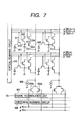
- Fig. 7 is a circuit diagram of a solid-state image pickup device with a microlens.
- Fig. 7 shows the arrangement of a two-dimensional sensor having 2 x 2 pixels, but the number of pixels is not limited to four.
- CMOS area sensor shown in Fig. 7
- a photodiode 901, transfer switch 911, reset switch 902, pixel amplifier 903, and row select switch 904 are formed in each pixel.
- the gate of the transfer switch 911 is connected to ⁇ TX(n or n+1) from a vertical scanning circuit 910
- the gate of the reset switch 902 is connected to ⁇ RES(n or n+1) from the vertical scanning circuit 910
- the gate of the row select switch 904 is connected to ⁇ SEL(n or n+1) from the vertical scanning circuit 910.
- Photoelectric conversion is done by the photodiode 901.
- the transfer switch 911 is kept OFF, and no charge photoelectrically converted by the photodiode 901 is transferred to the gate of a source-follower 903 that constructs the pixel amplifier.
- the gate of the source-follower 903 that constructs the pixel amplifier is reset to an appropriate voltage since the reset switch 902 is turned on before the beginning of accumulation. That is, this reset level corresponds to dark level.
- the row select switch 904 when the row select switch 904 is turned on, the source-follower constituted by a load current source 905 and the pixel amplifier 903 is operative, and when the transfer switch 911 is turned on that timing, the charge accumulated on the photodiode 901 is transferred to the gate of the source-follower constructed by the pixel amplifier.
- the output of the selected row is generated on a vertical output line 906.
- This output is accumulated in a signal accumulation unit 907 via transfer gates 909a and 909b.
- the output temporarily stored in the signal accumulation unit 907 is sequentially read out to an output unit VO by a horizontal scanning circuit 908.
- Fig. 8 is a plan view of the photoelectric conversion element corresponding to Fig. 7.
- the same reference numerals in Fig. 8 denote the same parts as those in Fig. 7.
- each photoelectric conversion element is composed of the photodiode 901, transfer switch 911, source-follower 903, its gate, and the like, and the photodiode 901 is bounded by select lines ⁇ SEL(n or n+1) and ⁇ TX(n or n+1), the vertical output line 906, and a power supply line V DD .
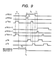
- Fig. 9 is a timing chart showing the operation of the CMOS area sensor shown in Fig. 7.
- T1 At the timing of an all-pixel reset period T1, ⁇ TX(n) and ⁇ T(n+1) are activated, and the charges on the photodiodes 901 of all pixels are transferred to the gates of the corresponding source-follower 903 via the transfer switches 911, thus resetting the photodiodes 901.
- the cathode charges of the photodiodes 901 are transferred to those of the source-followers 903 and are averaged.
- the average level becomes equal to the reset level of the cathode of the photodiode 901.
- a mechanical shutter 11 (not shown) that guides an optical image to be sensed is open, and all the pixels begin to accumulate charges simultaneously with the end of the period T1.
- the mechanical shutter 11 is kept open during a period T3, which corresponds to the accumulation period of the photodiodes 901.
- the mechanical shutter is closed at timing T4, thus ending photocharge accumulation of the photodiodes 901.
- the photodiodes 901 accumulate charges.
- a read is started in units of lines. More specifically, the (N-1)-th row is read out, and then the N-th row is read out.
- ⁇ SEL(n) is activated to turn on the row select switch 904, so that the source-follower circuits constructed by the pixel amplifiers 903 in all pixels connected to the n-th row are rendered operative.
- the gate of the source-follower constructed by the pixel amplifier 903 is reset since ⁇ RES(n) is activated during a period T2 to turn on the reset switch 902. More specifically, this dark-level signal is output onto the vertical output line 906.
- ⁇ TN(n) is activated to turn on the transfer gate 909b, thus holding charges in the signal accumulation unit 907.
- This operation is parallelly executed for all pixels connected to the N-th row.
- signal charges accumulated on the photodiodes 901 are transferred to the gates of the source-followers comprised of the pixel amplifiers 903 by turning on the transfer switches 911 by activating ⁇ TX(n).
- the potential of the gate of each source-follower constructed by the pixel amplifier 903 varies from reset level by an amount corresponding to the transferred signal charge, thus determining the signal level.
- ⁇ TS is activated to turn on the transfer gate 909a, thus holding the signal levels in the signal accumulation unit 907.
- This operation is parallelly executed for all pixels connected to the N-th row.
- the signal accumulation unit 907 holds dark levels and signal levels of all pixels connected to the N-th row, and the difference between the dark and signal levels is calculated in units of pixels to cancel fixed pattern noise (FPN) due to variations of threshold voltages Vth of the source-followers and KTC noise produced upon resetting of the reset switches 902, thereby obtaining high S/N signals from which noise components have been removed.
- FPN fixed pattern noise
- the solid-state image pickup element of this embodiment can be realized by a CMOS compatible process, and can be formed on one chip together with peripheral circuits, low cost and multiple functions can be realized. Furthermore, as downward convex microlens aligned by the output signal line 906, the reset line ⁇ RES as a vertical select line, and the like, can be formed above the photodiode 901, photodetection sensitivity can be greatly improved.
- a solid-state image pickup device having a function of condensing light on the photoelectric conversion element can be formed by a simple manufacturing method, i.e., by forming downward convex microlens in correspondence with the upper convex microlens.
- microlenses are manufactured by bounding the photoelectric conversion elements using a light-shielding layer, a plurality of microlenses can be accurately aligned and formed, thus providing a high-precision, high-density, high-sensitivity solid-state image pickup device suffering less variations.
- the optical axis can be set to agree with the condensed point, thus improving photoelectric conversion efficiency.
Landscapes
- Solid State Image Pick-Up Elements (AREA)
- Transforming Light Signals Into Electric Signals (AREA)
Applications Claiming Priority (2)
| Application Number | Priority Date | Filing Date | Title |
|---|---|---|---|
| JP7053698 | 1998-03-19 | ||
| JP07053698A JP3571909B2 (ja) | 1998-03-19 | 1998-03-19 | 固体撮像装置及びその製造方法 |
Publications (3)
| Publication Number | Publication Date |
|---|---|
| EP0948055A2 true EP0948055A2 (de) | 1999-10-06 |
| EP0948055A3 EP0948055A3 (de) | 2000-09-27 |
| EP0948055B1 EP0948055B1 (de) | 2007-04-11 |
Family
ID=13434366
Family Applications (1)
| Application Number | Title | Priority Date | Filing Date |
|---|---|---|---|
| EP99302092A Expired - Lifetime EP0948055B1 (de) | 1998-03-19 | 1999-03-18 | Festkörper-Bildaufnahmevorrichtung |
Country Status (4)
| Country | Link |
|---|---|
| US (2) | US6188094B1 (de) |
| EP (1) | EP0948055B1 (de) |
| JP (1) | JP3571909B2 (de) |
| DE (1) | DE69935751D1 (de) |
Cited By (11)
| Publication number | Priority date | Publication date | Assignee | Title |
|---|---|---|---|---|
| US6586811B2 (en) | 2000-04-07 | 2003-07-01 | Canon Kabushiki Kaisha | Microlens, solid state imaging device, and production process thereof |
| EP1367650A1 (de) * | 2002-05-27 | 2003-12-03 | STMicroelectronics S.A. | Elektronische Vorrichtung mit elektronischen Schaltungen und einer photosensitiven Zone und deren Verfahren zur Herstellung |
| WO2004030101A1 (ja) * | 2002-09-27 | 2004-04-08 | Sony Corporation | 固体撮像素子及びその製造方法 |
| EP1414074A3 (de) * | 2002-10-25 | 2005-07-06 | OmniVision International Holding Ltd | Bildsensor mit Farbfiltern mit reduzierter Verspannung und Herstellungsverfahren |
| EP1339225A3 (de) * | 2002-02-21 | 2005-07-13 | Canon Kabushiki Kaisha | Abbildungsvorrichtung |
| EP1414070A3 (de) * | 2002-10-25 | 2005-08-10 | OmniVision International Holding Ltd | Bildsensor mit konkav geformten Mirkolinsen |
| EP1414071A3 (de) * | 2002-10-25 | 2005-08-24 | OmniVision International Holding Ltd | Verfahren zur Herstellung eines Bildsensors mit konkav geformten Mikrolinsen |
| EP1414073A3 (de) * | 2002-10-25 | 2005-09-21 | OmniVision International Holding Ltd | Bildsensor mit Mikrolinsen mit integrierten Farbfiltern und dessen Verfahren zur Herstellung |
| WO2009158105A3 (en) * | 2008-06-25 | 2010-03-04 | Aptina Imaging Corporation | Imaging module with symmetrical lens system and method of manufacture |
| EP2487716A3 (de) * | 2011-02-09 | 2013-05-15 | Canon Kabushiki Kaisha | Festkörper-Bildaufnahmevorrichtung und Ansteuerungsverfahren dafür |
| WO2019199602A1 (en) * | 2018-04-10 | 2019-10-17 | Nthdegree Technologies Worldwide Inc. | Self-alignment of optical structures to random array of printed micro-leds |
Families Citing this family (141)
| Publication number | Priority date | Publication date | Assignee | Title |
|---|---|---|---|---|
| JP3620237B2 (ja) * | 1997-09-29 | 2005-02-16 | ソニー株式会社 | 固体撮像素子 |
| US20080128844A1 (en) * | 2002-11-18 | 2008-06-05 | Tessera North America | Integrated micro-optical systems and cameras including the same |
| US6426829B1 (en) * | 1998-03-26 | 2002-07-30 | Digital Optics Corp. | Integrated micro-optical systems |
| US6083429A (en) * | 1998-03-31 | 2000-07-04 | Intel Corporation | Microlens formation through focal plane control of a aerial image |
| JP4200545B2 (ja) * | 1998-06-08 | 2008-12-24 | ソニー株式会社 | 固体撮像素子およびその駆動方法、並びにカメラシステム |
| US6583438B1 (en) * | 1999-04-12 | 2003-06-24 | Matsushita Electric Industrial Co., Ltd. | Solid-state imaging device |
| JP4265038B2 (ja) * | 1999-08-02 | 2009-05-20 | ソニー株式会社 | 画像処理装置 |
| EP1091409B1 (de) * | 1999-10-05 | 2010-08-18 | Canon Kabushiki Kaisha | Festkörperbildaufnahmevorrichtung und Bildaufnahmesystem |
| US7324144B1 (en) | 1999-10-05 | 2008-01-29 | Canon Kabushiki Kaisha | Solid image pickup device, image pickup system and method of driving solid image pickup device |
| JP3296345B2 (ja) * | 1999-11-04 | 2002-06-24 | 日本電気株式会社 | 固体撮像装置及びその製造方法 |
| JP3467013B2 (ja) | 1999-12-06 | 2003-11-17 | キヤノン株式会社 | 固体撮像装置 |
| JP4845247B2 (ja) * | 1999-12-27 | 2011-12-28 | キヤノン株式会社 | 光電変換装置 |
| JP4123667B2 (ja) * | 2000-01-26 | 2008-07-23 | 凸版印刷株式会社 | 固体撮像素子の製造方法 |
| US6960817B2 (en) | 2000-04-21 | 2005-11-01 | Canon Kabushiki Kaisha | Solid-state imaging device |
| US6514785B1 (en) * | 2000-06-09 | 2003-02-04 | Taiwan Semiconductor Manufacturing Company | CMOS image sensor n-type pin-diode structure |
| US6653617B2 (en) | 2000-07-03 | 2003-11-25 | Canon Kabushiki Kaisha | Photoelectric conversion device |
| US6541794B1 (en) * | 2000-08-31 | 2003-04-01 | Motorola, Inc. | Imaging device and method |
| KR100477784B1 (ko) * | 2000-08-31 | 2005-03-22 | 매그나칩 반도체 유한회사 | 트렌치 내부의 공기로 이루어지는 집광층을 구비하는이미지 센서 및 그 제조 방법 |
| JP2002252338A (ja) * | 2000-12-18 | 2002-09-06 | Canon Inc | 撮像装置及び撮像システム |
| US6855937B2 (en) * | 2001-05-18 | 2005-02-15 | Canon Kabushiki Kaisha | Image pickup apparatus |
| US6566151B2 (en) * | 2001-06-21 | 2003-05-20 | United Microelectronics Corp. | Method of forming a color filter |
| US20020196553A1 (en) * | 2001-06-26 | 2002-12-26 | Colandene Thomas M. | Off-focal plane micro-optics |
| JP4224963B2 (ja) * | 2001-10-26 | 2009-02-18 | オムロン株式会社 | レンズアレイ基板及び液晶表示装置 |
| KR100399971B1 (ko) * | 2001-11-06 | 2003-09-29 | 주식회사 하이닉스반도체 | 이미지 센서 및 그 제조방법 |
| US6730914B2 (en) * | 2002-02-05 | 2004-05-04 | E-Phocus, Inc. | Photoconductor-on-active-pixel (POAP) sensor utilizing equal-potential pixel electrodes |
| US6798033B2 (en) * | 2002-08-27 | 2004-09-28 | E-Phocus, Inc. | Photoconductor-on-active-pixel (POAP) sensor utilizing a multi-layered radiation absorbing structure |
| JP2003229553A (ja) * | 2002-02-05 | 2003-08-15 | Sharp Corp | 半導体装置及びその製造方法 |
| EP1341377B1 (de) | 2002-02-27 | 2018-04-11 | Canon Kabushiki Kaisha | Signalverarbeitungsvorrichtung für Bildaufnahmevorrichtung |
| JP4262446B2 (ja) * | 2002-06-21 | 2009-05-13 | 富士フイルム株式会社 | 固体撮像装置 |
| KR100873289B1 (ko) * | 2002-07-19 | 2008-12-11 | 매그나칩 반도체 유한회사 | 경사입사광의 영향을 감소시킨 시모스 이미지센서 |
| US8059345B2 (en) * | 2002-07-29 | 2011-11-15 | Digitaloptics Corporation East | Integrated micro-optical systems |
| US6737719B1 (en) * | 2002-10-25 | 2004-05-18 | Omnivision International Holding Ltd | Image sensor having combination color filter and concave-shaped micro-lenses |
| US6803250B1 (en) * | 2003-04-24 | 2004-10-12 | Taiwan Semiconductor Manufacturing Co., Ltd | Image sensor with complementary concave and convex lens layers and method for fabrication thereof |
| JP4274533B2 (ja) * | 2003-07-16 | 2009-06-10 | キヤノン株式会社 | 固体撮像装置及びその駆動方法 |
| US20050045927A1 (en) * | 2003-09-03 | 2005-03-03 | Jin Li | Microlenses for imaging devices |
| US7408195B2 (en) * | 2003-09-04 | 2008-08-05 | Cypress Semiconductor Corporation (Belgium) Bvba | Semiconductor pixel arrays with reduced sensitivity to defects |
| US7115853B2 (en) * | 2003-09-23 | 2006-10-03 | Micron Technology, Inc. | Micro-lens configuration for small lens focusing in digital imaging devices |
| KR100549589B1 (ko) * | 2003-09-29 | 2006-02-08 | 매그나칩 반도체 유한회사 | 이미지센서 및 그 제조 방법 |
| US7227692B2 (en) * | 2003-10-09 | 2007-06-05 | Micron Technology, Inc | Method and apparatus for balancing color response of imagers |
| US7560295B2 (en) * | 2003-10-09 | 2009-07-14 | Aptina Imaging Corporation | Methods for creating gapless inner microlenses, arrays of microlenses, and imagers having same |
| JP4514188B2 (ja) | 2003-11-10 | 2010-07-28 | キヤノン株式会社 | 光電変換装置及び撮像装置 |
| FR2862426B1 (fr) * | 2003-11-17 | 2006-03-03 | St Microelectronics Sa | Capteur d'image |
| JP4508619B2 (ja) * | 2003-12-03 | 2010-07-21 | キヤノン株式会社 | 固体撮像装置の製造方法 |
| JP3793202B2 (ja) * | 2004-02-02 | 2006-07-05 | キヤノン株式会社 | 固体撮像装置 |
| JP3890333B2 (ja) * | 2004-02-06 | 2007-03-07 | キヤノン株式会社 | 固体撮像装置 |
| JP4067054B2 (ja) * | 2004-02-13 | 2008-03-26 | キヤノン株式会社 | 固体撮像装置および撮像システム |
| US7423790B2 (en) * | 2004-03-18 | 2008-09-09 | Canon Kabushiki Kaisha | Photoelectric conversion apparatus and contact-type image sensor |
| JP4553612B2 (ja) * | 2004-03-18 | 2010-09-29 | ルネサスエレクトロニクス株式会社 | 撮像素子およびそれを備えた撮像装置 |
| US7372497B2 (en) * | 2004-04-28 | 2008-05-13 | Taiwan Semiconductor Manufacturing Company | Effective method to improve sub-micron color filter sensitivity |
| KR100640972B1 (ko) * | 2004-07-15 | 2006-11-02 | 동부일렉트로닉스 주식회사 | 씨모스 이미지 센서 및 그의 제조 방법 |
| DE602005025834D1 (de) * | 2004-08-13 | 2011-02-24 | St Microelectronics Sa | Bildsensor |
| JP5089017B2 (ja) * | 2004-09-01 | 2012-12-05 | キヤノン株式会社 | 固体撮像装置及び固体撮像システム |
| JP4756839B2 (ja) | 2004-09-01 | 2011-08-24 | キヤノン株式会社 | 固体撮像装置及びカメラ |
| JP4971586B2 (ja) * | 2004-09-01 | 2012-07-11 | キヤノン株式会社 | 固体撮像装置 |
| US20060057765A1 (en) * | 2004-09-13 | 2006-03-16 | Taiwan Semiconductor Manufacturing Company, Ltd. | Image sensor including multiple lenses and method of manufacture thereof |
| US7768088B2 (en) * | 2004-09-24 | 2010-08-03 | Fujifilm Corporation | Solid-state imaging device that efficiently guides light to a light-receiving part |
| US7389013B2 (en) * | 2004-09-30 | 2008-06-17 | Stmicroelectronics, Inc. | Method and system for vertical optical coupling on semiconductor substrate |
| US20060071149A1 (en) * | 2004-09-30 | 2006-04-06 | Stmicroelectronics, Inc. | Microlens structure for opto-electric semiconductor device, and method of manufacture |
| JP4513497B2 (ja) * | 2004-10-19 | 2010-07-28 | ソニー株式会社 | 固体撮像装置 |
| US7420610B2 (en) * | 2004-12-15 | 2008-09-02 | Matsushita Electric Industrial Co., Ltd. | Solid-state imaging element, solid-state imaging device, and method for fabricating the same |
| KR100672702B1 (ko) * | 2004-12-29 | 2007-01-22 | 동부일렉트로닉스 주식회사 | 씨모스 이미지 센서 및 그 제조방법 |
| JP4459064B2 (ja) * | 2005-01-14 | 2010-04-28 | キヤノン株式会社 | 固体撮像装置、その制御方法及びカメラ |
| JP4416668B2 (ja) * | 2005-01-14 | 2010-02-17 | キヤノン株式会社 | 固体撮像装置、その制御方法及びカメラ |
| JP2006197392A (ja) * | 2005-01-14 | 2006-07-27 | Canon Inc | 固体撮像装置、カメラ、及び固体撮像装置の駆動方法 |
| JP4549195B2 (ja) | 2005-01-19 | 2010-09-22 | キヤノン株式会社 | 固体撮像素子およびその製造方法 |
| JP4508891B2 (ja) * | 2005-01-28 | 2010-07-21 | キヤノン株式会社 | 光電変換装置、マルチチップ型イメージセンサ、密着型イメージセンサおよび画像読取装置 |
| JP4434991B2 (ja) * | 2005-03-01 | 2010-03-17 | キヤノン株式会社 | イメージセンサ |
| JP4459099B2 (ja) * | 2005-03-18 | 2010-04-28 | キヤノン株式会社 | 固体撮像装置及びカメラ |
| JP4677258B2 (ja) | 2005-03-18 | 2011-04-27 | キヤノン株式会社 | 固体撮像装置及びカメラ |
| JP4459098B2 (ja) * | 2005-03-18 | 2010-04-28 | キヤノン株式会社 | 固体撮像装置及びカメラ |
| JP4794877B2 (ja) * | 2005-03-18 | 2011-10-19 | キヤノン株式会社 | 固体撮像装置及びカメラ |
| US7553689B2 (en) * | 2005-07-13 | 2009-06-30 | Taiwan Semiconductor Manufacturing Co., Ltd. | Semiconductor device with micro-lens and method of making the same |
| JP4469781B2 (ja) * | 2005-07-20 | 2010-05-26 | パナソニック株式会社 | 固体撮像装置及びその製造方法 |
| JP4835080B2 (ja) * | 2005-09-22 | 2011-12-14 | ソニー株式会社 | 固体撮像素子の製造方法、及び、固体撮像素子 |
| US7999291B2 (en) | 2005-09-05 | 2011-08-16 | Sony Corporation | Method of manufacturing solid state imaging device, solid state imaging device, and camera using solid state imaging device |
| JP4967291B2 (ja) * | 2005-09-22 | 2012-07-04 | ソニー株式会社 | 固体撮像装置の製造方法 |
| JP2007201091A (ja) * | 2006-01-25 | 2007-08-09 | Fujifilm Corp | 固体撮像素子の製造方法 |
| JP2007242697A (ja) * | 2006-03-06 | 2007-09-20 | Canon Inc | 撮像装置および撮像システム |
| KR101255334B1 (ko) * | 2006-05-08 | 2013-04-16 | 페어차일드코리아반도체 주식회사 | 저 열저항 파워 모듈 및 그 제조방법 |
| KR100795922B1 (ko) * | 2006-07-28 | 2008-01-21 | 삼성전자주식회사 | 이미지 픽업 소자 및 이미지 픽업 소자의 제조방법 |
| JP4185949B2 (ja) * | 2006-08-08 | 2008-11-26 | キヤノン株式会社 | 光電変換装置及び撮像装置 |
| JP4928199B2 (ja) * | 2006-09-07 | 2012-05-09 | キヤノン株式会社 | 信号検出装置、信号検出装置の信号読み出し方法及び信号検出装置を用いた撮像システム |
| US20080191299A1 (en) * | 2007-02-12 | 2008-08-14 | Christopher Parks | Microlenses for irregular pixels |
| JP4054839B1 (ja) | 2007-03-02 | 2008-03-05 | キヤノン株式会社 | 光電変換装置およびそれを用いた撮像システム |
| US9019830B2 (en) * | 2007-05-15 | 2015-04-28 | Imagine Communications Corp. | Content-based routing of information content |
| JP5180537B2 (ja) * | 2007-08-24 | 2013-04-10 | キヤノン株式会社 | 光電変換装置及びマルチチップイメージセンサ |
| EP2037667B1 (de) * | 2007-09-14 | 2017-08-23 | Canon Kabushiki Kaisha | Bildabtastvorrichtung und Bildgebungssystem |
| US8395686B2 (en) * | 2007-12-06 | 2013-03-12 | Sony Corporation | Solid-state imaging device, method of manufacturing the same, and camera |
| JP5142696B2 (ja) | 2007-12-20 | 2013-02-13 | キヤノン株式会社 | 光電変換装置、及び光電変換装置を用いた撮像システム |
| KR100967477B1 (ko) * | 2007-12-24 | 2010-07-07 | 주식회사 동부하이텍 | 이미지 센서 및 그 제조 방법 |
| JP5268389B2 (ja) * | 2008-02-28 | 2013-08-21 | キヤノン株式会社 | 固体撮像装置、その駆動方法及び撮像システム |
| JP5178266B2 (ja) * | 2008-03-19 | 2013-04-10 | キヤノン株式会社 | 固体撮像装置 |
| JP5094498B2 (ja) | 2008-03-27 | 2012-12-12 | キヤノン株式会社 | 固体撮像装置及び撮像システム |
| JP5328207B2 (ja) * | 2008-04-01 | 2013-10-30 | キヤノン株式会社 | 固体撮像装置 |
| JP2009252983A (ja) * | 2008-04-04 | 2009-10-29 | Canon Inc | 撮像センサー、及び撮像センサーの製造方法 |
| JP5086877B2 (ja) * | 2008-04-11 | 2012-11-28 | シャープ株式会社 | 固体撮像素子およびその製造方法、電子情報機器 |
| JP5274166B2 (ja) * | 2008-09-10 | 2013-08-28 | キヤノン株式会社 | 光電変換装置及び撮像システム |
| JP5478905B2 (ja) * | 2009-01-30 | 2014-04-23 | キヤノン株式会社 | 固体撮像装置 |
| JP2010239076A (ja) * | 2009-03-31 | 2010-10-21 | Sony Corp | 固体撮像装置とその製造方法、及び電子機器 |
| JP2010251489A (ja) * | 2009-04-15 | 2010-11-04 | Sony Corp | 固体撮像装置および電子機器 |
| JP5529613B2 (ja) * | 2009-04-17 | 2014-06-25 | キヤノン株式会社 | 光電変換装置及び撮像システム |
| JP2009296016A (ja) * | 2009-09-18 | 2009-12-17 | Renesas Technology Corp | 固体撮像素子 |
| JP5556122B2 (ja) * | 2009-10-27 | 2014-07-23 | ソニー株式会社 | 固体撮像装置、固体撮像装置の製造方法、電子機器 |
| JP2011100900A (ja) | 2009-11-06 | 2011-05-19 | Sony Corp | 固体撮像装置及びその製造方法と設計方法並びに電子機器 |
| JP5679653B2 (ja) | 2009-12-09 | 2015-03-04 | キヤノン株式会社 | 光電変換装置およびそれを用いた撮像システム |
| JP5780711B2 (ja) | 2010-04-06 | 2015-09-16 | キヤノン株式会社 | 固体撮像装置 |
| JP2012084815A (ja) * | 2010-10-14 | 2012-04-26 | Sharp Corp | 固体撮像装置および電子情報機器 |
| JP5736755B2 (ja) * | 2010-12-09 | 2015-06-17 | ソニー株式会社 | 固体撮像装置とその製造方法、及び電子機器 |
| JP5744545B2 (ja) * | 2011-01-31 | 2015-07-08 | キヤノン株式会社 | 固体撮像装置およびカメラ |
| JP6045136B2 (ja) | 2011-01-31 | 2016-12-14 | キヤノン株式会社 | 光電変換装置 |
| JP5901186B2 (ja) | 2011-09-05 | 2016-04-06 | キヤノン株式会社 | 固体撮像装置及びその駆動方法 |
| JP5858695B2 (ja) | 2011-09-08 | 2016-02-10 | キヤノン株式会社 | 固体撮像装置及び固体撮像装置の駆動方法 |
| JP5806566B2 (ja) | 2011-09-15 | 2015-11-10 | キヤノン株式会社 | A/d変換器および固体撮像装置 |
| JP5801665B2 (ja) | 2011-09-15 | 2015-10-28 | キヤノン株式会社 | 固体撮像装置、a/d変換器およびその制御方法 |
| JP5930651B2 (ja) | 2011-10-07 | 2016-06-08 | キヤノン株式会社 | 固体撮像装置 |
| JP5901212B2 (ja) | 2011-10-07 | 2016-04-06 | キヤノン株式会社 | 光電変換システム |
| JP5484422B2 (ja) | 2011-10-07 | 2014-05-07 | キヤノン株式会社 | 固体撮像装置 |
| CN103066090B (zh) * | 2012-12-26 | 2017-11-07 | 上海集成电路研发中心有限公司 | 具有凸透镜结构的像元结构及制造方法 |
| JP6319946B2 (ja) | 2013-04-18 | 2018-05-09 | キヤノン株式会社 | 固体撮像装置及び撮像システム |
| JP6100074B2 (ja) | 2013-04-25 | 2017-03-22 | キヤノン株式会社 | 光電変換装置及び撮像システム |
| JP6274788B2 (ja) | 2013-08-28 | 2018-02-07 | キヤノン株式会社 | 撮像装置、撮像システム及び撮像装置の駆動方法 |
| JP5886806B2 (ja) | 2013-09-17 | 2016-03-16 | キヤノン株式会社 | 固体撮像装置 |
| JP6207351B2 (ja) | 2013-11-12 | 2017-10-04 | キヤノン株式会社 | 固体撮像装置および撮像システム |
| JP6239975B2 (ja) | 2013-12-27 | 2017-11-29 | キヤノン株式会社 | 固体撮像装置及びそれを用いた撮像システム |
| JP6541347B2 (ja) | 2014-03-27 | 2019-07-10 | キヤノン株式会社 | 固体撮像装置および撮像システム |
| JP6548391B2 (ja) | 2014-03-31 | 2019-07-24 | キヤノン株式会社 | 光電変換装置および撮像システム |
| JP6412328B2 (ja) | 2014-04-01 | 2018-10-24 | キヤノン株式会社 | 固体撮像装置およびカメラ |
| US9979916B2 (en) | 2014-11-21 | 2018-05-22 | Canon Kabushiki Kaisha | Imaging apparatus and imaging system |
| KR102372856B1 (ko) * | 2014-11-28 | 2022-03-10 | 엘지전자 주식회사 | 마이크로 렌즈 어레이를 구비하는 광 검출 센서 |
| US9900539B2 (en) | 2015-09-10 | 2018-02-20 | Canon Kabushiki Kaisha | Solid-state image pickup element, and image pickup system |
| JP6703387B2 (ja) * | 2015-10-02 | 2020-06-03 | エルジー ディスプレイ カンパニー リミテッド | 薄膜光センサ、2次元アレイセンサ、および指紋センサ付きモバイル用ディスプレイ |
| JP6740067B2 (ja) | 2016-09-16 | 2020-08-12 | キヤノン株式会社 | 固体撮像装置及びその駆動方法 |
| JP6750876B2 (ja) | 2016-10-07 | 2020-09-02 | キヤノン株式会社 | 固体撮像装置及びその駆動方法 |
| JP2018082261A (ja) | 2016-11-15 | 2018-05-24 | キヤノン株式会社 | 撮像素子 |
| JP6806553B2 (ja) | 2016-12-15 | 2021-01-06 | キヤノン株式会社 | 撮像装置、撮像装置の駆動方法及び撮像システム |
| JP6871797B2 (ja) | 2017-04-24 | 2021-05-12 | キヤノン株式会社 | 光電変換装置 |
| JP7299680B2 (ja) | 2018-08-23 | 2023-06-28 | キヤノン株式会社 | 撮像装置及び撮像システム |
| JP7245014B2 (ja) * | 2018-09-10 | 2023-03-23 | キヤノン株式会社 | 固体撮像装置、撮像システム、および固体撮像装置の駆動方法 |
| US11425365B2 (en) | 2018-12-14 | 2022-08-23 | Canon Kabushiki Kaisha | Photoelectric conversion device, method of manufacturing photoelectric conversion device, and method of manufacturing semiconductor device |
| JP7558777B2 (ja) * | 2020-12-02 | 2024-10-01 | シャープ福山レーザー株式会社 | 画像表示素子 |
| US20240377580A1 (en) * | 2023-05-11 | 2024-11-14 | Taiwan Semiconductor Manufacturing Co., Ltd. | Optical device and methods of manufacture |
Family Cites Families (14)
| Publication number | Priority date | Publication date | Assignee | Title |
|---|---|---|---|---|
| US5118924A (en) * | 1990-10-01 | 1992-06-02 | Eastman Kodak Company | Static control overlayers on opto-electronic devices |
| JP2558389B2 (ja) * | 1990-11-29 | 1996-11-27 | 松下電器産業株式会社 | 固体撮像装置 |
| JP3200856B2 (ja) * | 1991-02-12 | 2001-08-20 | ソニー株式会社 | 固体撮像装置 |
| JP2833941B2 (ja) * | 1992-10-09 | 1998-12-09 | 三菱電機株式会社 | 固体撮像装置とその製造方法 |
| JPH06232379A (ja) * | 1993-02-01 | 1994-08-19 | Sharp Corp | 固体撮像素子 |
| JP2950714B2 (ja) * | 1993-09-28 | 1999-09-20 | シャープ株式会社 | 固体撮像装置およびその製造方法 |
| US5644123A (en) * | 1994-12-16 | 1997-07-01 | Rocky Mountain Research Center | Photonic signal processing, amplification, and computing using special interference |
| US5739548A (en) * | 1995-05-02 | 1998-04-14 | Matsushita Electronics Corporation | Solid state imaging device having a flattening layer and optical lenses |
| JP3405620B2 (ja) * | 1995-05-22 | 2003-05-12 | 松下電器産業株式会社 | 固体撮像装置 |
| JP3031606B2 (ja) * | 1995-08-02 | 2000-04-10 | キヤノン株式会社 | 固体撮像装置と画像撮像装置 |
| US5693967A (en) * | 1995-08-10 | 1997-12-02 | Lg Semicon Co., Ltd. | Charge coupled device with microlens |
| JPH0964325A (ja) | 1995-08-23 | 1997-03-07 | Sony Corp | 固体撮像素子とその製造方法 |
| KR100278285B1 (ko) * | 1998-02-28 | 2001-01-15 | 김영환 | 씨모스 이미지센서 및 그 제조방법 |
| JP4109743B2 (ja) * | 1998-03-19 | 2008-07-02 | 株式会社東芝 | 固体撮像装置 |
-
1998
- 1998-03-19 JP JP07053698A patent/JP3571909B2/ja not_active Expired - Fee Related
-
1999
- 1999-03-16 US US09/270,008 patent/US6188094B1/en not_active Expired - Lifetime
- 1999-03-18 EP EP99302092A patent/EP0948055B1/de not_active Expired - Lifetime
- 1999-03-18 DE DE69935751T patent/DE69935751D1/de not_active Expired - Lifetime
-
2000
- 2000-11-07 US US09/706,860 patent/US6605850B1/en not_active Expired - Lifetime
Cited By (16)
| Publication number | Priority date | Publication date | Assignee | Title |
|---|---|---|---|---|
| US6586811B2 (en) | 2000-04-07 | 2003-07-01 | Canon Kabushiki Kaisha | Microlens, solid state imaging device, and production process thereof |
| US7250973B2 (en) | 2002-02-21 | 2007-07-31 | Canon Kabushiki Kaisha | Image pickup apparatus for reflecting light at an area between successive refractive areas |
| EP1339225A3 (de) * | 2002-02-21 | 2005-07-13 | Canon Kabushiki Kaisha | Abbildungsvorrichtung |
| EP1367650A1 (de) * | 2002-05-27 | 2003-12-03 | STMicroelectronics S.A. | Elektronische Vorrichtung mit elektronischen Schaltungen und einer photosensitiven Zone und deren Verfahren zur Herstellung |
| WO2004030101A1 (ja) * | 2002-09-27 | 2004-04-08 | Sony Corporation | 固体撮像素子及びその製造方法 |
| EP1414070A3 (de) * | 2002-10-25 | 2005-08-10 | OmniVision International Holding Ltd | Bildsensor mit konkav geformten Mirkolinsen |
| EP1414071A3 (de) * | 2002-10-25 | 2005-08-24 | OmniVision International Holding Ltd | Verfahren zur Herstellung eines Bildsensors mit konkav geformten Mikrolinsen |
| EP1414073A3 (de) * | 2002-10-25 | 2005-09-21 | OmniVision International Holding Ltd | Bildsensor mit Mikrolinsen mit integrierten Farbfiltern und dessen Verfahren zur Herstellung |
| EP1414074A3 (de) * | 2002-10-25 | 2005-07-06 | OmniVision International Holding Ltd | Bildsensor mit Farbfiltern mit reduzierter Verspannung und Herstellungsverfahren |
| WO2009158105A3 (en) * | 2008-06-25 | 2010-03-04 | Aptina Imaging Corporation | Imaging module with symmetrical lens system and method of manufacture |
| US7710667B2 (en) | 2008-06-25 | 2010-05-04 | Aptina Imaging Corp. | Imaging module with symmetrical lens system and method of manufacture |
| EP2487716A3 (de) * | 2011-02-09 | 2013-05-15 | Canon Kabushiki Kaisha | Festkörper-Bildaufnahmevorrichtung und Ansteuerungsverfahren dafür |
| US9029967B2 (en) | 2011-02-09 | 2015-05-12 | Canon Kabushiki Kaisha | Solid-state image pickup device having waveguides in light-receiving and light-shielding areas |
| US9577003B2 (en) | 2011-02-09 | 2017-02-21 | Canon Kabushiki Kaisha | Method of forming an image pickup device having two waveguides and a light-shielding member |
| US10615204B2 (en) | 2011-02-09 | 2020-04-07 | Canon Kabushiki Kaisha | Solid-state image pickup device and method of making the same |
| WO2019199602A1 (en) * | 2018-04-10 | 2019-10-17 | Nthdegree Technologies Worldwide Inc. | Self-alignment of optical structures to random array of printed micro-leds |
Also Published As
| Publication number | Publication date |
|---|---|
| US6605850B1 (en) | 2003-08-12 |
| JP3571909B2 (ja) | 2004-09-29 |
| EP0948055B1 (de) | 2007-04-11 |
| EP0948055A3 (de) | 2000-09-27 |
| JPH11274443A (ja) | 1999-10-08 |
| US6188094B1 (en) | 2001-02-13 |
| DE69935751D1 (de) | 2007-05-24 |
Similar Documents
| Publication | Publication Date | Title |
|---|---|---|
| US6605850B1 (en) | Solid-state image pickup device using layers having different refractive indices | |
| US11843015B2 (en) | Image sensors | |
| US12294797B2 (en) | Image sensors including phase detection pixel | |
| KR101893325B1 (ko) | 고체 촬상 장치와 그 제조 방법, 및 전자 기기 | |
| EP1365581B1 (de) | Bildaufnahmegerät | |
| US7335963B2 (en) | Light block for pixel arrays | |
| US8670053B2 (en) | Solid-state imaging device, manufacturing method of solid-state imaging device and electronic apparatus | |
| US11688749B2 (en) | Image sensing device | |
| KR20080089436A (ko) | 이미저의 리세스 영역에 균일 컬러 필터를 제공하는 방법및 장치 | |
| KR20060108378A (ko) | 3차원 구조를 갖는 이미지 센서의 분리형 단위화소 및 그제조방법 | |
| KR20050057378A (ko) | 고체촬상장치 및 그 제조방법 | |
| US7875840B2 (en) | Imager device with anti-fuse pixels and recessed color filter array | |
| JP2001094086A (ja) | 光電変換装置及びその製造方法 | |
| US11742368B2 (en) | Image sensing device and method for forming the same | |
| US20090160001A1 (en) | Image sensor and method for manufacturing the sensor | |
| JP2004134790A (ja) | 固体撮像装置及びその製造方法並びに電子機器 | |
| US12557422B2 (en) | Image sensor | |
| US20240186348A1 (en) | Image sensor | |
| KR20060072172A (ko) | 높은 광 감도를 가지는 이미지 센서 및 그 제조 방법 | |
| KR100769563B1 (ko) | 누설 전류를 감소시킨 이미지 센서 | |
| US20240072086A1 (en) | Image sensing device | |
| KR20060020852A (ko) | 시모스 이미지센서 및 그의 제조방법 |
Legal Events
| Date | Code | Title | Description |
|---|---|---|---|
| PUAI | Public reference made under article 153(3) epc to a published international application that has entered the european phase |
Free format text: ORIGINAL CODE: 0009012 |
|
| AK | Designated contracting states |
Kind code of ref document: A2 Designated state(s): DE FR GB IT NL |
|
| AX | Request for extension of the european patent |
Free format text: AL;LT;LV;MK;RO;SI |
|
| PUAL | Search report despatched |
Free format text: ORIGINAL CODE: 0009013 |
|
| AK | Designated contracting states |
Kind code of ref document: A3 Designated state(s): AT BE CH CY DE DK ES FI FR GB GR IE IT LI LU MC NL PT SE |
|
| AX | Request for extension of the european patent |
Free format text: AL;LT;LV;MK;RO;SI |
|
| 17P | Request for examination filed |
Effective date: 20010219 |
|
| AKX | Designation fees paid |
Free format text: DE FR GB IT NL |
|
| 17Q | First examination report despatched |
Effective date: 20040825 |
|
| GRAP | Despatch of communication of intention to grant a patent |
Free format text: ORIGINAL CODE: EPIDOSNIGR1 |
|
| GRAS | Grant fee paid |
Free format text: ORIGINAL CODE: EPIDOSNIGR3 |
|
| GRAA | (expected) grant |
Free format text: ORIGINAL CODE: 0009210 |
|
| AK | Designated contracting states |
Kind code of ref document: B1 Designated state(s): DE FR GB IT NL |
|
| REG | Reference to a national code |
Ref country code: GB Ref legal event code: FG4D |
|
| REF | Corresponds to: |
Ref document number: 69935751 Country of ref document: DE Date of ref document: 20070524 Kind code of ref document: P |
|
| NLV1 | Nl: lapsed or annulled due to failure to fulfill the requirements of art. 29p and 29m of the patents act | ||
| EN | Fr: translation not filed | ||
| PG25 | Lapsed in a contracting state [announced via postgrant information from national office to epo] |
Ref country code: NL Free format text: LAPSE BECAUSE OF FAILURE TO SUBMIT A TRANSLATION OF THE DESCRIPTION OR TO PAY THE FEE WITHIN THE PRESCRIBED TIME-LIMIT Effective date: 20070411 |
|
| PLBE | No opposition filed within time limit |
Free format text: ORIGINAL CODE: 0009261 |
|
| STAA | Information on the status of an ep patent application or granted ep patent |
Free format text: STATUS: NO OPPOSITION FILED WITHIN TIME LIMIT |
|
| 26N | No opposition filed |
Effective date: 20080114 |
|
| PG25 | Lapsed in a contracting state [announced via postgrant information from national office to epo] |
Ref country code: IT Free format text: LAPSE BECAUSE OF FAILURE TO SUBMIT A TRANSLATION OF THE DESCRIPTION OR TO PAY THE FEE WITHIN THE PRESCRIBED TIME-LIMIT Effective date: 20070411 Ref country code: FR Free format text: LAPSE BECAUSE OF FAILURE TO SUBMIT A TRANSLATION OF THE DESCRIPTION OR TO PAY THE FEE WITHIN THE PRESCRIBED TIME-LIMIT Effective date: 20071207 Ref country code: DE Free format text: LAPSE BECAUSE OF FAILURE TO SUBMIT A TRANSLATION OF THE DESCRIPTION OR TO PAY THE FEE WITHIN THE PRESCRIBED TIME-LIMIT Effective date: 20070712 |
|
| PG25 | Lapsed in a contracting state [announced via postgrant information from national office to epo] |
Ref country code: FR Free format text: LAPSE BECAUSE OF FAILURE TO SUBMIT A TRANSLATION OF THE DESCRIPTION OR TO PAY THE FEE WITHIN THE PRESCRIBED TIME-LIMIT Effective date: 20070411 |
|
| PGFP | Annual fee paid to national office [announced via postgrant information from national office to epo] |
Ref country code: GB Payment date: 20170322 Year of fee payment: 19 |
|
| GBPC | Gb: european patent ceased through non-payment of renewal fee |
Effective date: 20180318 |
|
| PG25 | Lapsed in a contracting state [announced via postgrant information from national office to epo] |
Ref country code: GB Free format text: LAPSE BECAUSE OF NON-PAYMENT OF DUE FEES Effective date: 20180318 |