EP0948127A1 - Améliorations de ou en relation avec des circuits intégrés pour oscillateurs commandés en tension - Google Patents
Améliorations de ou en relation avec des circuits intégrés pour oscillateurs commandés en tension Download PDFInfo
- Publication number
- EP0948127A1 EP0948127A1 EP98302510A EP98302510A EP0948127A1 EP 0948127 A1 EP0948127 A1 EP 0948127A1 EP 98302510 A EP98302510 A EP 98302510A EP 98302510 A EP98302510 A EP 98302510A EP 0948127 A1 EP0948127 A1 EP 0948127A1
- Authority
- EP
- European Patent Office
- Prior art keywords
- transistor
- port
- coupled
- vco
- external resonator
- Prior art date
- Legal status (The legal status is an assumption and is not a legal conclusion. Google has not performed a legal analysis and makes no representation as to the accuracy of the status listed.)
- Granted
Links
Images

Classifications
-
- H—ELECTRICITY
- H03—ELECTRONIC CIRCUITRY
- H03B—GENERATION OF OSCILLATIONS, DIRECTLY OR BY FREQUENCY-CHANGING, BY CIRCUITS EMPLOYING ACTIVE ELEMENTS WHICH OPERATE IN A NON-SWITCHING MANNER; GENERATION OF NOISE BY SUCH CIRCUITS
- H03B5/00—Generation of oscillations using amplifier with regenerative feedback from output to input
- H03B5/08—Generation of oscillations using amplifier with regenerative feedback from output to input with frequency-determining element comprising lumped inductance and capacitance
- H03B5/12—Generation of oscillations using amplifier with regenerative feedback from output to input with frequency-determining element comprising lumped inductance and capacitance active element in amplifier being semiconductor device
- H03B5/1231—Generation of oscillations using amplifier with regenerative feedback from output to input with frequency-determining element comprising lumped inductance and capacitance active element in amplifier being semiconductor device the amplifier comprising one or more bipolar transistors
-
- H—ELECTRICITY
- H03—ELECTRONIC CIRCUITRY
- H03B—GENERATION OF OSCILLATIONS, DIRECTLY OR BY FREQUENCY-CHANGING, BY CIRCUITS EMPLOYING ACTIVE ELEMENTS WHICH OPERATE IN A NON-SWITCHING MANNER; GENERATION OF NOISE BY SUCH CIRCUITS
- H03B5/00—Generation of oscillations using amplifier with regenerative feedback from output to input
- H03B5/08—Generation of oscillations using amplifier with regenerative feedback from output to input with frequency-determining element comprising lumped inductance and capacitance
- H03B5/12—Generation of oscillations using amplifier with regenerative feedback from output to input with frequency-determining element comprising lumped inductance and capacitance active element in amplifier being semiconductor device
- H03B5/1206—Generation of oscillations using amplifier with regenerative feedback from output to input with frequency-determining element comprising lumped inductance and capacitance active element in amplifier being semiconductor device using multiple transistors for amplification
- H03B5/1209—Generation of oscillations using amplifier with regenerative feedback from output to input with frequency-determining element comprising lumped inductance and capacitance active element in amplifier being semiconductor device using multiple transistors for amplification the amplifier having two current paths operating in a differential manner and a current source or degeneration circuit in common to both paths, e.g. a long-tailed pair.
-
- H—ELECTRICITY
- H03—ELECTRONIC CIRCUITRY
- H03B—GENERATION OF OSCILLATIONS, DIRECTLY OR BY FREQUENCY-CHANGING, BY CIRCUITS EMPLOYING ACTIVE ELEMENTS WHICH OPERATE IN A NON-SWITCHING MANNER; GENERATION OF NOISE BY SUCH CIRCUITS
- H03B5/00—Generation of oscillations using amplifier with regenerative feedback from output to input
- H03B5/08—Generation of oscillations using amplifier with regenerative feedback from output to input with frequency-determining element comprising lumped inductance and capacitance
- H03B5/12—Generation of oscillations using amplifier with regenerative feedback from output to input with frequency-determining element comprising lumped inductance and capacitance active element in amplifier being semiconductor device
- H03B5/1237—Generation of oscillations using amplifier with regenerative feedback from output to input with frequency-determining element comprising lumped inductance and capacitance active element in amplifier being semiconductor device comprising means for varying the frequency of the generator
- H03B5/124—Generation of oscillations using amplifier with regenerative feedback from output to input with frequency-determining element comprising lumped inductance and capacitance active element in amplifier being semiconductor device comprising means for varying the frequency of the generator the means comprising a voltage dependent capacitance
- H03B5/1243—Generation of oscillations using amplifier with regenerative feedback from output to input with frequency-determining element comprising lumped inductance and capacitance active element in amplifier being semiconductor device comprising means for varying the frequency of the generator the means comprising a voltage dependent capacitance the means comprising voltage variable capacitance diodes
-
- H—ELECTRICITY
- H03—ELECTRONIC CIRCUITRY
- H03B—GENERATION OF OSCILLATIONS, DIRECTLY OR BY FREQUENCY-CHANGING, BY CIRCUITS EMPLOYING ACTIVE ELEMENTS WHICH OPERATE IN A NON-SWITCHING MANNER; GENERATION OF NOISE BY SUCH CIRCUITS
- H03B5/00—Generation of oscillations using amplifier with regenerative feedback from output to input
- H03B5/08—Generation of oscillations using amplifier with regenerative feedback from output to input with frequency-determining element comprising lumped inductance and capacitance
- H03B5/12—Generation of oscillations using amplifier with regenerative feedback from output to input with frequency-determining element comprising lumped inductance and capacitance active element in amplifier being semiconductor device
- H03B5/1296—Generation of oscillations using amplifier with regenerative feedback from output to input with frequency-determining element comprising lumped inductance and capacitance active element in amplifier being semiconductor device the feedback circuit comprising a transformer
-
- H—ELECTRICITY
- H03—ELECTRONIC CIRCUITRY
- H03B—GENERATION OF OSCILLATIONS, DIRECTLY OR BY FREQUENCY-CHANGING, BY CIRCUITS EMPLOYING ACTIVE ELEMENTS WHICH OPERATE IN A NON-SWITCHING MANNER; GENERATION OF NOISE BY SUCH CIRCUITS
- H03B2200/00—Indexing scheme relating to details of oscillators covered by H03B
- H03B2200/003—Circuit elements of oscillators
- H03B2200/0034—Circuit elements of oscillators including a buffer amplifier
-
- H—ELECTRICITY
- H03—ELECTRONIC CIRCUITRY
- H03B—GENERATION OF OSCILLATIONS, DIRECTLY OR BY FREQUENCY-CHANGING, BY CIRCUITS EMPLOYING ACTIVE ELEMENTS WHICH OPERATE IN A NON-SWITCHING MANNER; GENERATION OF NOISE BY SUCH CIRCUITS
- H03B2202/00—Aspects of oscillators relating to reduction of undesired oscillations
- H03B2202/05—Reduction of undesired oscillations through filtering or through special resonator characteristics
-
- H—ELECTRICITY
- H03—ELECTRONIC CIRCUITRY
- H03B—GENERATION OF OSCILLATIONS, DIRECTLY OR BY FREQUENCY-CHANGING, BY CIRCUITS EMPLOYING ACTIVE ELEMENTS WHICH OPERATE IN A NON-SWITCHING MANNER; GENERATION OF NOISE BY SUCH CIRCUITS
- H03B2202/00—Aspects of oscillators relating to reduction of undesired oscillations
- H03B2202/07—Reduction of undesired oscillations through a cancelling of the undesired oscillation
Definitions
- This invention relates to integrated circuits for voltage controlled oscillators (VCO).
- VCO voltage controlled oscillators
- an integrated circuit for a voltage controlled oscillator comprises:
- a capacitor coupled between the control electrode of the second transistor and the first port, the capacitor forming, in operation, a series resonant circuit with the external resonator.
- the AC coupling means comprises a capacitor forming part of a capacitive divider.
- a VCO may comprise an integrated circuit according to the invention, and an external resonator coupled to the first and second ports.
- the external resonator may comprise a variable capacitance diode having a terminal for receiving a variable voltage for controlling the VCO frequency.
- a known integrated VCO with an external resonator comprises on-chip components which are shown below the dashed line A-A, and an external resonator whose components are shown above the dashed line A-A.
- the integrated circuit, or on-chip, portion comprises cross-coupled transistors T 1 and T 2 whose emitters are coupled together and fed by a current source I 1 , and whose collectors are coupled to the external resonator comprising inductors L 1 , L 2 , and L P , variable capacitance diodes D 1 and D 2 , and capacitors C P .
- Capacitors C P in the external resonator and in the integrated circuit are parasitic capacitances, and inductors L P are parasitic inductances inherent, in this case, in the bond wires connecting the integrated circuit to the external resonator and power supply V+.
- the collector of T 2 is connected to the base of a transistor T 3 acting as a buffer and providing the VCO output at its emitter.
- such a VCO tends to suffer from frequency hopping or mode switching due to the presence of the parasitics C P and L P . In practice, this makes the VCO difficult to tune smoothly over its intended frequency range.
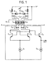
- a VCO comprises an integrated circuit shown below the dashed line A-A, and an external resonator shown above the dashed line A-A.
- the integrated circuit may of course contain many components (not shown) forming circuits which are not part of this embodiment of the invention and which will not be described.
- capacitors C P are parasitic capacitances and inductors L P are parasitic inductances, in this case the inductances of the bond wires connecting the integrated circuit to the external resonator.
- a first transistor T 1 has its collector coupled to Port 1 of the integrated circuit via a filter comprising a capacitor C F and an inductor L F and whose resonant frequency is within, preferably at the centre of, the frequency range of the VCO.
- a second transistor T 2 has its collector coupled to Port 2 of the integrated circuit, and its emitter coupled to the emitter of T 1 , both emitters being fed by a current source I 1 .
- the collector of T 1 is coupled via a capacitive divider, comprising capacitors C 1 , and C 2 , to the base of T 2 .
- the base of T 1 is decoupled by a capacitor C 3 .
- a capacitor C S couples the base of T 2 to Port 1, capacitor C S forming a series resonant circuit with the external resonator.
- Port 2 is decoupled by a capacitor C 4 .
- the collector of T 1 is also coupled to the base of a buffer transistor T 3 whose emitter provides the output of the VCO and is fed via a current source I 2 .
- the external resonator is connected to Ports 1 and 2 and comprises a variable capacitance diode D 1 , an inductor L 1 , e.g. a microstrip, and the various parasitic elements C P and L P .
- a variable capacitance diode D 1 e.g. a diode
- L 1 e.g. a microstrip
- C P and L P various parasitic elements
- the filter comprising capacitor C F and inductor L F causes the circuit to exhibit a negative impedance across ports 1 and 2.
- the circuit has been shown to be tunable over the intended frequency range and does not exhibit unwanted frequency hopping or mode switching.
Landscapes
- Engineering & Computer Science (AREA)
- Power Engineering (AREA)
- Inductance-Capacitance Distribution Constants And Capacitance-Resistance Oscillators (AREA)
- Vehicle Body Suspensions (AREA)
Priority Applications (4)
| Application Number | Priority Date | Filing Date | Title |
|---|---|---|---|
| EP98302510A EP0948127B1 (fr) | 1998-03-31 | 1998-03-31 | Améliorations de ou en relation avec des circuits intégrés pour oscillateurs commandés en tension |
| DE69801307T DE69801307T2 (de) | 1998-03-31 | 1998-03-31 | Verbesserungen an oder hinsichtlich integrierter Schaltungen für spannungsgesteuerte Oszillatoren |
| US09/277,488 US6140884A (en) | 1998-03-31 | 1999-03-26 | Integrated circuits for voltage controlled oscillators |
| JP09038599A JP3315092B2 (ja) | 1998-03-31 | 1999-03-31 | 電圧制御発振器のための集積回路に関する改良 |
Applications Claiming Priority (1)
| Application Number | Priority Date | Filing Date | Title |
|---|---|---|---|
| EP98302510A EP0948127B1 (fr) | 1998-03-31 | 1998-03-31 | Améliorations de ou en relation avec des circuits intégrés pour oscillateurs commandés en tension |
Publications (2)
| Publication Number | Publication Date |
|---|---|
| EP0948127A1 true EP0948127A1 (fr) | 1999-10-06 |
| EP0948127B1 EP0948127B1 (fr) | 2001-08-08 |
Family
ID=8234751
Family Applications (1)
| Application Number | Title | Priority Date | Filing Date |
|---|---|---|---|
| EP98302510A Expired - Lifetime EP0948127B1 (fr) | 1998-03-31 | 1998-03-31 | Améliorations de ou en relation avec des circuits intégrés pour oscillateurs commandés en tension |
Country Status (4)
| Country | Link |
|---|---|
| US (1) | US6140884A (fr) |
| EP (1) | EP0948127B1 (fr) |
| JP (1) | JP3315092B2 (fr) |
| DE (1) | DE69801307T2 (fr) |
Cited By (3)
| Publication number | Priority date | Publication date | Assignee | Title |
|---|---|---|---|---|
| US6474792B2 (en) | 2000-07-31 | 2002-11-05 | Canon Kabushiki Kaisha | Liquid discharge head, method for manufacturing liquid discharge head, head cartridge on which liquid discharge head is mounted, and liquid discharge apparatus |
| KR100423502B1 (ko) * | 2001-11-20 | 2004-03-18 | 삼성전자주식회사 | 엘씨공진기와 차동증폭기를 이용한 전압제어발진기 |
| EP1841057A1 (fr) * | 2006-03-27 | 2007-10-03 | ELMOS Semiconductor AG | Oscillateur harmonique efficace en puissance utilisant des dispositifs complémentaires et une seule broche |
Families Citing this family (8)
| Publication number | Priority date | Publication date | Assignee | Title |
|---|---|---|---|---|
| JP2003110358A (ja) * | 2001-09-27 | 2003-04-11 | Matsushita Electric Ind Co Ltd | 発振器 |
| WO2004045090A2 (fr) * | 2002-11-13 | 2004-05-27 | Vectron International | Module d'oscillateur comprenant un resonateur a tronçon ferme |
| US7158767B2 (en) * | 2003-10-24 | 2007-01-02 | Cts Corporation | Tuneable frequency translator |
| US7327035B2 (en) * | 2004-09-08 | 2008-02-05 | Texas Instruments Incorporated | System and method for providing a low frequency filter pole |
| US7230504B1 (en) | 2005-08-31 | 2007-06-12 | Silicon Laboratories, Inc. | Controlled oscillator |
| JP4763622B2 (ja) * | 2007-01-19 | 2011-08-31 | 株式会社日立製作所 | 電圧制御発振回路およびそれを用いた通信機器 |
| GB2449063A (en) * | 2007-04-27 | 2008-11-12 | Cambridge Semiconductor Ltd | A saturation control loop for a BJT or IGBT in a switching power supply |
| US8275336B2 (en) * | 2010-06-23 | 2012-09-25 | Richwave Technology Corp. | Apparatus and method for digitally controlling capacitance |
Citations (5)
| Publication number | Priority date | Publication date | Assignee | Title |
|---|---|---|---|---|
| GB2228154A (en) * | 1989-02-09 | 1990-08-15 | Plessey Co Plc | On-chip integrated oscillator circuits |
| US5140286A (en) * | 1991-08-02 | 1992-08-18 | Motorola, Inc. | Oscillator with bias and buffer circuits formed in a die mounted with distributed elements on ceramic substrate |
| EP0642215A1 (fr) * | 1993-09-06 | 1995-03-08 | Koninklijke Philips Electronics N.V. | Oscillateur |
| EP0660504A1 (fr) * | 1993-12-20 | 1995-06-28 | Sony Corporation | Circuit oscillateur |
| EP0785616A1 (fr) * | 1996-01-22 | 1997-07-23 | Telefonaktiebolaget Lm Ericsson | Dispositif équilibré intégré à semi-conducteur, fonctionnant avec un circuit résonnant en parallèle |
Family Cites Families (1)
| Publication number | Priority date | Publication date | Assignee | Title |
|---|---|---|---|---|
| DE19611610A1 (de) * | 1996-03-23 | 1997-09-25 | Philips Patentverwaltung | Oszillaotr |
-
1998
- 1998-03-31 DE DE69801307T patent/DE69801307T2/de not_active Expired - Fee Related
- 1998-03-31 EP EP98302510A patent/EP0948127B1/fr not_active Expired - Lifetime
-
1999
- 1999-03-26 US US09/277,488 patent/US6140884A/en not_active Expired - Lifetime
- 1999-03-31 JP JP09038599A patent/JP3315092B2/ja not_active Expired - Fee Related
Patent Citations (5)
| Publication number | Priority date | Publication date | Assignee | Title |
|---|---|---|---|---|
| GB2228154A (en) * | 1989-02-09 | 1990-08-15 | Plessey Co Plc | On-chip integrated oscillator circuits |
| US5140286A (en) * | 1991-08-02 | 1992-08-18 | Motorola, Inc. | Oscillator with bias and buffer circuits formed in a die mounted with distributed elements on ceramic substrate |
| EP0642215A1 (fr) * | 1993-09-06 | 1995-03-08 | Koninklijke Philips Electronics N.V. | Oscillateur |
| EP0660504A1 (fr) * | 1993-12-20 | 1995-06-28 | Sony Corporation | Circuit oscillateur |
| EP0785616A1 (fr) * | 1996-01-22 | 1997-07-23 | Telefonaktiebolaget Lm Ericsson | Dispositif équilibré intégré à semi-conducteur, fonctionnant avec un circuit résonnant en parallèle |
Cited By (3)
| Publication number | Priority date | Publication date | Assignee | Title |
|---|---|---|---|---|
| US6474792B2 (en) | 2000-07-31 | 2002-11-05 | Canon Kabushiki Kaisha | Liquid discharge head, method for manufacturing liquid discharge head, head cartridge on which liquid discharge head is mounted, and liquid discharge apparatus |
| KR100423502B1 (ko) * | 2001-11-20 | 2004-03-18 | 삼성전자주식회사 | 엘씨공진기와 차동증폭기를 이용한 전압제어발진기 |
| EP1841057A1 (fr) * | 2006-03-27 | 2007-10-03 | ELMOS Semiconductor AG | Oscillateur harmonique efficace en puissance utilisant des dispositifs complémentaires et une seule broche |
Also Published As
| Publication number | Publication date |
|---|---|
| JPH11346115A (ja) | 1999-12-14 |
| DE69801307T2 (de) | 2002-04-25 |
| DE69801307D1 (de) | 2001-09-13 |
| JP3315092B2 (ja) | 2002-08-19 |
| EP0948127B1 (fr) | 2001-08-08 |
| US6140884A (en) | 2000-10-31 |
Similar Documents
| Publication | Publication Date | Title |
|---|---|---|
| US7239209B2 (en) | Serially RC coupled quadrature oscillator | |
| EP0085241B1 (fr) | Oscillateur à configuration commutable | |
| US6140884A (en) | Integrated circuits for voltage controlled oscillators | |
| US6169461B1 (en) | High-frequency oscillating circuit | |
| US6806785B2 (en) | Oscillator circuit using bonding wires for inductors and having a resonance transformation circuit | |
| US6927643B2 (en) | Oscillator topology for very low phase noise operation | |
| US4754236A (en) | Frequency-doubling voltage-controlled oscillator | |
| US5025229A (en) | Voltage-controlled oscillator using a surface elastic wave resonator | |
| US7362193B2 (en) | Oscillator and an integrated circuit | |
| Kalia et al. | An ultra-low close-in phase noise series-resonance BAW oscillator in a 130-nm BiCMOS process | |
| JPH0746038A (ja) | 電圧制御周波数発振器 | |
| US5341111A (en) | Microwave oscillator circuit | |
| US6492879B2 (en) | Voltage-controlled oscillator | |
| JP2001060826A (ja) | 2バンド発振装置 | |
| EP1117177B1 (fr) | Oscillateur commandé en tension | |
| JP4657406B2 (ja) | 電圧制御発振器 | |
| JP4677696B2 (ja) | 平衡型発振回路およびそれを用いた電子装置 | |
| JP2918281B2 (ja) | 高周波発振回路 | |
| JP4365575B2 (ja) | テレビジョンチューナの発振回路 | |
| KR100538614B1 (ko) | 전압 제어 발진기 | |
| JP2002084136A (ja) | 発振回路 | |
| KR20020092241A (ko) | 전압 제어 발진기 및 그것을 사용한 전자장치 | |
| JPH104315A (ja) | 高周波発振回路 | |
| JP2001111342A (ja) | 2バンド発振器 | |
| EP1081846B1 (fr) | Oscillateur commandé en tension |
Legal Events
| Date | Code | Title | Description |
|---|---|---|---|
| PUAI | Public reference made under article 153(3) epc to a published international application that has entered the european phase |
Free format text: ORIGINAL CODE: 0009012 |
|
| AK | Designated contracting states |
Kind code of ref document: A1 Designated state(s): DE FI FR GB SE |
|
| AX | Request for extension of the european patent |
Free format text: AL;LT;LV;MK;RO;SI |
|
| 17P | Request for examination filed |
Effective date: 20000323 |
|
| AKX | Designation fees paid |
Free format text: DE FI FR GB SE |
|
| GRAG | Despatch of communication of intention to grant |
Free format text: ORIGINAL CODE: EPIDOS AGRA |
|
| RBV | Designated contracting states (corrected) |
Designated state(s): DE FI FR GB SE |
|
| GRAG | Despatch of communication of intention to grant |
Free format text: ORIGINAL CODE: EPIDOS AGRA |
|
| GRAG | Despatch of communication of intention to grant |
Free format text: ORIGINAL CODE: EPIDOS AGRA |
|
| GRAH | Despatch of communication of intention to grant a patent |
Free format text: ORIGINAL CODE: EPIDOS IGRA |
|
| 17Q | First examination report despatched |
Effective date: 20000112 |
|
| GRAH | Despatch of communication of intention to grant a patent |
Free format text: ORIGINAL CODE: EPIDOS IGRA |
|
| GRAA | (expected) grant |
Free format text: ORIGINAL CODE: 0009210 |
|
| AK | Designated contracting states |
Kind code of ref document: B1 Designated state(s): DE FI FR GB SE |
|
| PG25 | Lapsed in a contracting state [announced via postgrant information from national office to epo] |
Ref country code: FI Free format text: LAPSE BECAUSE OF FAILURE TO SUBMIT A TRANSLATION OF THE DESCRIPTION OR TO PAY THE FEE WITHIN THE PRESCRIBED TIME-LIMIT Effective date: 20010808 |
|
| REF | Corresponds to: |
Ref document number: 69801307 Country of ref document: DE Date of ref document: 20010913 |
|
| PG25 | Lapsed in a contracting state [announced via postgrant information from national office to epo] |
Ref country code: SE Free format text: LAPSE BECAUSE OF FAILURE TO SUBMIT A TRANSLATION OF THE DESCRIPTION OR TO PAY THE FEE WITHIN THE PRESCRIBED TIME-LIMIT Effective date: 20011108 |
|
| ET | Fr: translation filed | ||
| REG | Reference to a national code |
Ref country code: GB Ref legal event code: IF02 |
|
| PGFP | Annual fee paid to national office [announced via postgrant information from national office to epo] |
Ref country code: DE Payment date: 20020328 Year of fee payment: 5 |
|
| PLBE | No opposition filed within time limit |
Free format text: ORIGINAL CODE: 0009261 |
|
| STAA | Information on the status of an ep patent application or granted ep patent |
Free format text: STATUS: NO OPPOSITION FILED WITHIN TIME LIMIT |
|
| 26N | No opposition filed | ||
| PG25 | Lapsed in a contracting state [announced via postgrant information from national office to epo] |
Ref country code: DE Free format text: LAPSE BECAUSE OF NON-PAYMENT OF DUE FEES Effective date: 20031001 |
|
| PGFP | Annual fee paid to national office [announced via postgrant information from national office to epo] |
Ref country code: FR Payment date: 20140311 Year of fee payment: 17 |
|
| PGFP | Annual fee paid to national office [announced via postgrant information from national office to epo] |
Ref country code: GB Payment date: 20140326 Year of fee payment: 17 |
|
| GBPC | Gb: european patent ceased through non-payment of renewal fee |
Effective date: 20150331 |
|
| REG | Reference to a national code |
Ref country code: FR Ref legal event code: ST Effective date: 20151130 |
|
| PG25 | Lapsed in a contracting state [announced via postgrant information from national office to epo] |
Ref country code: GB Free format text: LAPSE BECAUSE OF NON-PAYMENT OF DUE FEES Effective date: 20150331 |
|
| PG25 | Lapsed in a contracting state [announced via postgrant information from national office to epo] |
Ref country code: FR Free format text: LAPSE BECAUSE OF NON-PAYMENT OF DUE FEES Effective date: 20150331 |