EP0948128B1 - Annulation de décalage DC dans un récepteur à quadrature - Google Patents
Annulation de décalage DC dans un récepteur à quadrature Download PDFInfo
- Publication number
- EP0948128B1 EP0948128B1 EP98400807A EP98400807A EP0948128B1 EP 0948128 B1 EP0948128 B1 EP 0948128B1 EP 98400807 A EP98400807 A EP 98400807A EP 98400807 A EP98400807 A EP 98400807A EP 0948128 B1 EP0948128 B1 EP 0948128B1
- Authority
- EP
- European Patent Office
- Prior art keywords
- frequency
- signal
- offset value
- demodulation
- cut
- Prior art date
- Legal status (The legal status is an assumption and is not a legal conclusion. Google has not performed a legal analysis and makes no representation as to the accuracy of the status listed.)
- Expired - Lifetime
Links
- 238000000034 method Methods 0.000 claims description 14
- 238000001228 spectrum Methods 0.000 claims description 12
- 238000001914 filtration Methods 0.000 claims description 11
- 230000003068 static effect Effects 0.000 claims description 9
- 238000005259 measurement Methods 0.000 claims description 8
- 230000003595 spectral effect Effects 0.000 claims 2
- 230000001419 dependent effect Effects 0.000 claims 1
- 238000012544 monitoring process Methods 0.000 claims 1
- 238000012937 correction Methods 0.000 description 5
- 230000010355 oscillation Effects 0.000 description 3
- 238000013459 approach Methods 0.000 description 1
- 238000006243 chemical reaction Methods 0.000 description 1
- 238000010586 diagram Methods 0.000 description 1
- 238000002955 isolation Methods 0.000 description 1
Images


Classifications
-
- H—ELECTRICITY
- H03—ELECTRONIC CIRCUITRY
- H03D—DEMODULATION OR TRANSFERENCE OF MODULATION FROM ONE CARRIER TO ANOTHER
- H03D3/00—Demodulation of angle-, frequency- or phase- modulated oscillations
- H03D3/007—Demodulation of angle-, frequency- or phase- modulated oscillations by converting the oscillations into two quadrature related signals
- H03D3/008—Compensating DC offsets
-
- H—ELECTRICITY
- H03—ELECTRONIC CIRCUITRY
- H03D—DEMODULATION OR TRANSFERENCE OF MODULATION FROM ONE CARRIER TO ANOTHER
- H03D3/00—Demodulation of angle-, frequency- or phase- modulated oscillations
- H03D3/007—Demodulation of angle-, frequency- or phase- modulated oscillations by converting the oscillations into two quadrature related signals
- H03D3/009—Compensating quadrature phase or amplitude imbalances
-
- H—ELECTRICITY
- H04—ELECTRIC COMMUNICATION TECHNIQUE
- H04L—TRANSMISSION OF DIGITAL INFORMATION, e.g. TELEGRAPHIC COMMUNICATION
- H04L25/00—Baseband systems
- H04L25/02—Details ; arrangements for supplying electrical power along data transmission lines
- H04L25/06—DC level restoring means; Bias distortion correction ; Decision circuits providing symbol by symbol detection
- H04L25/061—DC level restoring means; Bias distortion correction ; Decision circuits providing symbol by symbol detection providing hard decisions only; arrangements for tracking or suppressing unwanted low frequency components, e.g. removal of DC offset
Definitions
- This invention relates to demodulation methods and particularly but not exclusively to methods for demodulating a Radio-Frequency (RF) signal in a portable communications device.
- RF Radio-Frequency
- Portable communications devices such as mobile telephones typically operate with a limited power supply in the form of a battery, and hence have a limited period of operation before the battery must be recharged or replaced.
- DRX mode Discontinuous Receiving Mode
- a problem with the receiver apparatus is that whilst receiving and demodulating a signal, Direct Current (DC) interference generated internally interferes with the signal, limiting dynamic range.
- DC Direct Current
- a known solution to this problem is to provide in the receiver apparatus, a DC adapt step, prior to demodulating the signal, which substantially cancels the DC interference.
- the receiver apparatus must be switched on during this DC adapt step, thereby causing an increased 'on' time of the receiver apparatus and hence resulting in a large power drain.
- This invention seeks to provide a demodulation method which mitigates the above mentioned disadvantages.
- the DCR 5 has an antenna 7, coupled via a receive filter 8 to an amplifier and mixer stage 10, and a low frequency stage 100.
- the amplifier and mixer stage 10 has a low noise amplifier with an input coupled to receive a filtered RF signal from the receive filter 8 and an output which is split into two paths.
- a first path is coupled via a first mixer 30 to a first signal amplifier 40.
- a second path is coupled via a second mixer 50 to a second signal amplifier 60.
- the first and second mixers 30 and 50 are also coupled to receive sine and cosine components respectively of an oscillating signal from a fractional-N type synthesised oscillator 70. In this way the first and second mixers 30 and 50 and the first and second signal amplifiers 40 and 60 respectively provide in-phase (I) and quadrature (Q) mixed signals which are demodulated components of the RF signal.
- First and second Digital-to-Analogue Converters (DACs) 35 and 55 provide static offset values for the first and second mixers 30 and 50 respectively, to be further described below.
- Further DACs 75 provide phase and mismatch correction functions for the fractional-N oscillator 70, via a CR/RC network 77.
- the CR/RC network is a quadrature network generator that generates cosine and sine components of the fractional-N oscillator 70.
- the first and second signal amplifiers 40 and 60 each have gain control inputs, for adjusting the gain thereof.
- the low frequency stage 100 also has two paths.
- a first path which starts from the I signal of the first signal amplifier 40 (the I path) comprises (in sequence) a first bandwidth adjustment filter 110, a first low-frequency amplifier 120, a first Analogue-to-Digital (A/D) converter 130 and a first baseband filter 140.
- the output of the first baseband filter 140 is a signal Id(t).
- the second path which starts from the Q signal of the second signal amplifier 60 (the Q path) comprises (in sequence) a second bandwidth adjustment filter 160, a second low-frequency amplifier 170, a second A/D converter 180 and a second baseband filter 190.
- the output of the second baseband filter 190 is a signal Qd(t).
- the first and second bandwidth adjustment filters 110 and 160 and the first and second baseband filters 140 and 190 each have filter control inputs, to control the filtering thereof.
- the first and second low-frequency amplifiers 120 and 170 each have gain control inputs to control the gain thereof.
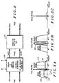
- FIG. 2 shows in greater detail a portion of the low frequency stage of FIG. 1, there is provided a gain/phase correction block 200 and a complex low-pass filter (LPF) 210.
- LPF complex low-pass filter
- the gain/phase correction block 200 is coupled to receive the Id(t) and Qd(t) signals and Gain adjustment (Ad) and Phase ( ⁇ ) control signals.
- the Ad and ⁇ control signals are factory set, and are intended to remove any phase or gain mismatches occurring between the I and Q paths as a result of analogue device variations. Any such mismatches could cause aliasing between channels of the receive spectrum.
- the Iout and Qout signals are then filtered by the complex LPF 210 to produce IDCest and QDCest signals representing the DC offset component of the Iout and Qout signals.
- the IDCest signal is then subtracted from the Iout signal, at a mux block 220.
- the QDCest signal is subtracted from the Qout signal, at a mux block 230. In this way the DC offset component of the Iout and Qout signals are substantially cancelled.
- a fast DC adapt step is achieved as follows.
- FIG. 3a there is shown a wanted spectrum 300 centred on the frequency f, and an adjacent channel spectrum 310. Gain and phase mismatches between the I and the Q paths result in aliased images of the wanted spectrum 300 and the adjacent channel spectrum 310, which appear as images 315 (image of the wanted spectrum 300) and 305 (image of the adjacent channel spectrum 310).
- a vector Vin(t) at the frequency F represents the DC offset derived from Id(t) and Qd(t).
- FIG. 3b shows a second vector Vout(t) (derived from Iout and Qout) representative of the gain and phase corrected DC offset.
- the gain and phase correction substantially removes the images 305 and 310 from the adjacent channel 310 and the wanted spectrum 300 respectively.
- a wideband envelope 350 of FIG. 3b represents the wideband filtering to be performed by the complex LPF 210.
- FIG. 3c shows the result of this filtering, in the form of a third vector VDC(t) (derived from IDCest and QDCest) which represents the DC offset.
- the DC offset value is based on a measurement shifted from the frequency f, and is therefore almost exclusively the result of internal interference. Also, it is possible during the fast DC adapt mode, to effectively switch off the amplifier and mixer stage 10, by switching off or reducing the gain of the LNA 20 in order to reduce the levels of wanted signals and adjacent channels versus the DC offsets. This RF isolation is of interest during the static DC offset value estimation.
- the fractional-N oscillator 70 is then set to oscillate at the frequency f, in order to provide the desired demodulated signal.
- the DC offset value given by IDCest and QDCest is then subtracted from the demodulated signal in order to provide a demodulated signal with a substantially reduced DC component.
- the blocks 200 and 210 then continue to provide further DC offset values, which are subtracted to further reduce the amount of DC offset present in the demodulated signal.
- the complex LPF 210 may be adjusted so as to have a different filter envelope to the wideband envelope 350 shown in FIG. 3b.
- the complex LPF 210 may, when filtering the demodulated signal, define a narrowband envelope.
- the first and second DACs 35 and 55 may be arranged to store the results of the fast DC adapt step described above, such that when the same wanted frequency is demodulated at a later time, the DACs 35 and 55 can provide appropriate static offset values for the first and second mixers 30 and 50 respectively, such that the fast DC adapt step need not be performed every time the wanted frequency is demodulated.
- a zero-IF (ZIF) RF receiver 400 of a portable communications device differs from the DCR receiver 100 of FIG. 1 in that the demodulation takes place in two stages, and there are two oscillators.
- a first stage 410 comprises a main synthesiser 420, which demodulates a received signal to an intermediate frequency (IF).
- the second stage 500 has a second oscillator 510, which is a low-order fractional-N synthesiser, coupled to provide oscillation signals to first and second mixers 505 and 515.
- the first and second mixers 505 and 515 split the IF signal from the first stage 410 into two paths, an I path and a Q path, similar to those of FIG. 1.
- the use of a similar approach to DCR in ZIF receiver 400 as in DCR is possible. However, a different type of cancellation is required for the ZIF receiver 400.
- the IF signal will always be at the same frequency (the intermediate frequency) and therefore the second oscillator 510 need only have two oscillation frequencies; the IF (for demodulation) and IF+ ⁇ (for the DC adapt step). During the fast DC adapt, the second oscillator 510 is shifted in frequency to IF+ ⁇ .
- the DC adapt is performed by a number of DC adapt blocks.
- DC adapt feedback blocks 520, 530, 550 and 560 are coupled to provide DC offset feedback cancellation for amplifiers 525, 535, 555 and 565.
- the DC adapt block 550 estimates the DC offsets of the first stage 410 through the use of a low pass filter (in a wideband configuration). This estimated DC offsets is compared to zero. The resulting error is integrated by an integrator and feedback to the input of the amplifier 555. This forms a DC adapt loop which will converge to zero DC output after a response time.
- the second oscillator 510 switches to the IF and the low pass filter of the DC adapt block 550 is set to a narrowband configuration to continue to estimate the DC offsets variation.
- the other DC adapt blocks 520, 530 and 560 operate in a similar way, and serve to increase the Dynamic range of each associated amplifier (525, 535 and 565) by substantially cancelling the associated DC offsets.
- Analogue DC adapt blocks 540 and 570 are also provided for the I and Q paths respectively, and these are required in the case that A/D converters 575 and 545 do not have enough dynamic range to accept amplified DC offsets present in the analogue signal.
- the complex LPF 210 could be replaced by one or more filters with different attributes, which result in substantially the same DC offset value.
Landscapes
- Engineering & Computer Science (AREA)
- Power Engineering (AREA)
- Computer Networks & Wireless Communication (AREA)
- Signal Processing (AREA)
- Noise Elimination (AREA)
- Superheterodyne Receivers (AREA)
Claims (9)
- Procédé de démodulation d'un signal de radiofréquence ou de fréquence intermédiaire possédant une première fréquence, le procédé comprenant les opérations suivantes :caractérisé en ce que la mesure de la valeur de décalage de courant continu comporte l'application dudit signal d'oscillateur localement produit audit moyen de démodulation avec une deuxième fréquence, la deuxième fréquence étant différente de la première fréquence, et un filtrage passe-bas ayant une fréquence de coupure de mesure, et en ce que la démodulation du signal de radiofréquence ou de fréquence intermédiaire comporte un filtrage ayant une fréquence de coupure de démodulation inférieure à ladite fréquence de coupure de mesure après l'application dudit signal d'oscillateur localement produit au moyen de démodulation avec la première fréquence.produire un signal d'oscillateur local ;mesurer la valeur du décalage de courant continu qui résulte de l'application dudit signal d'oscillateur localement produit à un moyen de démodulation, la valeur de décalage de courant continu étant associée avec des interférences internes ;appliquer au moyen de démodulation le signal d'oscillateur localement produit avec une première fréquence afin de démoduler le signal de radiofréquence ou de fréquence intermédiaire, si bien qu'il est produit un signal démodulé ;soustraire du signal démodulé la valeur de décalage de courant continu afin de produire un signal démodulé ayant une composante de courant continu sensiblement réduite ;contrôler le signal démodulé en vue de la recherche d'autres composantes de décalage de courant continu ; etsoustraire du signal démodulé les autres composantes de décalage de courant continu,
- Procédé selon la revendication 1, où la fréquence de coupure de démodulation et la fréquence de coupure de mesure sont produites par un moyen de filtrage passe-bas unique ayant des modes de fréquence de coupure supérieur et inférieur.
- Procédé selon la revendication 1 ou 2, où ledit filtrage effectué avec une fréquence de coupure de démodulation et avec une fréquence de coupure de mesure est effectué via l'utilisation de moyens de filtrage complexes.
- Procédé selon l'une quelconque des revendications précédentes, comprenant en outre les opérations suivantes :isoler le moyen de démodulation vis-à-vis du signal de radiofréquence pendant l'opération d'application du signal d'oscillateur localement produit au moyen de démodulation avec la deuxième fréquence ;mesurer une valeur de décalage de courant continu statique qui n'est sensiblement que les interférences internes du moyen de démodulation ;stocker la valeur de décalage de courant continu statique dans un moyen de stockage ;reconnecter le moyen de démodulation au signal de radiofréquence avant l'opération de mesure de la valeur de décalage de courant continu à partir de la deuxième fréquence.
- Procédé selon la revendication 4, comprenant en outre les opérations suivantes :retirer sensiblement la valeur de décalage de courant continu statique de la valeur de décalage de courant continu avant l'opération consistant à soustraire la valeur de décalage de courant continu du signal démodulé ; etsoustraire indépendamment le signal de décalage de courant continu statique du signal démodulé.
- Procédé selon la revendication 4 ou 5, comprenant en outre les opérations suivantes :mesurer une valeur de décalage de courant continu statique pour chaque configuration d'un certain nombre de configurations du moyen de démodulation ;stocker la valeur de décalage de courant continu statique dans un moyen de stockage ; etutiliser les valeurs stockées en fonction de la configuration choisie.
- Ensemble de démodulation servant à démoduler un signal de radiofréquence ou de fréquence intermédiaire ayant une première fréquence, l'ensemble comprenant :caractérisé en ce que, pour mesurer la valeur de décalage de courant continu, le moyen de démodulation répond audit signal d'oscillateur localement produit ayant une deuxième fréquence, la deuxième fréquence étant différente de la première fréquence, et en ce que le moyen de filtrage passe-bas ayant une fréquence de coupure de mesure qui est plus grande que ladite fréquence de coupure de démodulation mesure une valeur de décalage de courant continu sensiblement dépendante d'interférences internes.un oscillateur destiné à produire un signal d'oscillateur local ;un moyen de démodulation conçu pour mélanger le signal d'oscillateur localement produit ayant la première fréquence avec ledit signal de radiofréquence ou de fréquence intermédiaire ;ledit moyen de démodulation comportant un moyen de filtrage passe-bas servant à mesurer une valeur de décalage de courant continu, la valeur de décalage de courant continu étant associée à des interférences, ledit moyen de filtrage passe-bas ayant une fréquence de coupure de démodulation ; etun moyen de soustraction servant à soustraire la valeur de décalage de courant continu du signal démodulé afin de produire un signal démodulé ayant une composante de courant continu sensiblement réduite,
- Procédé ou ensemble selon l'une quelconque voulue des revendications précédentes, où la deuxième fréquence est choisie de façon à être à une fréquence associée avec un point de densité de puissance spectrale sensiblement minimale d'un spectre de puissance associé à la première fréquence.
- Procédé ou ensemble selon l'une quelconque voulue des revendications précédentes, où la deuxième fréquence est choisie de façon à être à une fréquence associée avec un point de densité de puissance spectrale sensiblement minimale d'un spectre de puissance associé avec l'intervalle de fréquence dudit moyen de démodulation.
Priority Applications (3)
| Application Number | Priority Date | Filing Date | Title |
|---|---|---|---|
| DE69827924T DE69827924T2 (de) | 1998-04-03 | 1998-04-03 | Unterdrückung von Gleichspannungsverschiebungen in einem Quadraturempfänger |
| EP98400807A EP0948128B1 (fr) | 1998-04-03 | 1998-04-03 | Annulation de décalage DC dans un récepteur à quadrature |
| US09/285,116 US6075409A (en) | 1998-04-03 | 1999-04-01 | Demodulation method and arrangement |
Applications Claiming Priority (2)
| Application Number | Priority Date | Filing Date | Title |
|---|---|---|---|
| EP98400807A EP0948128B1 (fr) | 1998-04-03 | 1998-04-03 | Annulation de décalage DC dans un récepteur à quadrature |
| US09/285,116 US6075409A (en) | 1998-04-03 | 1999-04-01 | Demodulation method and arrangement |
Publications (2)
| Publication Number | Publication Date |
|---|---|
| EP0948128A1 EP0948128A1 (fr) | 1999-10-06 |
| EP0948128B1 true EP0948128B1 (fr) | 2004-12-01 |
Family
ID=26151608
Family Applications (1)
| Application Number | Title | Priority Date | Filing Date |
|---|---|---|---|
| EP98400807A Expired - Lifetime EP0948128B1 (fr) | 1998-04-03 | 1998-04-03 | Annulation de décalage DC dans un récepteur à quadrature |
Country Status (2)
| Country | Link |
|---|---|
| US (1) | US6075409A (fr) |
| EP (1) | EP0948128B1 (fr) |
Families Citing this family (38)
| Publication number | Priority date | Publication date | Assignee | Title |
|---|---|---|---|---|
| US6148047A (en) * | 1998-05-06 | 2000-11-14 | Philips Electronics North America Corporation | DC offset compensation for zero if quadrature demodulator |
| DE69834407T2 (de) * | 1998-12-23 | 2007-04-19 | Asulab S.A. | Direktmischempfänger für FSK-modulierte Signale |
| GB2355900B (en) * | 1999-10-29 | 2004-03-17 | Ericsson Telefon Ab L M | Radio receiver |
| NO329890B1 (no) * | 1999-11-15 | 2011-01-17 | Hitachi Ltd | Mobilkommunikasjonsapparat |
| DE50109162D1 (de) | 2000-05-16 | 2006-05-04 | Infineon Technologies Ag | Schaltungsanordnung zur toleranzkorrektur in einem frequenzdemodulator |
| GR1003688B (el) * | 2000-07-14 | 2001-10-05 | Ιντρακομ Α.Ε. Ελληνικη Βιομηχανια Τηλεπικοινωνιων Και Συστηματ... | Μηχανισμος διορθωσης τασης εκτροπης και ενισχυτης ελεγχομενου κερδους σε δεκτες αμεσης μεταδοσης. |
| DE10044449A1 (de) * | 2000-09-08 | 2002-04-04 | Infineon Technologies Ag | Empfängerschaltung, insbesondere für den Mobilfunk |
| US6735422B1 (en) | 2000-10-02 | 2004-05-11 | Baldwin Keith R | Calibrated DC compensation system for a wireless communication device configured in a zero intermediate frequency architecture |
| US6560448B1 (en) * | 2000-10-02 | 2003-05-06 | Intersil Americas Inc. | DC compensation system for a wireless communication device configured in a zero intermediate frequency architecture |
| US7068987B2 (en) | 2000-10-02 | 2006-06-27 | Conexant, Inc. | Packet acquisition and channel tracking for a wireless communication device configured in a zero intermediate frequency architecture |
| ATE313166T1 (de) * | 2000-10-30 | 2005-12-15 | Texas Instruments Inc | Vorrichtung zum ausgleichen des dc-offsets eines quadratur-demodulators , und verfahren dazu |
| US6697611B1 (en) * | 2000-11-14 | 2004-02-24 | Intel Corporation | Method and apparatus for performing DC offset cancellation in a receiver |
| DE60107816T2 (de) | 2000-11-23 | 2005-12-01 | Koninklijke Philips Electronics N.V. | Korrekturschaltung für gleichspannungsoffset mit gleichspannungsregelungsschleife und gleichspannungsblockierungsschaltung |
| US6839551B1 (en) * | 2001-05-21 | 2005-01-04 | National Semiconductor Corporation | Radio frequency mixer and method of operation |
| DE10131676A1 (de) * | 2001-06-29 | 2003-01-16 | Infineon Technologies Ag | Empfängeranordnung mit Wechselstrom-Kopplung |
| US6670901B2 (en) * | 2001-07-31 | 2003-12-30 | Motorola, Inc. | Dynamic range on demand receiver and method of varying same |
| KR100403814B1 (ko) * | 2001-08-13 | 2003-10-30 | 삼성전자주식회사 | 멀티칩 모듈을 이용하여 디.씨 옵셋을 감소시킨 다이렉트컨버젼 수신기 |
| US7356326B2 (en) * | 2001-12-12 | 2008-04-08 | Samsung Electronics Co., Ltd. | Direct-conversion receiver for removing DC offset |
| JP3743374B2 (ja) * | 2002-02-04 | 2006-02-08 | 株式会社村田製作所 | フィルタモジュールの製造方法 |
| US6862439B2 (en) * | 2002-06-28 | 2005-03-01 | Nokia Corporation | Offset compensation in a direct-conversion receiver |
| US7110734B2 (en) * | 2002-09-05 | 2006-09-19 | Maxim Integrated Products Inc. | DC offset cancellation in a zero if receiver |
| KR20040049563A (ko) * | 2002-12-06 | 2004-06-12 | 한국전자통신연구원 | 무선 이동통신 시스템의 직접변환 수신 장치 및 그 방법 |
| US8150362B2 (en) * | 2003-04-03 | 2012-04-03 | Maxim Integrated Products, Inc. | Electronically tuned agile integrated bandpass filter |
| US7412222B2 (en) | 2003-05-20 | 2008-08-12 | Broadcom Corporation | Quadrature correction method for analog television reception using direct-conversion tuners |
| US7277688B2 (en) * | 2003-06-17 | 2007-10-02 | Broadcom Corporation | DC offset correction for very low intermediate frequency receiver |
| US7295250B2 (en) | 2003-07-31 | 2007-11-13 | Broadcom Corporation | Apparatus and method for restoring DC spectrum for analog television reception using direct conversion turners |
| EP1515429B1 (fr) * | 2003-08-25 | 2008-08-20 | Nokia Corporation | Récepteur à conversion directe et méthode de récéption |
| FI20031194A0 (fi) | 2003-08-25 | 2003-08-25 | Nokia Corp | Suoramuuntovastaanotin ja vastaanottomenetelmä |
| US7596195B2 (en) | 2004-03-31 | 2009-09-29 | Broadcom Corporation | Bandpass filter with reversible IQ polarity to enable a high side or low side injection receiver architecture |
| US7603098B2 (en) | 2004-03-31 | 2009-10-13 | Broadcom Corporation | Programmable IF frequency filter for enabling a compromise between DC offset rejection and image rejection |
| DE102004047424A1 (de) * | 2004-09-28 | 2006-04-06 | Micronas Gmbh | Schaltung und Verfahren zur Trägerrückgewinnung |
| DE102004048572A1 (de) * | 2004-10-04 | 2006-04-13 | Micronas Gmbh | Verfahren sowie Schaltungsanordnung zur Unterdrückung einer orthogonalen Störung |
| DE102004054893A1 (de) * | 2004-11-12 | 2006-05-24 | Micronas Gmbh | Verfahren und Schaltungsanordnung zur Kanalfilterung analog oder digital modulierter TV-Signale |
| US7583765B2 (en) * | 2005-04-26 | 2009-09-01 | Skyworks Solutions, Inc. | DC offset detection and cancellation in a receiver |
| US8036622B2 (en) * | 2005-09-28 | 2011-10-11 | Qualcomm, Incorporated | DC offset cancellation circuit for a receiver |
| US7830991B2 (en) * | 2005-10-03 | 2010-11-09 | Harris Corporation | Frequency selective automatic gain control with dual non-symmetric attack and release times and interference detection feature |
| US7622987B1 (en) | 2007-01-25 | 2009-11-24 | Pmc-Sierra, Inc. | Pattern-based DC offset correction |
| US10511462B2 (en) | 2016-01-06 | 2019-12-17 | Apple Inc. | DC offset cancelation for wireless communications |
Family Cites Families (11)
| Publication number | Priority date | Publication date | Assignee | Title |
|---|---|---|---|---|
| US3568078A (en) * | 1968-12-23 | 1971-03-02 | Radiation Inc | Fm demodulators with signal error removal |
| US3953805A (en) * | 1974-11-07 | 1976-04-27 | Texas Instruments Incorporated | DC component suppression in zero CF IF systems |
| US4105975A (en) * | 1977-02-01 | 1978-08-08 | Ncr Corporation | Offset correction circuit for phase detectors |
| NL190886C (nl) * | 1986-05-19 | 1994-10-03 | Nippon Telegraph & Telephone | Digitaal signaaldemodulatiesysteem. |
| US5212826A (en) * | 1990-12-20 | 1993-05-18 | Motorola, Inc. | Apparatus and method of dc offset correction for a receiver |
| US5157697A (en) * | 1991-03-21 | 1992-10-20 | Novatel Communications, Ltd. | Receiver employing correlation technique for canceling cross-talk between in-phase and quadrature channels prior to decoding |
| US5548244A (en) * | 1994-11-14 | 1996-08-20 | Hughes Aircraft Company | Method and apparatus for eliminating DC offset for digital I/Q demodulators |
| US5724653A (en) * | 1994-12-20 | 1998-03-03 | Lucent Technologies Inc. | Radio receiver with DC offset correction circuit |
| GB9617423D0 (en) * | 1995-10-11 | 1996-10-02 | Philips Electronics Nv | Receiver circuit |
| US5881376A (en) * | 1995-12-15 | 1999-03-09 | Telefonaktiebolaget Lm Ericsson | Digital calibration of a transceiver |
| WO1998010523A1 (fr) * | 1996-09-06 | 1998-03-12 | Philips Electronics N.V. | Recepteur a frequence intermediaire nulle |
-
1998
- 1998-04-03 EP EP98400807A patent/EP0948128B1/fr not_active Expired - Lifetime
-
1999
- 1999-04-01 US US09/285,116 patent/US6075409A/en not_active Expired - Lifetime
Also Published As
| Publication number | Publication date |
|---|---|
| US6075409A (en) | 2000-06-13 |
| EP0948128A1 (fr) | 1999-10-06 |
Similar Documents
| Publication | Publication Date | Title |
|---|---|---|
| US6075409A (en) | Demodulation method and arrangement | |
| US6978125B2 (en) | Methods and apparatus for tuning pre-selection filters in radio receivers | |
| EP1058396B1 (fr) | Procédé et circuit de réception à fréquence intermédiare très basse | |
| EP1320198B1 (fr) | Récepteur à conversion direct avec de moins de suppresion de décalage de composant continue | |
| KR100682773B1 (ko) | 무선 수신기용 디씨 오프셋 정정 방법 | |
| US6148047A (en) | DC offset compensation for zero if quadrature demodulator | |
| JP3178997B2 (ja) | 周波数変換回路およびこの周波数変換回路を備えた無線通信装置 | |
| US6757340B1 (en) | Radio receiver and method for preloading an average DC-offset into a channel filter | |
| KR20010040991A (ko) | 레이크 수신기를 위한 자동 주파수 제어 루프 다경로 결합기 | |
| JP2002135157A (ja) | マルチバンド携帯無線端末 | |
| FI112131B (fi) | Menetelmä ja piirijärjestely signaalin erojännitteen pienentämiseksi | |
| US6507627B1 (en) | Direct conversion receiving apparatus with DC component cut function | |
| EP1551099A1 (fr) | Récepteur radio à fréquence intermediaire basse | |
| JP3672189B2 (ja) | 無線信号受信装置及び復調処理回路 | |
| JP2003046403A (ja) | ダイレクトコンバージョン受信機 | |
| JP3486058B2 (ja) | Dcオフセット除去機能を備えた受信機 | |
| US8121575B2 (en) | Modulated IF receiver and method | |
| KR20050073586A (ko) | 무선 수신기 및 am 억제와 dc-오프셋 제거를 위한 방법 | |
| JP3132459B2 (ja) | ダイレクトコンバージョン受信機 | |
| JPH1093475A (ja) | 複合システム共用端末 | |
| US7505744B1 (en) | DC offset correction using multiple configurable feedback loops | |
| US7751303B2 (en) | Demodulation circuit for use in receiver using if directing sampling scheme | |
| Zamat et al. | Introducing software defined radio to 4G wireless: Necessity, advantage, and impediment | |
| KR100764522B1 (ko) | 복소 신호들을 곱하기 위한 곱셈기 | |
| JPH10313261A (ja) | 妨害波抑圧回路、妨害波抑圧方法及び無線受信機 |
Legal Events
| Date | Code | Title | Description |
|---|---|---|---|
| PUAI | Public reference made under article 153(3) epc to a published international application that has entered the european phase |
Free format text: ORIGINAL CODE: 0009012 |
|
| AK | Designated contracting states |
Kind code of ref document: A1 Designated state(s): DE FR GB |
|
| AX | Request for extension of the european patent |
Free format text: AL;LT;LV;MK;RO;SI |
|
| 17P | Request for examination filed |
Effective date: 20000406 |
|
| AKX | Designation fees paid |
Free format text: DE FR GB |
|
| 17Q | First examination report despatched |
Effective date: 20020502 |
|
| GRAP | Despatch of communication of intention to grant a patent |
Free format text: ORIGINAL CODE: EPIDOSNIGR1 |
|
| GRAS | Grant fee paid |
Free format text: ORIGINAL CODE: EPIDOSNIGR3 |
|
| GRAA | (expected) grant |
Free format text: ORIGINAL CODE: 0009210 |
|
| AK | Designated contracting states |
Kind code of ref document: B1 Designated state(s): DE FR GB |
|
| REG | Reference to a national code |
Ref country code: GB Ref legal event code: FG4D |
|
| REF | Corresponds to: |
Ref document number: 69827924 Country of ref document: DE Date of ref document: 20050105 Kind code of ref document: P |
|
| PLBE | No opposition filed within time limit |
Free format text: ORIGINAL CODE: 0009261 |
|
| STAA | Information on the status of an ep patent application or granted ep patent |
Free format text: STATUS: NO OPPOSITION FILED WITHIN TIME LIMIT |
|
| ET | Fr: translation filed | ||
| 26N | No opposition filed |
Effective date: 20050902 |
|
| REG | Reference to a national code |
Ref country code: GB Ref legal event code: 732E |
|
| REG | Reference to a national code |
Ref country code: FR Ref legal event code: TP |
|
| PGFP | Annual fee paid to national office [announced via postgrant information from national office to epo] |
Ref country code: GB Payment date: 20070313 Year of fee payment: 10 |
|
| PGFP | Annual fee paid to national office [announced via postgrant information from national office to epo] |
Ref country code: DE Payment date: 20070430 Year of fee payment: 10 |
|
| PGFP | Annual fee paid to national office [announced via postgrant information from national office to epo] |
Ref country code: FR Payment date: 20070404 Year of fee payment: 10 |
|
| GBPC | Gb: european patent ceased through non-payment of renewal fee |
Effective date: 20080403 |
|
| PG25 | Lapsed in a contracting state [announced via postgrant information from national office to epo] |
Ref country code: DE Free format text: LAPSE BECAUSE OF NON-PAYMENT OF DUE FEES Effective date: 20081101 |
|
| REG | Reference to a national code |
Ref country code: FR Ref legal event code: ST Effective date: 20081231 |
|
| PG25 | Lapsed in a contracting state [announced via postgrant information from national office to epo] |
Ref country code: FR Free format text: LAPSE BECAUSE OF NON-PAYMENT OF DUE FEES Effective date: 20080430 |
|
| PG25 | Lapsed in a contracting state [announced via postgrant information from national office to epo] |
Ref country code: GB Free format text: LAPSE BECAUSE OF NON-PAYMENT OF DUE FEES Effective date: 20080403 |