EP0948155A2 - Amplitudenmultiplexierung von digitalen Signalen - Google Patents
Amplitudenmultiplexierung von digitalen Signalen Download PDFInfo
- Publication number
- EP0948155A2 EP0948155A2 EP99105208A EP99105208A EP0948155A2 EP 0948155 A2 EP0948155 A2 EP 0948155A2 EP 99105208 A EP99105208 A EP 99105208A EP 99105208 A EP99105208 A EP 99105208A EP 0948155 A2 EP0948155 A2 EP 0948155A2
- Authority
- EP
- European Patent Office
- Prior art keywords
- signal
- digital
- transmission
- level
- data
- Prior art date
- Legal status (The legal status is an assumption and is not a legal conclusion. Google has not performed a legal analysis and makes no representation as to the accuracy of the status listed.)
- Granted
Links
- 230000005540 biological transmission Effects 0.000 claims abstract description 100
- 238000000034 method Methods 0.000 claims abstract description 24
- 238000001914 filtration Methods 0.000 claims description 6
- 230000003287 optical effect Effects 0.000 claims description 6
- 230000001360 synchronised effect Effects 0.000 claims description 6
- 238000010586 diagram Methods 0.000 description 11
- 230000008054 signal transmission Effects 0.000 description 5
- 230000000630 rising effect Effects 0.000 description 4
- 238000012217 deletion Methods 0.000 description 2
- 230000037430 deletion Effects 0.000 description 2
- 238000011161 development Methods 0.000 description 2
- 230000018109 developmental process Effects 0.000 description 2
- 239000008186 active pharmaceutical agent Substances 0.000 description 1
- 230000002349 favourable effect Effects 0.000 description 1
- 238000004519 manufacturing process Methods 0.000 description 1
- 238000007781 pre-processing Methods 0.000 description 1
- 239000004065 semiconductor Substances 0.000 description 1
Images




Classifications
-
- H—ELECTRICITY
- H03—ELECTRONIC CIRCUITRY
- H03M—CODING; DECODING; CODE CONVERSION IN GENERAL
- H03M9/00—Parallel/series conversion or vice versa
-
- G—PHYSICS
- G11—INFORMATION STORAGE
- G11B—INFORMATION STORAGE BASED ON RELATIVE MOVEMENT BETWEEN RECORD CARRIER AND TRANSDUCER
- G11B7/00—Recording or reproducing by optical means, e.g. recording using a thermal beam of optical radiation by modifying optical properties or the physical structure, reproducing using an optical beam at lower power by sensing optical properties; Record carriers therefor
- G11B7/004—Recording, reproducing or erasing methods; Read, write or erase circuits therefor
- G11B7/006—Overwriting
- G11B7/0062—Overwriting strategies, e.g. recording pulse sequences with erasing level used for phase-change media
-
- H—ELECTRICITY
- H04—ELECTRIC COMMUNICATION TECHNIQUE
- H04L—TRANSMISSION OF DIGITAL INFORMATION, e.g. TELEGRAPHIC COMMUNICATION
- H04L5/00—Arrangements affording multiple use of the transmission path
- H04L5/02—Channels characterised by the type of signal
- H04L5/04—Channels characterised by the type of signal the signals being represented by different amplitudes or polarities, e.g. quadriplex
Definitions
- the invention relates to a method according to the preamble of the claim 1.
- the invention has for its object a method according to the preamble of claim 1 specify that with simple circuit means is feasible and that the transmission of digital signals via allows a small number of signal lines.
- the idea essential to the invention lies in the fact that it is to be transmitted digital transmission signals a multi-level signal with several equidistantly spaced generate a logical signal level via a signal line is transmitted from the transmitting unit to the receiving unit and there by means of amplitude filtering in the digital transmission signals digital received signals is broken down.
- the multi-level signal in the receiving unit with between the possible logical signal levels compared comparison thresholds, the comparison result being the digital received signals are formed. Because of the equidistantly spaced Signal level of the multi-level signal is an optimal use of the dynamic range and a favorable noise behavior guaranteed.
- bit information e.g., bit information
- data enable signal e.g., bit information
- logical links ensure that before the summation of the digital transmission signals partial areas of the data signal by the clock signal and possibly partial areas of the data release signal by the clock signal or Parts of the clock signal are hidden by the data enable signal become. This means that, with the exception of one of the transmission signals, each of the remaining transmit signals only at an active signal level one of the other transmission signals can assume its active signal level, each of the transmit signals being either a high level or a low level can have as an active signal level.
- one of the transmission signals is a low active signal, d. H. has a low level as the active signal level, then this transmission signal for forming the multi-level signal in the Transmitter unit with a negative sign added to the other transmission signals.
- the digital received signals, the clock signal, the data signal and possibly the data enable signal regenerates. To disturbances resulting from the clock signal to avoid, the latter is advantageously only during the data transmission provided.
- a preferred application of the method is the signal transmission via flexible lines between a transmitting unit and a receiving unit that is movable relative to the transmitting unit.
- One such application is, for example, the control of a laser diode driver which can be moved in a drive for rewritable optical storage disks.
- the data signal, the clock signal and the data enable signal for setting various parameters of the laser diode driver, e.g. B. the laser power for different operating modes, and a write signal, a read signal and an erase signal for controlling the laser power in the different operating modes, in particular in the operating modes Write", Read and Erase "is used on the reception side.
- the reception signals corresponding to the write, read and erase signals are formed, the reception signals are each weighted with a weighting factor and, after weighting, summed to form a control signal for a laser diode.
- the method thus enables both the transmission of amplitude information, ie the laser power for the various operating modes, as well as the transmission of any time information contained in the pulse widths of the write, read or erase signal.
- a multi-level signal from the write signal, the Erase signal and the read signal are formed or there are two multi-level signals from the write signal, the read signal, the erase signal, the clock signal, the data signal and the data enable signal formed, which then over two signal lines from a control unit, d. H. from the transmitter unit, to the laser diode driver, d. H. to the receiving unit.
- the data signal is preferably simultaneous with the data release signal and the clock signal and the write signal simultaneously with the the delete signal, however, each in different time windows, i. H. in the Time division multiplex over which a signal line and a write enable signal, the marked a time window in which the write and delete signals are transmitted be, as well as the read signal as another multi-level signal on the other Transfer the signal line to the receiving unit.
- the digital transmission signals s 11 , s 12 ... s 1n are summed in the transmission unit 1 to form the multi-level signal m, which is transmitted via the signal line 2 from the transmission unit 1 to the reception unit 3.
- the signal line 2 can be designed symmetrically, ie have two wires for differential signal transmission, or can be designed asymmetrically, ie have a wire as a feed line and a wire as a reference line for a reference potential, for example for a ground or supply potential. In the present example, it is flexible; Furthermore, the transmitting unit 1 and the receiving unit 3 are integrated on different semiconductor chips and can be moved relative to one another.
- 3n is provided in the receiving unit 3 for amplitude filtering for each of the digital transmission signals s 11 , s 12 ... s 1n , which compares the multi-level signal m with one between two adjacent logical signal levels of the multi-level signal m lying signal threshold V 1 or V 2 or ... V n and, as a comparison result, the digital reception signal s 31 or s 32 or corresponding to the respective digital transmission signal s 11 or s 12 or ... s 1n . .. s 3n delivers.
- the distances between the logical signal levels of the multi-level signal m are essentially the same, so that an optimal utilization of the dynamic range is ensured.
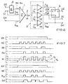
- FIG. 2 a clock signal SC and a serial data signal SD, which is synchronous with this and contains the data as information, are linked by means of an AND gate 4 to an intermediate signal z 4 , which is transmitted to the transmission unit 1 as the first digital transmission signal s 11 is supplied.
- the clock signal SC is supplied to the transmission unit 1 as a second digital transmission signal s 12 .
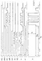
- FIG. 3 shows that by ANDing the data signal SD with the clock signal SC, the areas of the data signal SD which have a high level H are faded out by the clock signal SC in half and that the bit information of the data signal SD is obtained in the intermediate signal z 4 thus generated remains so that the first digital transmission signal s 11 can only assume a high level when the second digital transmission signal s 12 is high.
- the intermediate signal z 4 and the clock signal SC - the latter is fed to the transmission unit 1 as a second digital transmission signal s 12 - are summed in the transmission unit 1 to form the multi-level signal m, which has three logic signal levels with the levels L, H 1 and H 2 .
- the multi-level signal m is transmitted via the signal line 2 to the receiving unit 3, where it is compared in the first comparator 31 with the first signal threshold V 1 above the average logic signal level H 1 and in the second comparator 32 with the second signal threshold below the average logic signal level H 1 V 2 compared.
- the first comparator 31 supplies the first digital reception signal s 31 corresponding to the first digital transmission signal s 11 and the second comparator 32 the regenerated clock signal SC ', ie the second digital reception signal s 32 corresponding to the second digital transmission signal s 12 and the same as the clock signal SC .
- the data signal SD is regenerated on the receiving side with the D flip-flop 6, the D input of which is constantly at a low level.
- the flip-flop 6 is set with a high level of the first digital reception signal s 31 and a clock period later with the rising edge of the second digital reception signal s 32 is reset in an edge-controlled manner, so that the regenerated data signal SD 'is emitted at its output Q.
- the circuit arrangement from FIG. 2 can be supplemented with a further AND gate 5, a further flip-flop 7 and a third comparator 33 to form the circuit arrangement shown in FIG.
- a data enable signal EN is used to form the multi-level signal m, the validity of the data signal SD being marked and the data transmission being activated with the data enable signal EN.
- the clock signal SC is continuously transmitted.
- the data enable signal EN and the clock signal SC are combined to form a further intermediate signal z 5 , which is supplied to the transmission unit 1 as a third digital transmission signal s 13 .
- the third digital transmission signal s 13 can therefore only assume a high level when the second digital transmission signal s 12 is high.
- the multi-level signal m formed by summation of the three digital transmission signals s 11 , s 12 , s 13 has four logic signal levels, namely the levels L, H 1 , H 2 and H 3 .
- the multi-level signal m is fed to the three comparators 31, 32, 33.
- the first comparator 31 compares the multi-level signal m with the comparison threshold V 1 lying between the two highest logic signal levels H 3 and H 2 of the multi-level signal m and delivers as a comparison result the first digital received signal corresponding to the first digital transmit signal s 11 and containing the bit information of the data signal SD s 31 ;
- the second comparator 32 compares the multi-level signal m with the comparison threshold V 2 lying between the two lowest logic signal levels L and H 2 of the multi-level signal m and delivers as comparison result SC 'the second digital reception signal s corresponding to the second digital transmission signal s 12 and the same as the clock signal SC 32 ;
- the third comparator 33 finally compares the multi-level signal m with the comparison threshold V 3 lying between the two central logic signal levels H 1 and H 2 of the multi-level signal m and supplies as a comparison result the third digital reception signal s 33 corresponding to the third digital transmission signal s 13.
- the data signal SD is regenerated similarly to the circuit arrangement from FIG. 2 with the flip-flop 6, which is set with the high level H of the first digital received signal s 31 , ie is set level-controlled and one clock period later with the rising edge of the second digital received signal s 32 edge reset is reset.
- the data enable signal EN is regenerated with the further flip-flop 7, which is set at the high level H of the third digital reception signal s 33 and is reset edge-controlled a clock period later with the rising edge of the second digital reception signal s 32 .
- the regenerated data signal DS 'and the regenerated data enable signal EN' can be further processed with D-flip-flops, not shown in the figure, which are clocked in phase opposition to the flip-flops 6 and 7, in order to produce signal peaks which may arise due to differences in transit time , to suppress.
- FIG. 6 shows a further development of the circuit arrangement from FIG. 2, which differs from the circuit arrangement according to FIG. 2 in that the transmission unit 1 in addition to the first digital transmission signal s 11 which is the same as the intermediate signal z 4 and the second digital transmission signal s 12 which is the same as the clock signal SC a third digital transmission signal s 13 is supplied, which is equal to the data release signal EN with which the validity of the data signal SD is marked, and that the data release signal EN is regenerated in the receiving unit 3 with a third comparator 33.
- the clock signal SC is only present during the data transmission. Interference resulting from the clock signal SC is therefore largely avoided.
- the data signal SD and the clock signal SC are only at a high level H of the data release signal EN at a high level.
- the data signal SD and the clock signal SC are each AND-linked to the data enable signal.
- the AND gate 4 for example, the data signal SD and the clock signal SC to the intermediate signal 4, it is ensured that the z the intermediate signal 4 equal first digital transmission signal s of the clock signal SC assume a high level only in a high level 11 can.
- the digital transmission signals s 11 , s 12 , s 13 are summed to form the multi-level signal m with the four logic signal levels L, H 1 , H 2 and H 3 .
- the multi-level signal m is fed to the three comparators 31, 32, 33.
- the first comparator 31 compares the multi-level signal m with the comparison threshold V 1 lying between the two highest logic signal levels H 3 and H 2 of the multi-level signal m and delivers as a comparison result the first digital received signal corresponding to the first digital transmit signal s 11 and containing the bit information of the data signal SD s 31 ;
- the second comparator 32 compares the multi-level signal m with the comparison threshold V 2 lying between the two central logic signal levels H 1 and H 2 of the multi-level signal m and delivers as comparison result SC 'the second digital reception signal corresponding to the second digital transmission signal s 12 and the clock signal SC s 32 ;
- the third comparator 33 finally compares the multi-level signal m with the comparison threshold V 3 lying between the two lowest logic signal levels L and H 1 of the multi-level signal m and delivers as comparison result EN 'the third digital transmission signal s 13 corresponding to the third digital transmission signal EN and the same as the data enable signal EN Receive signal s 33 .
- the data signal SD is regenerated in the same way as in the circuit arrangement from FIG. 2 with the flip-flop 6, which is set at the high level H of the first digital received signal s 31 and one clock period later with the rising edge of the second digital received signal s 32 edge reset is reset.
- the flip-flop 6 is additionally reset with the low level L of the third digital received signal s 33 independently of the clock.
- the circuit arrangement according to FIG. 8 is used in a drive for storage media, in particular for rewritable optical storage disks, for transmitting a write signal WR, an erase signal ER and a read signal RD from the transmitter unit 1 via the signal line 2 to the receiver unit 3.
- the write signal WR which is supplied to the transmission unit 1 as the first digital transmission signal s 11
- the writing of data-representing markings on the storage medium is controlled
- the erase signal ER which is supplied to the transmission unit 1 as the second digital transmission signal s 12
- the deletion of the markings is controlled by the storage medium and the reading of the markings is controlled by the storage medium using the read signal RD, which is supplied to the transmission unit 1 as the third digital transmission signal s 13 .
- Erasing is understood here to mean the writing of a marking corresponding to a predetermined bit value, for example bit value 0.
- the transmission unit 1 is part of a control unit controlling the drive and the reception unit 3 is part of a laser diode driver, not shown in the figure, which is mounted on a write / erase disk that can be moved over the storage disk.
- / Read head is attached and with which the optical power of a laser diode is controlled according to the desired action (writing, erasing or reading). According to FIG.
- the write signal WR has a high level H only when the erase signal ER is active, ie when the erase signal ER is at a high level H. Furthermore, the erase signal ER has a high level only when the read signal RD is at a high level.
- the multi-level signal m is transmitted via the signal line 2 to the receiving unit 3, where it is broken down into the digital received signals s 31 , s 32 , s 33 by means of amplitude filtering with the comparators 31, 32, 33.
- the first comparator 31 compares the multi-level signal m with the comparison threshold V 1 lying between the two highest logic signal levels H 3 and H 2 of the multi-level signal m and delivers the first digital transmission signal s 11 corresponding to the first digital transmission signal s 11 and the same as the write signal WR Received signal S 31 ;
- the second comparator 32 compares the multi-level signal m with the comparison threshold V 2 lying between the two middle logic signal levels H 1 and H 2 of the multi-level signal m and delivers as a comparison result ER 'the second digital reception signal corresponding to the second digital transmission signal s 12 and the same as the deletion signal ER s 32 ;
- the third comparator 33 finally compares the multi-level signal m with the comparison threshold V 3 lying between the two lowest logic signal levels L and H 1 of the multi-level signal m and delivers as comparison result RD 'the third digital transmission signal s 13 corresponding to the third reading signal RD and the same Receive signal s 33 .
- the circuit arrangement from FIG. 10 shows an embodiment of the circuit arrangement from Figure 8, in which the write signal WR, the erase signal ER, a write enable signal WEN, which marks a time window in which the Write signal WR and erase signal ER are transmitted, and the read signal RD and the clock signal SC, the serial data signal SD, the bit information are contained in bit cells synchronous with the clock signal SC, and that Data release signal EN, with which the validity of the data signal SD is marked is sent to the transmission unit 1 as digital transmission signals, and in which the transmission unit 1 from these transmission signals two multi-level signals m, m 'generated, each via one of the signal lines 2, 2' to the receiving unit 3 are transmitted.
- the receiving unit 3 then trains the two multi-level signals m, m ', the digital received signals WR', ER ', WEN ', SD', SC ', EN', RD ', the digital transmit signals WR, ER, WEN, SD, SC, EN, RD correspond.
- the read signal RD has a high level during the entire signal transmission and the write enable signal WEN during the transmission of the write signal WR and the erase signal ER.
- the clock signal SC, data signal SD and the data release signal EN are combined in a first time window and in a subsequent time window the write signal WR and erase signal ER are combined to form the multi-level signal m, so that the latter, which is transmitted via the signal line 2 to the reception unit 3, has four logical signal levels L, H 1 , H 2 and H 3 .
- the further multi-level signal m ' which is generated by summation of the read signal RD and the write enable signal WEN and is transmitted via the further signal line 2' to the receiving unit 3, has three logical signal levels L, H 1 and H 2 .
- the signal line 2 is designed symmetrically, the other signal line 2 ', on the other hand, is single-pole due to the uncritical time requirements for the further multi-level signal m' or the read signal RD and write enable signal WEN.
- the receiving unit 3 is based on the by amplitude filtering the further multi-level signal m 'regenerated write enable signal WHEN 'identifies the time window in which the multi-level signal m the information of the data signal SD, data enable signal EN and the clock signal SC or the write signal WR and the erase signal ER contains, so that the Write signal WR, the erase signal ER, the data signal SD, the data enable signal EN and the clock signal SC corresponding signal components from the Multi-level signal m can be clearly identified. From these signal components then the write signal WR, erase signal ER, data signal SD, data enable signal EN and clock signal SC are the same as reception signals WR 'and ER 'or SD' or EN 'or SC' regenerated.
- the data signal SD, data release signal EN and clock signal SC are here according to the exemplary embodiment transferred from Figure 6, but a transmission according to the embodiment of Figure 4.
- reception signals SD ', EN', SC 'corresponding to the data signal SD, data release signal EN and clock signal SC are formed from the multi-level signal m by means of an amplitude filter 30 with several comparators and by means of a decoding stage 7. These received signals are fed to a register in order to temporarily store the bit information of the data signal SD, ie the transmitted serial digital data.
- weighting factors g 1 , g 2 , g 3 represent weighting factors g 1 , g 2 , g 3 , with which the receive signals ER ', WR', RD 'corresponding to the write signal WR, the erase signal ER and the read signal RD in the weighting stages 90, 91, 92 for the weighted receive signals g 1 ⁇ WR ', g 2 ⁇ ER', g 3 ⁇ RD 'are weighted, ie multiplied.
- the weighted received signals g 1 ⁇ WR ', g 2 ⁇ ER', g 3 ⁇ RD 'are then summed to the control signal A, with which the laser diode, not shown in the figure, of the drive for optical storage media is driven.
- the control signal A has several signal levels L, R, E, W, the distance between which is predetermined by the weighting factors g 1 , g 2 , g 3 . Both amplitude information and time information are thus transmitted via the signal line 2.
- the amplitude information is transmitted as serial digital data and the time information as pulse widths of the write signal WR, read signal RD or erase signal ER, these pulse widths not being sampled on the reception side and therefore can have any values, ie for the transmission of analog information, for example for the transmission of a reference frequency Receiving unit, are suitable.
Landscapes
- Engineering & Computer Science (AREA)
- Signal Processing (AREA)
- Computer Networks & Wireless Communication (AREA)
- Theoretical Computer Science (AREA)
- Dc Digital Transmission (AREA)
- Time-Division Multiplex Systems (AREA)
- Investigating Or Analysing Biological Materials (AREA)
Abstract
Description

- Figur 1
- ein Schaltbild einer ersten Schaltungsanordnung zur Durchführung des erfindungsgemäßen Verfahrens,
- Figur 2
- ein Schaltbild einer zweiten Schaltungsanordnung zur Durchführung des erfindungsgemäßen Verfahrens,
- Figur 3
- Spannungs-Zeit-Diagramme verschiedener Signale aus der Schaltungsanordnung aus Figur 2,
- Figur 4
- ein Schaltbild einer dritten Schaltungsanordnung zur Durchführung des erfindungsgemäßen Verfahrens,
- Figur 5
- Spannungs-Zeit-Diagramme verschiedener Signale aus der Schaltungsanordnung aus Figur 4,
- Figur 6
- ein Schaltbild einer vierten Schaltungsanordnung zur Durchführung des erfindungsgemäßen Verfahrens,
- Figur 7
- Spannungs-Zeit-Diagramme verschiedener Signale aus der Schaltungsanordnung aus Figur 6,
- Figur 8
- ein Schaltbild einer fünften Schaltungsanordnung zur Durchführung des erfindungsgemäßen Verfahrens,
- Figur 9
- Spannungs-Zeit-Diagramme verschiedener Signale aus der Schaltungsanordnung aus Figur 8,
- Figur 10
- ein Prinzipschaltbild einer sechsten Schaltungsanordnung Durchführung des erfindungsgemäßen Verfahrens.
- Figur 11
- Spannungs-Zeit-Diagramme verschiedener Signale aus der Schaltungsanordnung aus Figur 10.
Claims (12)
- Verfahren zur Übertragung von digitalen Sendesignalen zwischen einer Sendeeinheit (1) und mindestens einer Empfangseinheit (3), dadurch gekennzeichnet, daß in der Sendeeinheit (1) mindestens zwei digitale Sendesignale (s11, s12, ... s1n) zu einem Mehrpegelsignal (m) summiert werden, daß das Mehrpegelsignal (m) über eine Signalleitung (2) von der Sendeeinheit (1) zur Empfangseinheit (3) übertragen wird und daß in der Empfangseinheit (3) durch Amplitudenfilterung aus dem Mehrpegelsignal (m) den digitalen Sendesignalen (s11, s12, ... s1n) entsprechende digitale Empfangssignale (s31, s32, ... s3n) gebildet werden.
- Verfahren nach Anspruch 1, dadurch gekennzeichnet, daß der Sendeeinheit (1) als erstes digitales Sendesignal (s11) ein durch eine UND-Verknüpfung aus einem Taktsignal (SC) und einem seriellen, zum Taktsignal (SC) synchronen, Datensignal (SD) gebildetes Zwischensignal (z4) zugeführt wird und als zweites digitales sendesignal (s12) das Taktsignal (SC) zugeführt wird.
- Verfahren nach Anspruch 2, dadurch gekennzeichnet, daß das Datensignal (SD) empfangsseitig mit einem Flip-Flop (6) regeneriert wird, welches mit dem dem ersten digitalen Sendesignal (s11) entsprechenden digitalen Empfangssignal (s31) gesetzt und mit dem dem zweiten digitalen Sendesignal (s12) entsprechenden digitalen Empfangssignal (s32) flankengesteuert rückgesetzt wird.
- Verfahren nach Anspruch 2, dadurch gekennzeichnet, daß der Sendeeinheit (1) als ein drittes digitales Sendesignal (s13) ein die Gültigkeit des Datensignals (SD) markierendes Datenfreigabesignal (EN) zugeführt wird.
- Verfahren nach Anspruch 4, dadurch gekennzeichnet, daß das Datensignal (SD) empfangsseitig mit einem Flip-Flop (6) regeneriert wird, welches mit dem dem ersten digitalen Sendesignal (s11) entsprechenden digitalen Empfangssignal (s31) gesetzt, mit dem dem zweiten digitalen Sendesignal (s12) entsprechenden digitalen Empfangssignal (s32) flankengesteuert rückgesetzt und mit dem dem dritten digitalen Sendesignal (s13) entsprechenden digitalen Empfangssignal (s33) pegelgesteuert rückgesetzt wird.
- Verfahren nach Anspruch 2, dadurch gekennzeichnet, daß der Sendeeinheit (2) als drittes digitales Sendesignal (s13) ein durch eine UND-Verknüpfung aus dem Taktsignal (SC) und einem Datenfreigabesignal (EN) gebildetes weiteres Zwischensignal (z5) zugeführt wird.
- Verfahren nach Anspruch 6, dadurch gekennzeichnet, daß das Datensignal (SD) empfangsseitig mit einem Flip-Flop (6) regeneriert wird, welches mit dem dem ersten digitalen Sendesignal (s11) entsprechenden digitalen Empfangssignal (s31) gesetzt und mit dem dem zweiten digitalen Sendesignal (s12) entsprechenden digitalen Empfangssignal (s32) flankengesteuert rückgesetzt wird und daß das Datenfreigabesignal (EN) empfangsseitig mit einem weiteren Flip-Flop (7) regeneriert wird, welches mit dem dem dritten digitalen Sendesignal (s13) entsprechenden digitalen Empfangssignal (s33) gesetzt und mit dem dem zweiten digitalen Sendesignal (s12) entsprechenden digitalen Empfangssignal (s32) flankengesteuert rückgesetzt wird.
- Verwendung des Verfahrens nach einem der vorherigen Ansprüche zur Übertragung serieller digitaler Daten von der Sendeeinheit (1) zur Empfangseinheit (3).
- Verfahren zur Erzeugung eines mindestens drei Signalpegel (L, R, E, W) aufweisenden Steuersignals (A) zur Ansteuerung einer Laserdiode in einem Laufwerk für optische Speichermedien, wobei für jeden von einem Grundpegel (L) verschiedenen Signalpegel (R, E, W) des Steuersignals (A) ein diesem Signalpegel (R, E, W) entsprechendes digitales Sendesignal (RD, ER, WR) gebildet wird, die Sendesignale (RD, ER, WR) in einer Sendeeinheit (1) zu einem Mehrpegelsignal (m) oder zu mehreren Mehrpegelsignalen (m, m') summiert werden, jedes Mehrpegelsignal (m, m') über eine Signalleitung (2, 2') zu einer Empfangseinheit (3) übertragen wird, in der Empfangseinheit (3) durch Amplitudenfilterung aus dem Mehrpegelsignal (m) oder den Mehrpegelsignalen (m, m') den Sendesignalen (RD, ER, WR) entsprechende Empfangssignale (RD', ER', WR') gebildet werden, die Empfangssignale (RD', ER', WR') mit jeweils einem Gewichtungsfaktor (g1, g2, g3) gewichtet werden, und die gewichteten Empfangssignale (g1·WR', g2·ER', g3·RD') zu dem Steuersignal (A) summiert werden.
- Verfahren nach Anspruch 9, dadurch gekennzeichnet, daß die digitalen Sendesignale (RD, ER, WR) und serielle digitale Daten im Zeitmultiplex von der Sendeeinheit (1) zur Empfangseinheit (3) übertragen werden.
- Verfahren nach Anspruch 10, dadurch gekennzeichnet, daß die Gewichtungsfaktoren (g1, g2, g3) durch die seriellen digitalen Daten vorgegeben werden.
- Verfahren nach Anspruch 10 oder 11, dadurch gekennzeichnet, daß zur Übertragung der seriellen digitalen Daten ein Taktsignal (SC), ein zu dem Taktsignal (SC) synchrones serielles Datensignal (SD) und ein die Gültigkeit des Datensignals (SD) markierendes Datenfreigabesignal (EN) in einem Datenübertragungszeitfenster zum Mehrpegelsignal (m) zusammengefaßt werden.
Priority Applications (1)
| Application Number | Priority Date | Filing Date | Title |
|---|---|---|---|
| EP05008881A EP1557969B1 (de) | 1998-04-03 | 1999-03-13 | Amplitudenmultiplexierung von digitalen Signalen |
Applications Claiming Priority (2)
| Application Number | Priority Date | Filing Date | Title |
|---|---|---|---|
| DE19815011A DE19815011A1 (de) | 1998-04-03 | 1998-04-03 | Verfahren zur Übertragung von digitalen Sendesignalen |
| DE19815011 | 1998-04-03 |
Related Child Applications (1)
| Application Number | Title | Priority Date | Filing Date |
|---|---|---|---|
| EP05008881A Division EP1557969B1 (de) | 1998-04-03 | 1999-03-13 | Amplitudenmultiplexierung von digitalen Signalen |
Publications (3)
| Publication Number | Publication Date |
|---|---|
| EP0948155A2 true EP0948155A2 (de) | 1999-10-06 |
| EP0948155A3 EP0948155A3 (de) | 2003-01-22 |
| EP0948155B1 EP0948155B1 (de) | 2006-11-29 |
Family
ID=7863514
Family Applications (2)
| Application Number | Title | Priority Date | Filing Date |
|---|---|---|---|
| EP99105208A Expired - Lifetime EP0948155B1 (de) | 1998-04-03 | 1999-03-13 | Verfahren zur Übertragung von Steuersignalen zum Ansteuern von Laserdioden |
| EP05008881A Expired - Lifetime EP1557969B1 (de) | 1998-04-03 | 1999-03-13 | Amplitudenmultiplexierung von digitalen Signalen |
Family Applications After (1)
| Application Number | Title | Priority Date | Filing Date |
|---|---|---|---|
| EP05008881A Expired - Lifetime EP1557969B1 (de) | 1998-04-03 | 1999-03-13 | Amplitudenmultiplexierung von digitalen Signalen |
Country Status (6)
| Country | Link |
|---|---|
| US (1) | US6289055B1 (de) |
| EP (2) | EP0948155B1 (de) |
| JP (1) | JP2000031946A (de) |
| KR (1) | KR100341529B1 (de) |
| DE (3) | DE19815011A1 (de) |
| TW (1) | TW453086B (de) |
Cited By (1)
| Publication number | Priority date | Publication date | Assignee | Title |
|---|---|---|---|---|
| WO2002082694A1 (en) | 2001-04-04 | 2002-10-17 | Quellan, Inc. | Method and system for decoding multilevel signals |
Families Citing this family (33)
| Publication number | Priority date | Publication date | Assignee | Title |
|---|---|---|---|---|
| WO2002033921A1 (en) * | 2000-10-13 | 2002-04-25 | Mitsubishi Denki Kabushiki Kaisha | Method and apparatus for optical transmission |
| US7173551B2 (en) | 2000-12-21 | 2007-02-06 | Quellan, Inc. | Increasing data throughput in optical fiber transmission systems |
| US7307569B2 (en) | 2001-03-29 | 2007-12-11 | Quellan, Inc. | Increasing data throughput in optical fiber transmission systems |
| US7149256B2 (en) | 2001-03-29 | 2006-12-12 | Quellan, Inc. | Multilevel pulse position modulation for efficient fiber optic communication |
| US6643471B2 (en) * | 2001-04-02 | 2003-11-04 | Adc Telecommunications, Inc. | Increased transmission capacity for a fiber-optic link |
| DE10130421B4 (de) * | 2001-06-23 | 2019-03-21 | Dr. Johannes Heidenhain Gmbh | Verfahren zur Übertragung von Positionsinformationen |
| US6888765B1 (en) * | 2002-02-04 | 2005-05-03 | National Semiconductor Corporation | Integrated circuit and method for testing same using single pin to control test mode and normal mode operation |
| AU2003211094A1 (en) | 2002-02-15 | 2003-09-09 | Quellan, Inc. | Multi-level signal clock recovery technique |
| US6816101B2 (en) | 2002-03-08 | 2004-11-09 | Quelian, Inc. | High-speed analog-to-digital converter using a unique gray code |
| JP4145583B2 (ja) * | 2002-07-02 | 2008-09-03 | シャープ株式会社 | 信号伝送方法、信号伝送システム、論理回路、及び液晶駆動装置 |
| US7035361B2 (en) | 2002-07-15 | 2006-04-25 | Quellan, Inc. | Adaptive noise filtering and equalization for optimal high speed multilevel signal decoding |
| AU2003287628A1 (en) | 2002-11-12 | 2004-06-03 | Quellan, Inc. | High-speed analog-to-digital conversion with improved robustness to timing uncertainty |
| US7242223B1 (en) * | 2003-03-10 | 2007-07-10 | National Semiconductor Corporation | Clock frequency monitor |
| FR2855683B1 (fr) * | 2003-05-26 | 2005-08-26 | St Microelectronics Sa | Dispositif de commande d'un commutateur de puissance commande en tension |
| WO2005018134A2 (en) | 2003-08-07 | 2005-02-24 | Quellan, Inc. | Method and system for crosstalk cancellation |
| US7804760B2 (en) | 2003-08-07 | 2010-09-28 | Quellan, Inc. | Method and system for signal emulation |
| ATE488068T1 (de) | 2003-11-17 | 2010-11-15 | Quellan Inc | Verfahren und system zur löschung von antennenstörungen |
| US7616700B2 (en) | 2003-12-22 | 2009-11-10 | Quellan, Inc. | Method and system for slicing a communication signal |
| DE102004007486A1 (de) * | 2004-02-13 | 2005-10-27 | Micronas Gmbh | Sensor mit Multiplex-Datenausgang |
| KR100606038B1 (ko) * | 2004-08-24 | 2006-07-28 | 삼성전자주식회사 | 데이터 다중화 방법, 필드 프로그래머블 게이트 어레이 및광 네트웍 |
| DE102005039827B4 (de) * | 2004-09-02 | 2020-01-16 | Continental Teves Ag & Co. Ohg | Verfahren zur Übertragung von sensorischen Informationen sowie Vorrichtung zur Durchführung des Verfahrens |
| US7522883B2 (en) | 2004-12-14 | 2009-04-21 | Quellan, Inc. | Method and system for reducing signal interference |
| US7725079B2 (en) | 2004-12-14 | 2010-05-25 | Quellan, Inc. | Method and system for automatic control in an interference cancellation device |
| KR100585221B1 (ko) | 2004-12-15 | 2006-06-01 | 삼성전자주식회사 | 멀티 레벨 전류 모드 신호 전송을 위한 수신장치 및송수신 장치 |
| US7508576B2 (en) | 2005-01-20 | 2009-03-24 | Intel Corporation | Digital signal regeneration, reshaping and wavelength conversion using an optical bistable silicon raman laser |
| KR20070012972A (ko) | 2005-07-25 | 2007-01-30 | 삼성전자주식회사 | 표시 장치, 그 구동 장치 및 방법 |
| KR101372361B1 (ko) | 2006-04-26 | 2014-03-12 | 인터실 아메리카스 엘엘씨 | 통신 채널로부터 복사성 방출을 감소시키기 위한 방법 및 시스템 |
| KR20090024268A (ko) * | 2006-06-19 | 2009-03-06 | 코닌클리케 필립스 일렉트로닉스 엔.브이. | 광학기록장치 |
| CN101473373A (zh) * | 2006-06-19 | 2009-07-01 | 皇家飞利浦电子股份有限公司 | 光学记录设备 |
| US7672393B2 (en) * | 2006-08-02 | 2010-03-02 | Richtek Technology Corporation | Single-wire asynchronous serial interface |
| KR100989736B1 (ko) * | 2008-11-05 | 2010-10-26 | 주식회사 동부하이텍 | 소스 구동부 및 이를 구비하는 액정 표시 장치 |
| JP2010213168A (ja) * | 2009-03-12 | 2010-09-24 | Denso Corp | 通信装置 |
| CN112470014A (zh) * | 2018-07-19 | 2021-03-09 | 基斯特勒控股公司 | 采集和处理信号的测量电路和使用该测量电路的测量装置 |
Family Cites Families (12)
| Publication number | Priority date | Publication date | Assignee | Title |
|---|---|---|---|---|
| DE2330263A1 (de) * | 1973-06-14 | 1975-01-09 | Licentia Gmbh | Uebertragungs- und vermittlungsverfahren mit hilfe der amplitudenselektion |
| US4280221A (en) * | 1979-05-31 | 1981-07-21 | The Boeing Company | Digital data communication system |
| JPS5613850A (en) * | 1979-07-14 | 1981-02-10 | Fujitsu Ltd | Secondary signal piling transmission system |
| US4339818A (en) * | 1980-04-30 | 1982-07-13 | Broadcom, Incorporated | Digital multiplexer with increased channel capacity |
| JPS5733441A (en) * | 1980-08-07 | 1982-02-23 | Matsushita Electric Ind Co Ltd | Optical information recorder and reproducer |
| DE3106269A1 (de) * | 1981-02-20 | 1982-10-21 | Aeg-Telefunken Ag, 1000 Berlin Und 6000 Frankfurt | "verfahren zur integration eines dienstleitungsweges in lichtleituebertragungsstrecken" |
| US4606046A (en) * | 1983-12-27 | 1986-08-12 | At&T Bell Laboratories | Converter/line driver circuit for a line repeater |
| JPS60144051A (ja) * | 1983-12-30 | 1985-07-30 | Fujitsu Ltd | デ−タ伝送方式 |
| US4821286A (en) * | 1986-05-27 | 1989-04-11 | American Telephone And Telegraph Company | Quaternary signal regenerator |
| DE4035996A1 (de) * | 1990-11-12 | 1992-05-14 | Siemens Ag | Verfahren zur simultanen uebertragung von daten auf einem uebertragungskanal |
| DE4341408A1 (de) * | 1993-12-04 | 1995-06-08 | Sel Alcatel Ag | Optisches System zur Übertragung eines Mehrstufensignals |
| GB2287622B (en) * | 1994-03-17 | 1998-10-28 | Nissan Motor | Multiplex serial data communication circuit network and method and motor control system and method using multiplex serial data communication circuit network |
-
1998
- 1998-04-03 DE DE19815011A patent/DE19815011A1/de not_active Ceased
-
1999
- 1999-03-13 DE DE59914015T patent/DE59914015D1/de not_active Expired - Lifetime
- 1999-03-13 EP EP99105208A patent/EP0948155B1/de not_active Expired - Lifetime
- 1999-03-13 EP EP05008881A patent/EP1557969B1/de not_active Expired - Lifetime
- 1999-03-13 DE DE59914439T patent/DE59914439D1/de not_active Expired - Lifetime
- 1999-03-19 TW TW088104310A patent/TW453086B/zh not_active IP Right Cessation
- 1999-03-29 JP JP11124618A patent/JP2000031946A/ja not_active Ceased
- 1999-04-02 KR KR1019990011548A patent/KR100341529B1/ko not_active Expired - Fee Related
- 1999-04-05 US US09/285,728 patent/US6289055B1/en not_active Expired - Lifetime
Cited By (2)
| Publication number | Priority date | Publication date | Assignee | Title |
|---|---|---|---|---|
| WO2002082694A1 (en) | 2001-04-04 | 2002-10-17 | Quellan, Inc. | Method and system for decoding multilevel signals |
| EP1384338A4 (de) * | 2001-04-04 | 2009-11-04 | Quellan Inc | Verfahren und system zum decodieren von mehrpegelsignalen |
Also Published As
| Publication number | Publication date |
|---|---|
| KR19990082865A (ko) | 1999-11-25 |
| DE19815011A1 (de) | 1999-10-14 |
| DE59914015D1 (de) | 2007-01-11 |
| DE59914439D1 (de) | 2007-09-13 |
| EP0948155B1 (de) | 2006-11-29 |
| EP0948155A3 (de) | 2003-01-22 |
| US6289055B1 (en) | 2001-09-11 |
| EP1557969A2 (de) | 2005-07-27 |
| EP1557969B1 (de) | 2007-08-01 |
| JP2000031946A (ja) | 2000-01-28 |
| EP1557969A3 (de) | 2006-06-07 |
| KR100341529B1 (ko) | 2002-06-22 |
| TW453086B (en) | 2001-09-01 |
Similar Documents
| Publication | Publication Date | Title |
|---|---|---|
| EP0948155B1 (de) | Verfahren zur Übertragung von Steuersignalen zum Ansteuern von Laserdioden | |
| DE2608902C3 (de) | Code-Wandler-Vorrichtung | |
| DE3200385C2 (de) | ||
| DE2221145C3 (de) | Schaltungsanordnung zum Übertragen eines Mehrpegelsignalzuges | |
| DE2844216C2 (de) | Erzeugung von Synchronisier-Bitfolgemustern bei Code mit begrenzter Lauflänge | |
| DE2427225C3 (de) | Schaltungsanordnung zur Demodulation digitaler Information | |
| DE3309779C2 (de) | ||
| DE2447310A1 (de) | Verfahren und vorrichtung zur datenkomprimierung | |
| DE2829175C3 (de) | Verfahren und Vorrichtung zum Modifizieren binärer Datensignale | |
| DE2828219C2 (de) | ||
| DE3122755A1 (de) | "verfahren zum kodieren von datenbits auf einem aufzeichnungstraeger, anordnung zum durchfuehren des verfahrens und aufzeichnungstraeger mit einer informationsstruktur" | |
| DE2637963C3 (de) | Schaltungsanordnung in einer Vorrichtung zur Aufnahme digitaler Daten auf ein Magnetband | |
| DE1925978C2 (de) | System zur Reduzierung der Bandbreite bei der Übertragung eines analogen Impulssignals | |
| DE3431777C2 (de) | ||
| DE4010135A1 (de) | Integrierte halbleiterschaltung | |
| DE2135350A1 (de) | Verfahren und Anordnung zur Datenver arbeitung | |
| DE3028334A1 (de) | Verfahren zum beseitigen von akustischen stoersignalen bei fuer den wiedergabevorgang aufzubereitenden audioprogrammen | |
| DE2757164C2 (de) | Verfahren zum Übertragen oder Aufzeichnen von digitalen Signalen | |
| DE2832511A1 (de) | Verfahren und vorrichtung zur uebermittlung von bildinformationen | |
| DE2103312A1 (de) | Verfahren und Schaltungsanordnungen zur Binardatenubertragung über einen Kanal begrenzter Bandbre te | |
| DE2723485A1 (de) | Schaltung fuer die trennscharfe unterscheidung waehrend des lesens von in verschiedenen codes vorher aufgezeichneten daten | |
| CH671127A5 (de) | ||
| DE2052845A1 (de) | Datenubertragungsverfahren mit sich teilweise überlappenden Signalen | |
| DE3621103A1 (de) | Datenverarbeitungssystem mit einem codierer, einem decodierer und einer schreibvorausgleichsschaltung, das einen lauflaengenbegrenzten code verwendet | |
| DE2903329C2 (de) | Anordnung zum Kodieren binärer Daten |
Legal Events
| Date | Code | Title | Description |
|---|---|---|---|
| PUAI | Public reference made under article 153(3) epc to a published international application that has entered the european phase |
Free format text: ORIGINAL CODE: 0009012 |
|
| AK | Designated contracting states |
Kind code of ref document: A2 Designated state(s): AT BE CH CY DE DK ES FI FR GB GR IE IT LI LU MC NL PT SE |
|
| AX | Request for extension of the european patent |
Free format text: AL;LT;LV;MK;RO;SI |
|
| RAP1 | Party data changed (applicant data changed or rights of an application transferred) |
Owner name: ATMEL GERMANY GMBH |
|
| RIC1 | Information provided on ipc code assigned before grant |
Free format text: 7H 04L 5/04 A, 7H 03M 5/16 B, 7G 11B 7/125 B |
|
| 17P | Request for examination filed |
Effective date: 20020726 |
|
| PUAL | Search report despatched |
Free format text: ORIGINAL CODE: 0009013 |
|
| AK | Designated contracting states |
Kind code of ref document: A3 Designated state(s): AT BE CH CY DE DK ES FI FR GB GR IE IT LI LU MC NL PT SE |
|
| AX | Request for extension of the european patent |
Free format text: AL;LT;LV;MK;RO;SI |
|
| AKX | Designation fees paid |
Designated state(s): DE FI FR GB IE IT SE |
|
| 17Q | First examination report despatched |
Effective date: 20040206 |
|
| GRAP | Despatch of communication of intention to grant a patent |
Free format text: ORIGINAL CODE: EPIDOSNIGR1 |
|
| RTI1 | Title (correction) |
Free format text: METHOD OF TRANSMITTING OF CONTROL SIGNALS TO DRIVE LASER DIODS |
|
| RTI1 | Title (correction) |
Free format text: METHOD OF TRANSMITTING CONTROL SIGNALS TO DRIVE LASER DIODES |
|
| GRAS | Grant fee paid |
Free format text: ORIGINAL CODE: EPIDOSNIGR3 |
|
| GRAA | (expected) grant |
Free format text: ORIGINAL CODE: 0009210 |
|
| AK | Designated contracting states |
Kind code of ref document: B1 Designated state(s): DE FI FR GB IE IT SE |
|
| PG25 | Lapsed in a contracting state [announced via postgrant information from national office to epo] |
Ref country code: IT Free format text: LAPSE BECAUSE OF FAILURE TO SUBMIT A TRANSLATION OF THE DESCRIPTION OR TO PAY THE FEE WITHIN THE PRE;WARNING: LAPSES OF ITALIAN PATENTS WITH EFFECTIVE DATE BEFORE 2007 MAY HAVE OCCURRED AT ANY TIME BEFORE 2007. THE CORRECT EFFECTIVE DATE MAY BE DIFFERENT FROM THE ONE RECORDED.SCRIBED TIME-LIMIT Effective date: 20061129 Ref country code: IE Free format text: LAPSE BECAUSE OF FAILURE TO SUBMIT A TRANSLATION OF THE DESCRIPTION OR TO PAY THE FEE WITHIN THE PRESCRIBED TIME-LIMIT Effective date: 20061129 Ref country code: FI Free format text: LAPSE BECAUSE OF FAILURE TO SUBMIT A TRANSLATION OF THE DESCRIPTION OR TO PAY THE FEE WITHIN THE PRESCRIBED TIME-LIMIT Effective date: 20061129 |
|
| REG | Reference to a national code |
Ref country code: GB Ref legal event code: FG4D Free format text: NOT ENGLISH |
|
| REG | Reference to a national code |
Ref country code: IE Ref legal event code: FG4D Free format text: LANGUAGE OF EP DOCUMENT: GERMAN |
|
| REG | Reference to a national code |
Ref country code: IE Ref legal event code: FG4D Free format text: LANGUAGE OF EP DOCUMENT: GERMAN |
|
| REF | Corresponds to: |
Ref document number: 59914015 Country of ref document: DE Date of ref document: 20070111 Kind code of ref document: P |
|
| PG25 | Lapsed in a contracting state [announced via postgrant information from national office to epo] |
Ref country code: SE Free format text: LAPSE BECAUSE OF FAILURE TO SUBMIT A TRANSLATION OF THE DESCRIPTION OR TO PAY THE FEE WITHIN THE PRESCRIBED TIME-LIMIT Effective date: 20070228 |
|
| ET | Fr: translation filed | ||
| GBV | Gb: ep patent (uk) treated as always having been void in accordance with gb section 77(7)/1977 [no translation filed] |
Effective date: 20061129 |
|
| REG | Reference to a national code |
Ref country code: IE Ref legal event code: FD4D |
|
| PLBE | No opposition filed within time limit |
Free format text: ORIGINAL CODE: 0009261 |
|
| STAA | Information on the status of an ep patent application or granted ep patent |
Free format text: STATUS: NO OPPOSITION FILED WITHIN TIME LIMIT |
|
| 26N | No opposition filed |
Effective date: 20070830 |
|
| PG25 | Lapsed in a contracting state [announced via postgrant information from national office to epo] |
Ref country code: GB Free format text: LAPSE BECAUSE OF FAILURE TO SUBMIT A TRANSLATION OF THE DESCRIPTION OR TO PAY THE FEE WITHIN THE PRESCRIBED TIME-LIMIT Effective date: 20061129 |
|
| PGFP | Annual fee paid to national office [announced via postgrant information from national office to epo] |
Ref country code: FR Payment date: 20090312 Year of fee payment: 11 |
|
| PGFP | Annual fee paid to national office [announced via postgrant information from national office to epo] |
Ref country code: DE Payment date: 20100324 Year of fee payment: 12 |
|
| REG | Reference to a national code |
Ref country code: FR Ref legal event code: ST Effective date: 20101130 |
|
| PG25 | Lapsed in a contracting state [announced via postgrant information from national office to epo] |
Ref country code: FR Free format text: LAPSE BECAUSE OF NON-PAYMENT OF DUE FEES Effective date: 20100331 |
|
| PG25 | Lapsed in a contracting state [announced via postgrant information from national office to epo] |
Ref country code: DE Free format text: LAPSE BECAUSE OF NON-PAYMENT OF DUE FEES Effective date: 20111001 |
|
| REG | Reference to a national code |
Ref country code: DE Ref legal event code: R119 Ref document number: 59914015 Country of ref document: DE Effective date: 20111001 |