EP0949681A1 - Dispositif de mémoire semiconductrice - Google Patents
Dispositif de mémoire semiconductrice Download PDFInfo
- Publication number
- EP0949681A1 EP0949681A1 EP99107025A EP99107025A EP0949681A1 EP 0949681 A1 EP0949681 A1 EP 0949681A1 EP 99107025 A EP99107025 A EP 99107025A EP 99107025 A EP99107025 A EP 99107025A EP 0949681 A1 EP0949681 A1 EP 0949681A1
- Authority
- EP
- European Patent Office
- Prior art keywords
- device region
- semiconductor memory
- memory device
- space
- patterns
- Prior art date
- Legal status (The legal status is an assumption and is not a legal conclusion. Google has not performed a legal analysis and makes no representation as to the accuracy of the status listed.)
- Granted
Links
Images


Classifications
-
- H—ELECTRICITY
- H10—SEMICONDUCTOR DEVICES; ELECTRIC SOLID-STATE DEVICES NOT OTHERWISE PROVIDED FOR
- H10B—ELECTRONIC MEMORY DEVICES
- H10B12/00—Dynamic random access memory [DRAM] devices
- H10B12/30—DRAM devices comprising one-transistor - one-capacitor [1T-1C] memory cells
- H10B12/31—DRAM devices comprising one-transistor - one-capacitor [1T-1C] memory cells having a storage electrode stacked over the transistor
-
- H—ELECTRICITY
- H10—SEMICONDUCTOR DEVICES; ELECTRIC SOLID-STATE DEVICES NOT OTHERWISE PROVIDED FOR
- H10B—ELECTRONIC MEMORY DEVICES
- H10B12/00—Dynamic random access memory [DRAM] devices
- H10B12/30—DRAM devices comprising one-transistor - one-capacitor [1T-1C] memory cells
- H10B12/48—Data lines or contacts therefor
- H10B12/482—Bit lines
Definitions
- This invention mainly relates to a semiconductor memory device, such as, a dynamic random access memory (DRAM), which is suitable for high integration and high capacity, and in particular, to a semiconductor memory device having a memory structure in which cells are arranged with cell arrangement pattern of the folded bit line system of one transistor/one capacitor structure.
- DRAM dynamic random access memory
- a cell layout of a memory cell array having the one transistor/one capacitor structure is suitable for the miniaturization.
- the cell arrangement pattern of the folded bit line system generally has been applied for the cell layout to achieve large area and high speed.
- cells are arranged with cell arrangement pattern of the known 1/2 pitch type folded bit line system of one transistor/one capacitor structure.
- bit lines 102a are placed in a parallel direction while a plurality of word lines 101a are placed in a vertical direction.
- bit lines 102a and word lined 101a are crossed to each other.
- each of the device region patterns 100a is formed in a rectangular shape.
- each of the device region patterns 100a has wiring patterns 104a in the both ends and a wiring pattern 103a in a center portion.
- a capacitor contact 106a is arranged in each of the wiring patterns 104a in the device region pattern 100a while a bit contact 105a is arranged in the wiring pattern 103a on the bit line 102a.
- the wiring pattern 103a is patterned and arranged to connect the bit contact 105a with a diffusion layer.
- the wiring pattern 104a is patterned and arranged to connect the capacitor contact 106a with a diffusion layer.
- the device region patterns 100a are alternately arranged at every 1/2 pitch in the direction parallel to the bit line 102a.
- the device region patterns 110, 111 and 112, each of which has a width w1 are formed as illustrated in Fig. 1.
- the device region pattern 111 is closest to the device region pattern 110 while the device region pattern 112 is further apart from the device region pattern 110 in comparison with the device region pattern 111.
- a distance between the device region patterns 110 and 111 is equal to a space d while a distance between the device region patterns 110 and 112 is equal to a space s.
- the space s is considerably large as compared to the space d.
- the space d becomes a minimum distance to be formed and processed.
- the space s is considerably larger than the space d and has a margin in comparison with the minimum space. Consequently, a wasteful area inevitably takes place in the cell layout.
- JP-B Japanese Patent Publication No. Hei. 7-120714.
- high density of the device region patterns can be achieved by reducing the wasteful region in the memory cell structure to further enhance pattern density of the device region patterns.
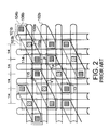
- cells are arranged with cell arrangement pattern of the known 1/4 pitch type folded bit line system for achieving the high density of the device region patterns.
- bit lines 102b are placed in a parallel direction while a plurality of word lines 101b are placed in a vertical direction in the same manner as the structure illustrated in Fig. 1.
- word lines 101b are crossed to each other.
- each of the device region patterns 100b is formed in a rectangular shape.
- both ends of the device region pattern 100b are perpendicularly shaped, as illustrated in Fig. 2.
- each of the device region patterns 100b has wiring patterns 104a in both ends and a wiring pattern 103a in a center portion.
- a capacitor contact 106b is arranged in each of the wiring patterns 104b in the device region pattern 100b while a bit contact 105b is arranged in the wiring pattern 103a on the bit line 102b in the device region pattern 100b.
- the wiring pattern 103b is patterned and arranged to connect the bit contact 105b with a diffusion layer.
- the wiring pattern 104b is patterned and arranged to connect the capacitor contact 106b with a diffusion layer.
- the device region patterns 100b are alternately arranged at every 1/4 pitch on the basis of the bit lines 102a.
- the device region patterns 113,114 and 115 are formed as illustrated in Fig. 2.
- the device region pattern 114 is closest to the device region pattern 113.
- a distance between the device region patterns 113 and 114 is equal to a space d while a distance between the device region patterns 113 and 115 is equal to a space d'.
- This space d' is considerably small in comparison with the space s illustrated in Fig. 1. Consequently, field integration is increased in the cell layout illustrated in Fig. 2.
- the cell size can be reduced in the cell layout of the 1/4 pitch.
- the diffusion layer is arranged with the minimum space same as the memory cell structure due to the cell structure of the 1/2 pitch type.
- a semiconductor memory device utilizes the known folded bit line system.
- bit lines are placed in a parallel direction while a plurality of word lines are placed in a vertical direction.
- bit lines and the word lines are perpendicularly crossed to each other.
- a plurality of device region patterns are arranged so as to cross the bit lines and the word lines.
- a separating distance between adjacent device region patterns is equal to a first space while a separating distance between closest portions of the adjacent device region patterns is equal to a second space.
- each of the device region patterns is inclined for the bit line with a predetermined angle so that the first space exceeds the second space.
- the device region pattern has first wiring patterns in both ends and a second wiring pattern in a center portion.
- a capacitor contact is arranged in each of the first wiring patterns while a bit contact is arranged in the second wiring pattern.
- the first space corresponds to a vertical distance between the capacitor contacts.
- the first wiring pattern is patterned and arranged so as to connect the capacitor contact with a first diffusion layer while the second wiring pattern is patterned and arranged so as to connect the bit contact with a second diffusion layer.
- the second space exceeds a predetermined minimum separating space.
- each of the device region patterns is inclined with the angle which is not exceeding approximately 26 degree.
- each of said device region patterns is inclined with the angle which is not exceeding approximately 13 degree.
- the device region patterns are alternately arranged at every 1/4 pitch on the basis of the bit line.
- each of the device region patterns is inclined for the bit line with the predetermined angle so that the first space exceeds the second space in this invention, as mentioned before.
- the separating distance of the device region pattern can be widened.
- the distance between the capacitor contacts can be widened. In consequence, the increase of the contact resistance can be suppressed, and the electrical characteristic is increased.
- the distance (space) between the capacitor contacts can be widened by adjusting the inclined angle as compared to the conventional 1/4 pitch type cell layout.
- the semiconductor memory device according to the first embodiment has cell arrangement pattern of the folded bit line system.
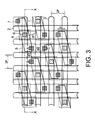
- bit lines 3 are placed in a parallel direction while a plurality of word lines 2 are placed in a vertical direction in the same manner as the structure illustrated in Fig. 2.
- bit lines 3 and the word lines 2 are crossed to each other.
- each of the device region patterns 1 is formed in a rectangular shape.
- both ends of the device region pattern 1 are perpendicularly shaped.
- the device region pattern 1 is inclined with an angle at which separating spaces d1 and d2 between the adjacent device region patterns exceed separating space d3 of the closest portion.
- each of the device region patterns 1 has wiring patterns 5 in both ends and a wiring pattern 4 in a center portion.
- a capacitor contact 7 is arranged in each of the wiring patterns 5 in the device region pattern 1 while a bit contact 6 is arranged in the wiring pattern 4 in the device region pattern 1.
- the wiring pattern 4 is patterned and arranged to connect the bit contact 6 with a diffusion layer.
- the wiring pattern 5 is patterned and arranged to connect the capacitor contact 7 with a diffusion layer.
- the device region patterns 1 are alternately arranged at every 1/4 pitch on the basis of the bit lines 3.
- each repeating pitch of the word lines 2 and the bit lines 3 is equal to 2F in such a memory cell structure.
- the cell having area of 8F 2 can be realized in the folded bit line system.
- the layout of the formable minimum cell can be obtained by setting the value F to the minimum distance.
- the device region pattern 1 is inclined for the bit line 3. Thereby, the separating space d1 between the adjacent device region patterns 1 exceeds the distance F.
- the wiring pattern 5 contacts with the diffusion layer at portions A and B illustrated in Fig. 3 in the device region pattern 1. Therefore, the portions A and B are most strict regions for electrically separating the device region patterns 1.
- the separating space d3 between the portions A and B is set to the minimum separating distance F in the normal 1/ 4 pitch type cell layout.
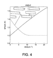
- the space (F) between the adjacent device region patterns 1 is illustrated by a solid line. Further, the space (F) between the diffusion layers, in which the capacitor contacts 7 are formed, is illustrated by the broken line.
- the device region pattern 1 is inclined with about 26 degree in the normal (conventional) 1/4 pitch type cell layout, the device region pattern 1 is inclined with 13 degree or less for the bit line 3 in the cell layout according to this invention. In this event, the separating space d3 between the portions A and B illustrated in Fig. 3 exceeds the minimum separating distance (F).
- the separating space between the portions A and C becomes the minimum distance in the normal (conventional) 1/4 pitch type cell layout.
- the separating space d2 between the portions A and C becomes considerably longer than the minimum separating distance (F) in the cell layout according to this invention, as illustrated in Fig. 3.
- the separating distances d1, d2 and d3 become substantially identical to each other in the case cell layout illustrated in Fig. 3.
- the separating distances d1, d2 and d3 of the device region patterns 1 can be widened. In consequence, an increase of contact resistance can be suppressed, and electrical characteristic is increased.
- the cell size can become small. Consequently, integration can be further achieved with high density.
- a gate oxide film 11 and a device separating oxide film 12 are formed on a surface of a silicon substrate 10. Further, a gate lower electrode 13 is formed on the gate oxide film 11.
- the gate lower electrode 13 is formed by polysilicon and has a thickness of 100 nm.
- a gate upper electrode 14 is formed on the gate lower electrode 13.
- the gate upper electrode 14 is formed by WSi and has a thickness of 100 nm.
- the word line 2 illustrated in Fig. 3 is formed by these two electrodes 13 and 14.
- a gate insulating film 15 having a thickness of about 80 nm is formed on the gate upper electrode 14. Further, a gate sidewall insulating film 16 having a thickness of about 50 nm is formed on a side surface of the gate lower electrode 13, the gate upper electrode 14 and the gate insulating film 15.
- the wiring pattern 4 for the bit contact 6 and the wiring pattern 5 for the capacitor contact 7 are electrically insulated by the gate sidewall insulating film 16.
- the bit contact 6 is placed on the wiring pattern 4 so as to be insulated by a first interlayer insulating film 17.
- the capacitor contact 7 is placed on the wiring pattern 5 so that the capacitor contact 7 is insulated by the first interlayer insulating film 17 under the bit line 3 and is insulated by a second interlayer insulating film 18 over the bit line 3.
- a surface of a capacitor lower electrode 19 is coated by a capacitor insulating film 20, and a capacitor upper electrode 21 is placed thereon.
- the wiring pattern 4 for bit contact 6 and the wiring pattern 5 for the capacitor contact 7 are not arranged different from the first example illustrated in Fig. 3.
- the device region pattern 1 has the capacitor contacts 7 at the both ends and the bit contact 6 at the center portion in the memory cell structure.
- the device region pattern 1 is inclined with the same angle as the first embodiment illustrated in Fig. 3 for the bit line 3.
- the diffusion layer 32 which contacts with the capacitor contact 7 is bent and extended in the direction parallel to the word line 2 different from the first embodiment.
- the diffusion layer 32 for forming the capacitor contact 7 can be enlarged as compared to the conventional 1/4 pitch type cell layout. Consequently, alignment margin of the capacitor contact 7 and the device region pattern 1 becomes large.
- the separating distance d from the bit contact 6' to the adjacent device region pattern 1 exceeds the minimum separating distance (F).
- the device region (namely, the diffusion layer 32) for forming the capacitor contact 7 becomes large.
- the contact resistance can be reduced, as mentioned before.
- shrinkage in a long side direction becomes remarkable with respect to a narrow and long pattern, such as, the device region pattern 1.
- each device region pattern 113, 114, and 115 is shrunk in the conventional 1/4 pitch type cell layout illustrated in Fig. 2.
- the diffusion layer does not sufficiently extend in the direction parallel to word line 101b, and further, alignment deviation also occurs. Thereby, the diffusion layer for the capacitor contact 106b may not be formed in the worst case.
- this problem can be solved by adopting the cell layout illustrated in Fig. 4.
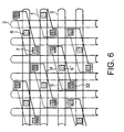
- the wiring pattern 4 for the bit contact 6 and the wiring pattern 5 for the capacitor contact 7 are arranged, like the first embodiment.
- the device region pattern 1 has the capacitor contacts 7 at the both ends and the bit contact 6 at the center portion in the memory cell structure.
- the device region pattern 1 is inclined with the same angle as the first embodiment illustrated in Fig. 2 for the bit line 3.
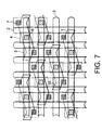
- a space between adjacent capacitor contacts 7 is further widened in the third embodiment, different from the first embodiment. Namely, a diffusion layer 33 is bent and extended in a predetermined direction, as illustrated in Fig. 7. Consequently, even when the device region pattern 1 is extended in a long side direction, the device region pattern 1 does not almost contacts with the other device region pattern 1.
- the diffusion layer 33 is bent and extended in the third embodiment. Thereby, even when the shrinkage and the alignment deviation of the resist pattern occurs, the diffusion layer 33 for forming the capacitor contact 7 can be sufficiently formed.
Landscapes
- Semiconductor Memories (AREA)
Applications Claiming Priority (2)
| Application Number | Priority Date | Filing Date | Title |
|---|---|---|---|
| JP10097801A JP3137185B2 (ja) | 1998-04-09 | 1998-04-09 | 半導体記憶装置 |
| JP9780198 | 1998-04-09 |
Publications (2)
| Publication Number | Publication Date |
|---|---|
| EP0949681A1 true EP0949681A1 (fr) | 1999-10-13 |
| EP0949681B1 EP0949681B1 (fr) | 2002-09-04 |
Family
ID=14201895
Family Applications (1)
| Application Number | Title | Priority Date | Filing Date |
|---|---|---|---|
| EP99107025A Expired - Lifetime EP0949681B1 (fr) | 1998-04-09 | 1999-04-09 | Dispositif de mémoire semiconductrice |
Country Status (6)
| Country | Link |
|---|---|
| US (1) | US6185120B1 (fr) |
| EP (1) | EP0949681B1 (fr) |
| JP (1) | JP3137185B2 (fr) |
| KR (1) | KR100332012B1 (fr) |
| CN (1) | CN1126176C (fr) |
| DE (1) | DE69902712T2 (fr) |
Cited By (1)
| Publication number | Priority date | Publication date | Assignee | Title |
|---|---|---|---|---|
| US10872858B2 (en) | 2017-08-30 | 2020-12-22 | United Microelectronics Corp. | Semiconductor memory device |
Families Citing this family (12)
| Publication number | Priority date | Publication date | Assignee | Title |
|---|---|---|---|---|
| JP4063450B2 (ja) * | 1999-06-14 | 2008-03-19 | エルピーダメモリ株式会社 | 半導体集積回路装置 |
| US6522579B2 (en) * | 2001-01-24 | 2003-02-18 | Infineon Technologies, Ag | Non-orthogonal MRAM device |
| US6549476B2 (en) * | 2001-04-09 | 2003-04-15 | Micron Technology, Inc. | Device and method for using complementary bits in a memory array |
| KR100401513B1 (ko) * | 2001-06-29 | 2003-10-17 | 주식회사 하이닉스반도체 | 반도체 소자의 배선 형성방법 |
| KR100891249B1 (ko) * | 2002-05-31 | 2009-04-01 | 주식회사 하이닉스반도체 | 6f2 dram 셀을 구비한 반도체 메모리 소자 |
| KR100574981B1 (ko) | 2004-05-31 | 2006-05-02 | 삼성전자주식회사 | 트랜지스터의 리세스 채널을 위한 트렌치를 형성하는 방법및 이를 위한 레이아웃 |
| KR100720251B1 (ko) | 2005-12-30 | 2007-05-22 | 주식회사 하이닉스반도체 | 노광 마스크 및 이를 이용한 반도체 소자의 제조방법 |
| JP5694625B2 (ja) | 2006-04-13 | 2015-04-01 | ピーエスフォー ルクスコ エスエイアールエルPS4 Luxco S.a.r.l. | 半導体記憶装置 |
| JP2010161173A (ja) * | 2009-01-07 | 2010-07-22 | Renesas Electronics Corp | 半導体記憶装置 |
| KR101102764B1 (ko) * | 2009-07-31 | 2012-01-03 | 주식회사 하이닉스반도체 | 반도체 소자의 레이아웃 및 반도체 소자의 형성방법 |
| US10818729B2 (en) * | 2018-05-17 | 2020-10-27 | Macronix International Co., Ltd. | Bit cost scalable 3D phase change cross-point memory |
| CN112366203B (zh) * | 2020-10-23 | 2023-01-03 | 福建省晋华集成电路有限公司 | 图案布局以及其形成方法 |
Citations (3)
| Publication number | Priority date | Publication date | Assignee | Title |
|---|---|---|---|---|
| EP0399531A1 (fr) * | 1989-05-23 | 1990-11-28 | Kabushiki Kaisha Toshiba | Dispositif semi-conducteur à mémoire |
| EP0428247A2 (fr) * | 1989-08-19 | 1991-05-22 | Fujitsu Limited | Dispositif semi-conducteur à mÀ©moire comprenant une disposition de contacts améliorée |
| EP0464251A1 (fr) * | 1990-07-06 | 1992-01-08 | Fujitsu Limited | Mémoire dynamique à accès aléatoire ayant un agencement amélioré et procédé d'arranger la configuration des cellules de mémoire |
Family Cites Families (10)
| Publication number | Priority date | Publication date | Assignee | Title |
|---|---|---|---|---|
| US5194752A (en) * | 1989-05-23 | 1993-03-16 | Kabushiki Kaisha Toshiba | Semiconductor memory device |
| JP3013458B2 (ja) | 1990-02-26 | 2000-02-28 | 日本電気株式会社 | 半導体記憶装置 |
| JP3344485B2 (ja) | 1990-11-09 | 2002-11-11 | 富士通株式会社 | 半導体装置の製造方法 |
| JP2825031B2 (ja) | 1991-08-06 | 1998-11-18 | 日本電気株式会社 | 半導体メモリ装置 |
| JP3072675B2 (ja) | 1992-05-15 | 2000-07-31 | 株式会社明電舎 | 空間フィルタを用いた移動距離測定装置 |
| JP3179638B2 (ja) | 1993-10-25 | 2001-06-25 | 日本電信電話株式会社 | 光学素子の形成方法 |
| JPH0878640A (ja) | 1994-08-31 | 1996-03-22 | Nippon Steel Corp | 半導体記憶装置及びその製造方法 |
| JP3520144B2 (ja) | 1995-10-26 | 2004-04-19 | 株式会社ルネサステクノロジ | 半導体記憶装置およびその製造方法 |
| JP2950265B2 (ja) * | 1996-07-30 | 1999-09-20 | 日本電気株式会社 | 半導体記憶装置 |
| US6060351A (en) * | 1997-12-24 | 2000-05-09 | Micron Technology, Inc. | Process for forming capacitor over bit line memory cell |
-
1998
- 1998-04-09 JP JP10097801A patent/JP3137185B2/ja not_active Expired - Fee Related
-
1999
- 1999-04-07 US US09/287,516 patent/US6185120B1/en not_active Expired - Fee Related
- 1999-04-08 CN CN99105496A patent/CN1126176C/zh not_active Expired - Fee Related
- 1999-04-09 KR KR1019990012486A patent/KR100332012B1/ko not_active Expired - Fee Related
- 1999-04-09 EP EP99107025A patent/EP0949681B1/fr not_active Expired - Lifetime
- 1999-04-09 DE DE69902712T patent/DE69902712T2/de not_active Expired - Fee Related
Patent Citations (3)
| Publication number | Priority date | Publication date | Assignee | Title |
|---|---|---|---|---|
| EP0399531A1 (fr) * | 1989-05-23 | 1990-11-28 | Kabushiki Kaisha Toshiba | Dispositif semi-conducteur à mémoire |
| EP0428247A2 (fr) * | 1989-08-19 | 1991-05-22 | Fujitsu Limited | Dispositif semi-conducteur à mÀ©moire comprenant une disposition de contacts améliorée |
| EP0464251A1 (fr) * | 1990-07-06 | 1992-01-08 | Fujitsu Limited | Mémoire dynamique à accès aléatoire ayant un agencement amélioré et procédé d'arranger la configuration des cellules de mémoire |
Cited By (1)
| Publication number | Priority date | Publication date | Assignee | Title |
|---|---|---|---|---|
| US10872858B2 (en) | 2017-08-30 | 2020-12-22 | United Microelectronics Corp. | Semiconductor memory device |
Also Published As
| Publication number | Publication date |
|---|---|
| JPH11297954A (ja) | 1999-10-29 |
| US6185120B1 (en) | 2001-02-06 |
| CN1231514A (zh) | 1999-10-13 |
| CN1126176C (zh) | 2003-10-29 |
| DE69902712D1 (de) | 2002-10-10 |
| KR19990083078A (ko) | 1999-11-25 |
| DE69902712T2 (de) | 2003-08-07 |
| JP3137185B2 (ja) | 2001-02-19 |
| EP0949681B1 (fr) | 2002-09-04 |
| KR100332012B1 (ko) | 2002-04-10 |
Similar Documents
| Publication | Publication Date | Title |
|---|---|---|
| JP3368002B2 (ja) | 半導体記憶装置 | |
| US6410948B1 (en) | Memory cell arrays comprising intersecting slanted portions | |
| US5578847A (en) | Dynamic semiconductor memory device with higher density bit line/word line layout | |
| US5378906A (en) | Dynamic random access memory having improved layout | |
| US6809364B2 (en) | Semiconductor integrated circuit device and a method of manufacture thereof | |
| JP2990870B2 (ja) | 半導体集積回路装置及びその製造方法 | |
| JP2803712B2 (ja) | 半導体記憶装置 | |
| US6185120B1 (en) | Semiconductor memory device | |
| KR20210018683A (ko) | 지지 패턴을 포함하는 반도체 소자 및 이의 제조 방법 | |
| US5597763A (en) | Method for manufacturing a semiconductor wiring structure including a self-aligned contact hole | |
| JP3397809B2 (ja) | 半導体メモリセルの製造方法 | |
| US5959319A (en) | Semiconductor memory device having word line conductors provided at lower level than memory cell capacitor and method of manufacturing same | |
| US5153689A (en) | Semiconductor memory device having bit lines formed of an interconnecting layer of lower reflectance material than the material of the word lines | |
| JPH0936325A (ja) | 半導体集積回路装置 | |
| US5501999A (en) | Process for formation of capacitor for DRAM cell | |
| US6839264B2 (en) | Semiconductor device without adverse effects caused by inclinations of word line and bit line | |
| US6104050A (en) | Methods for fabricating integrated circuit devices including etching barrier layers and related structures | |
| JPH098252A (ja) | 半導体記憶装置及びその製造方法 | |
| JP3202501B2 (ja) | 半導体記憶装置及びその製造方法 | |
| JP3087712B2 (ja) | 半導体記憶装置 | |
| KR100330716B1 (ko) | 도전층 패턴과 그 하부 콘택홀 간의 얼라인먼트 마진을개선할수 있는 반도체 장치의 패턴 레이아웃 구조 | |
| JP3165693B2 (ja) | スタックトキャパシタ型dram | |
| US6278151B1 (en) | Semiconductor device having wiring detour around step | |
| KR100207505B1 (ko) | 반도체 메모리장치 및 그 제조방법 | |
| JP3189807B2 (ja) | 半導体装置の製造方法 |
Legal Events
| Date | Code | Title | Description |
|---|---|---|---|
| PUAI | Public reference made under article 153(3) epc to a published international application that has entered the european phase |
Free format text: ORIGINAL CODE: 0009012 |
|
| 17P | Request for examination filed |
Effective date: 19990817 |
|
| AK | Designated contracting states |
Kind code of ref document: A1 Designated state(s): DE GB |
|
| AX | Request for extension of the european patent |
Free format text: AL;LT;LV;MK;RO;SI |
|
| AKX | Designation fees paid |
Free format text: DE GB |
|
| 17Q | First examination report despatched |
Effective date: 20000929 |
|
| GRAG | Despatch of communication of intention to grant |
Free format text: ORIGINAL CODE: EPIDOS AGRA |
|
| GRAG | Despatch of communication of intention to grant |
Free format text: ORIGINAL CODE: EPIDOS AGRA |
|
| GRAH | Despatch of communication of intention to grant a patent |
Free format text: ORIGINAL CODE: EPIDOS IGRA |
|
| GRAH | Despatch of communication of intention to grant a patent |
Free format text: ORIGINAL CODE: EPIDOS IGRA |
|
| GRAA | (expected) grant |
Free format text: ORIGINAL CODE: 0009210 |
|
| AK | Designated contracting states |
Kind code of ref document: B1 Designated state(s): DE GB |
|
| REG | Reference to a national code |
Ref country code: GB Ref legal event code: FG4D |
|
| REF | Corresponds to: |
Ref document number: 69902712 Country of ref document: DE Date of ref document: 20021010 |
|
| REG | Reference to a national code |
Ref country code: GB Ref legal event code: 732E |
|
| PLBE | No opposition filed within time limit |
Free format text: ORIGINAL CODE: 0009261 |
|
| STAA | Information on the status of an ep patent application or granted ep patent |
Free format text: STATUS: NO OPPOSITION FILED WITHIN TIME LIMIT |
|
| 26N | No opposition filed |
Effective date: 20030605 |
|
| PGFP | Annual fee paid to national office [announced via postgrant information from national office to epo] |
Ref country code: GB Payment date: 20040407 Year of fee payment: 6 |
|
| PGFP | Annual fee paid to national office [announced via postgrant information from national office to epo] |
Ref country code: DE Payment date: 20040422 Year of fee payment: 6 |
|
| PG25 | Lapsed in a contracting state [announced via postgrant information from national office to epo] |
Ref country code: GB Free format text: LAPSE BECAUSE OF NON-PAYMENT OF DUE FEES Effective date: 20050409 |
|
| PG25 | Lapsed in a contracting state [announced via postgrant information from national office to epo] |
Ref country code: DE Free format text: LAPSE BECAUSE OF NON-PAYMENT OF DUE FEES Effective date: 20051101 |
|
| GBPC | Gb: european patent ceased through non-payment of renewal fee |
Effective date: 20050409 |