EP0949694A2 - Magnetowiderstand mit geordneter Doppelperovskitestruktur und deren Herstellungsverfahren - Google Patents
Magnetowiderstand mit geordneter Doppelperovskitestruktur und deren Herstellungsverfahren Download PDFInfo
- Publication number
- EP0949694A2 EP0949694A2 EP99302347A EP99302347A EP0949694A2 EP 0949694 A2 EP0949694 A2 EP 0949694A2 EP 99302347 A EP99302347 A EP 99302347A EP 99302347 A EP99302347 A EP 99302347A EP 0949694 A2 EP0949694 A2 EP 0949694A2
- Authority
- EP
- European Patent Office
- Prior art keywords
- atoms
- magnetoresistor
- double perovskite
- oxide
- temperature
- Prior art date
- Legal status (The legal status is an assumption and is not a legal conclusion. Google has not performed a legal analysis and makes no representation as to the accuracy of the status listed.)
- Granted
Links
Images




Classifications
-
- H—ELECTRICITY
- H10—SEMICONDUCTOR DEVICES; ELECTRIC SOLID-STATE DEVICES NOT OTHERWISE PROVIDED FOR
- H10N—ELECTRIC SOLID-STATE DEVICES NOT OTHERWISE PROVIDED FOR
- H10N50/00—Galvanomagnetic devices
- H10N50/80—Constructional details
- H10N50/85—Materials of the active region
-
- B—PERFORMING OPERATIONS; TRANSPORTING
- B82—NANOTECHNOLOGY
- B82Y—SPECIFIC USES OR APPLICATIONS OF NANOSTRUCTURES; MEASUREMENT OR ANALYSIS OF NANOSTRUCTURES; MANUFACTURE OR TREATMENT OF NANOSTRUCTURES
- B82Y15/00—Nanotechnology for interacting, sensing or actuating, e.g. quantum dots as markers in protein assays or molecular motors
-
- H—ELECTRICITY
- H01—ELECTRIC ELEMENTS
- H01F—MAGNETS; INDUCTANCES; TRANSFORMERS; SELECTION OF MATERIALS FOR THEIR MAGNETIC PROPERTIES
- H01F1/00—Magnets or magnetic bodies characterised by the magnetic materials therefor; Selection of materials for their magnetic properties
- H01F1/01—Magnets or magnetic bodies characterised by the magnetic materials therefor; Selection of materials for their magnetic properties of inorganic materials
- H01F1/40—Magnets or magnetic bodies characterised by the magnetic materials therefor; Selection of materials for their magnetic properties of inorganic materials of magnetic semiconductor materials, e.g. CdCr2S4
- H01F1/401—Magnets or magnetic bodies characterised by the magnetic materials therefor; Selection of materials for their magnetic properties of inorganic materials of magnetic semiconductor materials, e.g. CdCr2S4 diluted
- H01F1/407—Diluted non-magnetic ions in a magnetic cation-sublattice, e.g. perovskites, La1-x(Ba,Sr)xMnO3
Definitions
- the present invention relates to a magnetoresistive element (magnetoresistor) with an ordered double perovskite structure and a method for producing the same. More particularly, the present invention relates to a magnetoresistor which is an oxide crystal with on ordered double perovskite crystal structure, that has electrical conductivity, is enhanced in magnetic-conductance and spin-polarisation characteristics, and is advantageously usable as a probe of a spin-polarisation scanning type tunneling microscope or a magnetoresistor operable at room temperature, and to a method for the production of the oxide crystal.
- an oxide with an ordered double perovskite type structure represented by the chemical formula of Sr 2 FeMoO 6 or Sr 2 FeReO 6 .
- the crystal structure, magnetic property, etc. thereof have been studied, and it has been reported that the curie temperature thereof is in the vicinity of 400 K that is much higher than room temperature.
- the oxide manifests a negative huge magnetoresistive effect.
- the present invention has been proposed in view of the above.
- An object of the present invention is to provide a magnetoresistor that manifests a magnetoresistive effect over an entire temperature range.
- Another object of the present invention is to provide a method for producing the magnetoresistor more easily than a conventional single-crystal producing method.
- the present invention provides a magnetoresistor with an ordered double perovskite structure that is an oxide crystal which has an ordered double perovskite crystal structure represented by the general formula of A 2 BB'O 6 , wherein A stands for Sr atoms, B for Fe atoms and B' for Mo or Re atoms, the magnetoresistor being characterised in that the Fe atoms and the Mo or Re atoms are alternately arranged and that the oxide crystal exhibits negative magnetoresistive characteristics.
- the Fe atoms and the Mo or Re atoms have a degree of alternate arrangement that is not less than 20%.
- the present invention also provides a method for producing a magnetoresistor that is an oxide crystal having an ordered double perovskite crystal structure represented by a composition of Sr 2 FeReO 6 , comprising the steps of weighing, mixing and forming raw material powders in a glove compartment to obtain a desired shaped article having the composition, and calcining, sintering and heat-treating the article, the method being characterised in that the calcining and sintering steps are taken in an evacuated sealed capsule at temperatures of about 900°C and of not less than 1100°C, respectively, and heat-treating step is taken a stream of inert gas at a temperature of not less than 1125°C.
- the inventors made various studies on perovskite oxide crystals and found a rare phenomenon that occurred in an oxide ceramic. That is to say, in an oxide crystal having an ordered double perovskite crystal structure represented by the chemical formula of Sr 2 FeMoO 6 or Sr 2 FeReO 6 , a negative huge magnetoresistive effect is manifested over an entire temperature range of not more than the vicinity of room temperature to 4 K. This invention has been perfected as the result of this knowledge.
- the inventors also made studies on a method for producing an oxide having an ordered double perovskite crystal structure represented by the chemical formula of Sr 2 FeMoO 6 . As a result, they found that the oxide manifested a negative huge magnetoresistive effect when produced by weighing and mixing raw oxide materials into an article having a desired composition, calcining the article at a temperature of approximately 900°C, primarily sintering the calcined article in a reducing atmosphere at a temperature of 1100°C to 1300°C for 1 hour to 20 hours.
- the inventors found that the oxide obtained by weighing, mixing and forming raw oxide materials within a glove compartment to obtain a desired shaped article having the composition, sealing the article in an evacuated silica capsule, effecting calcining treatment at about 900°C and primary sintering treatment at not less than 1100°C of the article in the silica capsule, and heat-treating the resultant article in a stream of inert gas such as highly pure argon gas at not less than 1125°C manifested a negative huge magnetoresistive characteristic over an entire temperature range of not more than room temperature.
- inert gas such as highly pure argon gas at not less than 1125°C manifested a negative huge magnetoresistive characteristic over an entire temperature range of not more than room temperature.
- the present invention provides a magnetoresistor with an ordered double perovskite crystal structure, that is an oxide crystal which has an ordered double perovskite crystal structure represented by the general formula of A 2 BB'O 6 wherein A stands for Sr atoms, B for Fe atoms and B' for Mo or Re atoms and wherein the Fe atoms and the Mo or Re atoms are alternately arranged, which exhibits negative magnetoresistive characteristics, which has a magnetic transition temperature that is higher than room temperature, which has an electronic structure exhibiting a spin-polarisation rate of 100% at a cryogenic temperature and a magnetoresistive effect at an entire temperature of room temperature to a cryogenic temperature, which is a polycrystal easier to produce in comparison with a conventional manganese oxide single crystal, and which is put to practical use with considerable effectiveness as a magnetic sensor operable at room temperature, a probe of a spin-polarisation scanning type tunneling microscope, etc,
- the disc thus obtained was calcined at 900°C for 3 hours and then cooled to room temperature.
- the resultant disc was pulverised minutely and then re-molded into a second disc 10 mm in diameter and 1 mm in thickness under a pressure of about 0.3 ton to 1.0 ton/cm 2 .
- the second disc was sintered at 1150°C in a stream of argon gas containing 7% of H 2 gas for 2 hours, then cooled to room temperature, thereafter taken out, and cut into square pole samples measuring about 1 mm x 1 mm x 5 mm for measurement of electroresistivity.
- a polycrystal oxide ceramic sample was assayed for temperature dependency of electroresistivity using the direct-current four-terminal method to obtain metallic results as shown in Figure 3.
- the results were that the samples had a 32% resistivity (4.2 K) and a 3.5% resistivity (300 K), respectively.
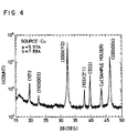
- the relative strength of the X-ray diffraction peak indexed as (101) to the maximum X-ray diffraction peak indexed as (200)(112) indicates a degree of alternate arrangement of the Fe atoms and the Mo atoms.
- the relative strength ratio of the peak (101) to the peak (200)(112) was 100 : 4.8 (4.8%).
- This relative strength ratio and the magnetoresistive effect have a correlation.
- the ratio was 100 : 2.1 (a 42% degree of alternate arrangement)
- the magnetoresistive effect obtained from equation (1) at 4.2 K was 44%.
- the ratio was 100 : 1.3 (a 27% degree of alternate arrangement)
- the effect obtained from equation (1) at 4.2 K was 19%.
- the ratio was 100 : 0.9 (a 19% degree of alternate arrangement)
- the effect obtained from equation (1) at 4.2 K was 10%.
- the second disc obtained in Working Example 1 was sintered at 1300°C in a stream of argon gas containing 7% of H 2 gas for 25 hours.
- the sintered article obtained did not have a magnetoresistive effect.
- the sintering time was set to be not more than 1 hour, the sintered article obtained had insufficient strength.
- the disc thus obtained was immediately sealed in an evacuted silica capsule, calcined at 900°C for 3 hours, then cooled to room temperature, thereafter pulverised minutely, and re-molded under a pressure of about 0.3 ton to 1.0 ton/cm 2 into a second disc 10 mm in diameter and 1 mm in thickness.
- the second disc was immediately sealed in the evacuated silica capsule, sintered at 1200°C for 3 hours, cooled to room temperature, and taken out.
- the resultant disc was heat-treated at 1200°C in a stream of argon gas for 3 hours, and cut into square pole samples measuring about 1 mm x 1 mm x 5 mm for measurement of electroresistivity.
- a polycrystal oxide ceramic sample was assayed for temperature dependency of electroresistivity using the direct-current four-terminal method. As shown in Figure 8, there was observed a negative magnetoresistive effect over a temperature range of not more than room temperature to 2 K wherein the resistivity decreased with an increasing magnetic field applied.
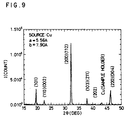
- the relative strength ratio of the X-ray diffraction peak indexed as (101) to the maximum X-ray diffraction peak indexed as (200)(112) indicates a degree of alternate arrangement of the Fe atoms and the Re atoms in the ordered double perovskite structure.
- the powder X-ray diffraction results shown in Figure 9 was subjected to the Rietveld analysis to find that a degree of alternate arrangement of the Fe atoms and the Re atoms in the structure was 97%.
- the relative strength ratio of the peak (101) to the peak (200)(112) obtained by the Rietveld analysis was 100 : 25 (25%). This relative strength ratio and the magnetoresistive effect had a correlation.
- the magnetoresistive effect at 4.2 K obtained from equation (2) was 9.5%.
- the magnetoresistive effect at 4.2 K obtained from equation (2) was 5.3%.
- the magnetoresistive effect at 4.2 K obtained from equation (2) was 3.8%.
- the article obtained in Working Example 2 was heat-treated at not more than 1125°C in a stream of inert gas.
- the resultant article did not have a negative huge magnetoresistive effect in an entire temperature range of not more than room temperature.
- the calcining and primary sintering treatments were effected without sealing the article in an evacuated silica capsule, the sample obtained had a composition different from a target one.
Landscapes
- Engineering & Computer Science (AREA)
- Chemical & Material Sciences (AREA)
- Nanotechnology (AREA)
- Materials Engineering (AREA)
- Molecular Biology (AREA)
- General Health & Medical Sciences (AREA)
- Crystallography & Structural Chemistry (AREA)
- Life Sciences & Earth Sciences (AREA)
- Health & Medical Sciences (AREA)
- Power Engineering (AREA)
- Compounds Of Iron (AREA)
- Compositions Of Oxide Ceramics (AREA)
- Hard Magnetic Materials (AREA)
- Hall/Mr Elements (AREA)
- Inorganic Compounds Of Heavy Metals (AREA)
- Crystals, And After-Treatments Of Crystals (AREA)
Applications Claiming Priority (4)
| Application Number | Priority Date | Filing Date | Title |
|---|---|---|---|
| JP10081284A JP2981661B2 (ja) | 1998-03-27 | 1998-03-27 | 二重整列ペロブスカイト構造磁気抵抗素子 |
| JP8128498 | 1998-03-27 | ||
| JP29581098 | 1998-10-16 | ||
| JP10295810A JP3010203B1 (ja) | 1998-10-16 | 1998-10-16 | 二重整列ペロブスカイト構造磁気抵抗素子及びその製造方法 |
Publications (3)
| Publication Number | Publication Date |
|---|---|
| EP0949694A2 true EP0949694A2 (de) | 1999-10-13 |
| EP0949694A3 EP0949694A3 (de) | 2003-11-26 |
| EP0949694B1 EP0949694B1 (de) | 2008-01-09 |
Family
ID=26422317
Family Applications (1)
| Application Number | Title | Priority Date | Filing Date |
|---|---|---|---|
| EP99302347A Expired - Lifetime EP0949694B1 (de) | 1998-03-27 | 1999-03-26 | Anwendung von einem Magnetowiderstand mit geordneter Doppelperovskitestruktur und deren Herstellungsverfahren |
Country Status (4)
| Country | Link |
|---|---|
| US (1) | US6137395A (de) |
| EP (1) | EP0949694B1 (de) |
| AT (1) | ATE383663T1 (de) |
| DE (1) | DE69937921T2 (de) |
Cited By (1)
| Publication number | Priority date | Publication date | Assignee | Title |
|---|---|---|---|---|
| WO2001033585A1 (en) * | 1999-11-05 | 2001-05-10 | Oxxel Oxide Electronics Technology, Inc. | Synthesis and magnetoresistance test system using double-perovskite samples for preparation of a magnetoresistance device |
Families Citing this family (4)
| Publication number | Priority date | Publication date | Assignee | Title |
|---|---|---|---|---|
| JP2001085218A (ja) * | 1999-09-17 | 2001-03-30 | Sharp Corp | 強磁性金属酸化物多結晶体及びその製造方法 |
| DE102008009817A1 (de) * | 2008-02-19 | 2009-08-27 | Epcos Ag | Verbundwerkstoff zur Temperaturmessung, Temperatursensor aufweisend den Verbundwerkstoff und Verfahren zur Herstellung des Verbundwerkstoffs und des Temperatursensors |
| CN112094104B (zh) * | 2020-09-23 | 2023-03-28 | 齐齐哈尔大学 | 一种双钙钛矿型自旋电子学材料及其制备方法 |
| CN114042459B (zh) * | 2021-11-22 | 2024-01-05 | 合肥学院 | 一种类树状软磁性Sr2FeMoO6高效可见光催化剂的制备方法 |
Family Cites Families (2)
| Publication number | Priority date | Publication date | Assignee | Title |
|---|---|---|---|---|
| FR2165206A5 (de) * | 1971-12-22 | 1973-08-03 | Cii | |
| JP3345072B2 (ja) * | 1993-02-09 | 2002-11-18 | 株式会社日立製作所 | 磁気抵抗効果素子および磁気記録再生装置 |
-
1999
- 1999-03-26 AT AT99302347T patent/ATE383663T1/de not_active IP Right Cessation
- 1999-03-26 EP EP99302347A patent/EP0949694B1/de not_active Expired - Lifetime
- 1999-03-26 DE DE69937921T patent/DE69937921T2/de not_active Expired - Lifetime
- 1999-03-26 US US09/277,223 patent/US6137395A/en not_active Expired - Fee Related
Non-Patent Citations (3)
| Title |
|---|
| HWANG H Y ET AL: "Spin-polarized intergrain tunneling in La/sub 2/3/Sr/sub 1/3/MnO/sub 3/" PHYSICAL REVIEW LETTERS, 2 SEPT. 1996, APS, USA, vol. 77, no. 10, pages 2041-2044, XP002255894 ISSN: 0031-9007 * |
| ITOH M ET AL: "Valency pair and properties of 1:1 ordered perovskite-type compounds Sr2MMoO6 (M = Mn,Fe,Co)" MATERIALS SCIENCE AND ENGINEERING B, ELSEVIER SEQUOIA, LAUSANNE, CH, vol. 41, no. 1, 1 October 1996 (1996-10-01), pages 55-58, XP004077876 ISSN: 0921-5107 * |
| KOBAYASHI K -I ET AL: "Room-temperature magnetoresistance in an oxide material with an ordered double-perovskite structure" NATURE, 15 OCT. 1998, MACMILLAN MAGAZINES, UK, vol. 395, no. 6703, pages 677-680, XP002255893 ISSN: 0028-0836 * |
Cited By (1)
| Publication number | Priority date | Publication date | Assignee | Title |
|---|---|---|---|---|
| WO2001033585A1 (en) * | 1999-11-05 | 2001-05-10 | Oxxel Oxide Electronics Technology, Inc. | Synthesis and magnetoresistance test system using double-perovskite samples for preparation of a magnetoresistance device |
Also Published As
| Publication number | Publication date |
|---|---|
| US6137395A (en) | 2000-10-24 |
| EP0949694A3 (de) | 2003-11-26 |
| EP0949694B1 (de) | 2008-01-09 |
| DE69937921D1 (de) | 2008-02-21 |
| DE69937921T2 (de) | 2009-01-02 |
| ATE383663T1 (de) | 2008-01-15 |
Similar Documents
| Publication | Publication Date | Title |
|---|---|---|
| Raphael et al. | Magnetic, structural, and transport properties of thin film and single crystal Co 2 MnSi | |
| Dabrowski et al. | Structure-properties phase diagram for La 1− x Sr x MnO 3 (0.1<~ x<~ 0. 2) | |
| Tegel et al. | Structural and magnetic phase transitions in the ternary iron arsenides SrFe2As2 and EuFe2As2 | |
| JP2685721B2 (ja) | 無粒界型マンガン酸化物系結晶体及びスイッチング型磁気抵抗素子 | |
| Troyanchuk et al. | Magnetotransport phenomena in A (Mn 3− x Cu x) Mn 4 O 12 (A= Ca, Tb, Tm) perovskites | |
| Hakeem | Room-temperature ferromagnetism in Zn1− xMnxO | |
| EP0949694B1 (de) | Anwendung von einem Magnetowiderstand mit geordneter Doppelperovskitestruktur und deren Herstellungsverfahren | |
| Bose et al. | Magnetocaloric properties of the La0. 7− xYxSr0. 3MnO3 giant magnetoresistance ceramics | |
| EP0732430B1 (de) | Einkristall auf Manganoxidbasis mit laminarer Struktur und Verfahren zu seiner Herstellung. | |
| Zandbergen et al. | Atomic structure and microstructure of very thin films of La0. 73Ca0. 27MnO3 on SrTiO3 | |
| Huang et al. | Granular Fe–Pb–O films with large tunneling magnetoresistance | |
| Moualhi et al. | Investigation of the structural, magnetic, and electrical characteristics of the La 0.7 Sr 0.25 Na 0.05 Mn 0.8 Ti 0.2 O 3 | |
| JP2674683B2 (ja) | メモリースイッチング型磁気抵抗素子 | |
| Wen-xu et al. | Effect of Fe doping in La 1− x Sr x MnO 3 | |
| Gritzner et al. | Preparation and properties of La0. 67Pb0. 33 (Mn1-xFex) O3 compounds | |
| Vijayanandhini et al. | Effects of Zn substitution on the magnetic and transport properties of La0. 6Sr0. 4Mn1− yZnyO3− δ (0≤ y≤ 0.3) | |
| Suzuki et al. | Structure and properties of layered perovskite compounds [Sr2VO4− δ] | |
| JP2812913B2 (ja) | 無粒界型マンガン酸化物系結晶体及び低磁場感応性磁気抵抗素子 | |
| JP3010203B1 (ja) | 二重整列ペロブスカイト構造磁気抵抗素子及びその製造方法 | |
| Khartsev et al. | Giant magnetoresistance of La 0.5 Pb 0.2 Ca 0.2 Y 0.1 MnO 3− δ films obtained by magnetron sputtering | |
| US6638442B1 (en) | Polycrystalline ferromagnetic metal oxide and method of manufacturing the same | |
| JP2981661B2 (ja) | 二重整列ペロブスカイト構造磁気抵抗素子 | |
| Singh et al. | Physical properties optimization of polycrystalline LiFeAs | |
| Powell et al. | Magnetic and electronic properties of lead-doped lanthanum manganate | |
| Kucherenko et al. | Influence of pressure, temperature, and magnetic field on the resistivity and magnetoresistive effect of lanthanum manganite ceramics and films with the composition La 0.7 Mn 1.3 O 3±δ |
Legal Events
| Date | Code | Title | Description |
|---|---|---|---|
| PUAI | Public reference made under article 153(3) epc to a published international application that has entered the european phase |
Free format text: ORIGINAL CODE: 0009012 |
|
| AK | Designated contracting states |
Kind code of ref document: A2 Designated state(s): AT BE CH CY DE DK ES FI FR GB GR IE IT LI LU MC NL PT SE |
|
| AX | Request for extension of the european patent |
Free format text: AL;LT;LV;MK;RO;SI |
|
| RAP1 | Party data changed (applicant data changed or rights of an application transferred) |
Owner name: ANGSTROM TECHNOLOGY PARTNERSHIP Owner name: MITSUBISHI ELECTRIC CORPORATION Owner name: AGENCY OF INDUSTRIAL SCIENCE AND TECHNOLOGY OF MIN |
|
| RAP1 | Party data changed (applicant data changed or rights of an application transferred) |
Owner name: ANGSTROM TECHNOLOGY PARTNERSHIP Owner name: MITSUBISHI ELECTRIC CORPORATION Owner name: NATIONAL INSTITUTE OF ADVANCED INDUSTRIAL SCIENCE |
|
| RAP1 | Party data changed (applicant data changed or rights of an application transferred) |
Owner name: MITSUBISHI ELECTRIC CORPORATION Owner name: NATIONAL INSTITUTE OF ADVANCED INDUSTRIAL SCIENCE |
|
| PUAL | Search report despatched |
Free format text: ORIGINAL CODE: 0009013 |
|
| AK | Designated contracting states |
Kind code of ref document: A3 Designated state(s): AT BE CH CY DE DK ES FI FR GB GR IE IT LI LU MC NL PT SE |
|
| AX | Request for extension of the european patent |
Extension state: AL LT LV MK RO SI |
|
| 17P | Request for examination filed |
Effective date: 20040525 |
|
| AKX | Designation fees paid |
Designated state(s): AT BE CH CY DE DK ES LI |
|
| RBV | Designated contracting states (corrected) |
Designated state(s): AT BE CH CY DE DK ES FR GB LI NL |
|
| 17Q | First examination report despatched |
Effective date: 20061002 |
|
| GRAP | Despatch of communication of intention to grant a patent |
Free format text: ORIGINAL CODE: EPIDOSNIGR1 |
|
| RTI1 | Title (correction) |
Free format text: USE OF MAGNETORESISTOR WITH ORDERED DOUBLE PEROVSKITE STRUCTURE AND METHOD FOR PRODUCTION THEREOF |
|
| GRAS | Grant fee paid |
Free format text: ORIGINAL CODE: EPIDOSNIGR3 |
|
| GRAA | (expected) grant |
Free format text: ORIGINAL CODE: 0009210 |
|
| RBV | Designated contracting states (corrected) |
Designated state(s): AT BE CH CY DE DK ES FR LI NL |
|
| RAP1 | Party data changed (applicant data changed or rights of an application transferred) |
Owner name: NATIONAL INSTITUTE OF ADVANCED INDUSTRIAL SCIENCE |
|
| AK | Designated contracting states |
Kind code of ref document: B1 Designated state(s): AT BE CH CY DE DK ES FR LI NL |
|
| REG | Reference to a national code |
Ref country code: CH Ref legal event code: EP |
|
| REF | Corresponds to: |
Ref document number: 69937921 Country of ref document: DE Date of ref document: 20080221 Kind code of ref document: P |
|
| PG25 | Lapsed in a contracting state [announced via postgrant information from national office to epo] |
Ref country code: NL Free format text: LAPSE BECAUSE OF FAILURE TO SUBMIT A TRANSLATION OF THE DESCRIPTION OR TO PAY THE FEE WITHIN THE PRESCRIBED TIME-LIMIT Effective date: 20080109 |
|
| NLV1 | Nl: lapsed or annulled due to failure to fulfill the requirements of art. 29p and 29m of the patents act | ||
| PG25 | Lapsed in a contracting state [announced via postgrant information from national office to epo] |
Ref country code: LI Free format text: LAPSE BECAUSE OF FAILURE TO SUBMIT A TRANSLATION OF THE DESCRIPTION OR TO PAY THE FEE WITHIN THE PRESCRIBED TIME-LIMIT Effective date: 20080109 Ref country code: ES Free format text: LAPSE BECAUSE OF FAILURE TO SUBMIT A TRANSLATION OF THE DESCRIPTION OR TO PAY THE FEE WITHIN THE PRESCRIBED TIME-LIMIT Effective date: 20080420 Ref country code: CH Free format text: LAPSE BECAUSE OF FAILURE TO SUBMIT A TRANSLATION OF THE DESCRIPTION OR TO PAY THE FEE WITHIN THE PRESCRIBED TIME-LIMIT Effective date: 20080109 |
|
| REG | Reference to a national code |
Ref country code: CH Ref legal event code: PL |
|
| ET | Fr: translation filed | ||
| PG25 | Lapsed in a contracting state [announced via postgrant information from national office to epo] |
Ref country code: AT Free format text: LAPSE BECAUSE OF FAILURE TO SUBMIT A TRANSLATION OF THE DESCRIPTION OR TO PAY THE FEE WITHIN THE PRESCRIBED TIME-LIMIT Effective date: 20080109 |
|
| PG25 | Lapsed in a contracting state [announced via postgrant information from national office to epo] |
Ref country code: BE Free format text: LAPSE BECAUSE OF FAILURE TO SUBMIT A TRANSLATION OF THE DESCRIPTION OR TO PAY THE FEE WITHIN THE PRESCRIBED TIME-LIMIT Effective date: 20080109 |
|
| PG25 | Lapsed in a contracting state [announced via postgrant information from national office to epo] |
Ref country code: DK Free format text: LAPSE BECAUSE OF FAILURE TO SUBMIT A TRANSLATION OF THE DESCRIPTION OR TO PAY THE FEE WITHIN THE PRESCRIBED TIME-LIMIT Effective date: 20080109 |
|
| PLBE | No opposition filed within time limit |
Free format text: ORIGINAL CODE: 0009261 |
|
| STAA | Information on the status of an ep patent application or granted ep patent |
Free format text: STATUS: NO OPPOSITION FILED WITHIN TIME LIMIT |
|
| 26N | No opposition filed |
Effective date: 20081010 |
|
| PG25 | Lapsed in a contracting state [announced via postgrant information from national office to epo] |
Ref country code: CY Free format text: LAPSE BECAUSE OF FAILURE TO SUBMIT A TRANSLATION OF THE DESCRIPTION OR TO PAY THE FEE WITHIN THE PRESCRIBED TIME-LIMIT Effective date: 20080109 |
|
| PGFP | Annual fee paid to national office [announced via postgrant information from national office to epo] |
Ref country code: FR Payment date: 20100402 Year of fee payment: 12 |
|
| PGFP | Annual fee paid to national office [announced via postgrant information from national office to epo] |
Ref country code: DE Payment date: 20100419 Year of fee payment: 12 |
|
| REG | Reference to a national code |
Ref country code: FR Ref legal event code: ST Effective date: 20111130 |
|
| PG25 | Lapsed in a contracting state [announced via postgrant information from national office to epo] |
Ref country code: DE Free format text: LAPSE BECAUSE OF NON-PAYMENT OF DUE FEES Effective date: 20111001 Ref country code: FR Free format text: LAPSE BECAUSE OF NON-PAYMENT OF DUE FEES Effective date: 20110331 |
|
| REG | Reference to a national code |
Ref country code: DE Ref legal event code: R119 Ref document number: 69937921 Country of ref document: DE Effective date: 20111001 |