EP0949707A2 - Filtre diélectrique, duplexeur et dispositif de communication - Google Patents
Filtre diélectrique, duplexeur et dispositif de communication Download PDFInfo
- Publication number
- EP0949707A2 EP0949707A2 EP99106828A EP99106828A EP0949707A2 EP 0949707 A2 EP0949707 A2 EP 0949707A2 EP 99106828 A EP99106828 A EP 99106828A EP 99106828 A EP99106828 A EP 99106828A EP 0949707 A2 EP0949707 A2 EP 0949707A2
- Authority
- EP
- European Patent Office
- Prior art keywords
- case
- dielectric
- dielectric plate
- filter
- duplexer
- Prior art date
- Legal status (The legal status is an assumption and is not a legal conclusion. Google has not performed a legal analysis and makes no representation as to the accuracy of the status listed.)
- Withdrawn
Links
Images



Classifications
-
- H—ELECTRICITY
- H01—ELECTRIC ELEMENTS
- H01P—WAVEGUIDES; RESONATORS, LINES, OR OTHER DEVICES OF THE WAVEGUIDE TYPE
- H01P1/00—Auxiliary devices
- H01P1/20—Frequency-selective devices, e.g. filters
- H01P1/201—Filters for transverse electromagnetic waves
- H01P1/203—Strip line filters
- H01P1/20309—Strip line filters with dielectric resonator
- H01P1/20318—Strip line filters with dielectric resonator with dielectric resonators as non-metallised opposite openings in the metallised surfaces of a substrate
-
- H—ELECTRICITY
- H01—ELECTRIC ELEMENTS
- H01P—WAVEGUIDES; RESONATORS, LINES, OR OTHER DEVICES OF THE WAVEGUIDE TYPE
- H01P1/00—Auxiliary devices
- H01P1/20—Frequency-selective devices, e.g. filters
- H01P1/201—Filters for transverse electromagnetic waves
- H01P1/205—Comb or interdigital filters; Cascaded coaxial cavities
-
- H—ELECTRICITY
- H01—ELECTRIC ELEMENTS
- H01P—WAVEGUIDES; RESONATORS, LINES, OR OTHER DEVICES OF THE WAVEGUIDE TYPE
- H01P7/00—Resonators of the waveguide type
- H01P7/10—Dielectric resonators
Definitions
- the present invention relates to a dielectric filter for use in a microwave range or a millimeter wave range and also to a duplexer and a communication device using such a dielectric filter.
- the communication frequency band is being expanded from the microwave band to the millimeter wave band.
- the submillimeter wave band are attractive for various applications such as a wireless LAN, a portable video telephone, and a next-generation satellite broadcasting system.
- a filter is required which is small in size, inexpensive, and suitable for use in a planar circuit.
- the inventors of the present invention have proposed a "submillimeter wave band-pass filter using a planar-circuit dielectric resonator" (Proceedings of Conference of the Institute of Electronics, Information, and Communications Engineers, 1996, C-121).
- reference numeral 3 denotes a dielectric plate having electrodes formed on its respective two principal surfaces wherein each electrode is partially removed so as to form non-electrode areas. The non-electrode areas of each electrode are formed at locations corresponding to those of the opposite electrode.
- reference numeral 1 denotes an electrode formed on a surface, on the upper side in Fig. 8, of the dielectric plate 3, and reference numerals 4a, 4b, and 4c denote non-electrode areas.
- Reference numerals 6 and 7 denote a substrate and a frame, respectively. Both the substrate 6 and the frame 7 are made of ceramic.
- An electrode is formed on the lower surface of the substrate.
- An electrode is also formed in the peripheral area, outside the frame 7, of the upper surface of the substrate. Furthermore, an electrode is formed on the external side faces of the frame 7.
- Reference numeral 8 denotes a cover also made of ceramic wherein an electrode is formed on its surface in contact with the electrode 1 and an electrode is also formed on the side faces of the cover.
- Microstrip lines 9 and 10 serving as probes and also as input/output terminals are formed on the upper surface of the substrate 6.
- parts of the dielectric plate 3 located between the respective two opposing non-electrode areas serve as TE010-mode dielectric resonators wherein adjacent dielectric resonators are coupled with each other and each resonator is also coupled with the microstrip line 9 or 10.
- the conventional dielectric filter shown in Fig. 8 has a structure in which the dielectric plate 1 including the dielectric resonators is located between the frame 7 and the cover 8, when the frame 7 is soldered to the substrate 6 into a single unit, the resultant unit has a warp due to the difference between the linear expansion coefficient of the frame 7 and that of the substrate 6.
- the dielectric plate 3 having a modulus of elasticity similar to those of the frame 7 and the cover 8 is bonded together with the cover 8 to the upper side of the warped frame 7 via a conductive adhesive.
- a stress occurs due to the difference in linear expansion coefficient between the frame 7 and the cover 8 and also due to the warping of the frame 7.
- the stress can cause the frame 7 or the cover 8 to be separated from the dielectric plate 8.
- the stress can also cause the dielectric plate 3 to have a crack. Even when the dielectric plate does not encounter separation or crack in normal environments, the stress can cause a reduction in environmental resistance.
- the rigidity of the frame 7 can be increased by increasing the wall thickness of the frame 7, the result is an increase in the overall size.
- the result is an increase in the distance between the probes and the corresponding resonators, which makes it impossible to obtain desired external coupling. As a result it becomes impossible to achieve desired characteristics.
- a dielectric filter including a case, a dielectric plate, and a cover.
- the case has a supporting part for supporting one surface of the dielectric plate and a side wall surrounding the side faces of the dielectric plate wherein the supporting part and the side wall are formed in an integral fashion.
- the cover is placed on the case such that the opening of the case is closed with the cover thereby forming a part of a cavity. In this structure, the stress between the dielectric plate and the case is suppressed.
- the supporting part for supporting the dielectric plate including the dielectric resonator and the side wall surrounding the side faces of the dielectric plate in the integral fashion as described above, it becomes possible to increase the rigidity of the case thereby ensuring that the case has a warp to a reduced degree when the case is bonded to the substrate. As a result, the dielectric plate has a less stress in a part where the dielectric plate is supported.
- the dielectric plate is supported by the supporting part of the case in such a manner that only one surface of the dielectric plate is in contact with the supporting part, the dielectric plate has a less stress due to the difference of the linear expansion coefficient of the dielectric plate from that of the case or the cover than will occur in a structure in which both the upper and lower surfaces of the dielectric plate are in contact with the case and cover, respectively, as in the conventional technique.
- the supporting part of the case for supporting the dielectric plate preferably includes a recess for preventing a corner of the dielectric plate from being in contact with the supporting part.
- the structure according to the invention allows the corner of the dielectric plate to have a reduced stress. As a result, the stress is also reduced over the entire region of the dielectric plate.
- a corner of the dielectric plate is preferably cut off or rounded so that the stress in the corner of the dielectric plate is deconcentrated.
- the present invention also provides a duplexer including a transmitting filter, a receiving filter, transmission signal input port, an input/output port, and a reception signal output port, wherein either one of or both of the transmitting and receiving filters are realized using a dielectric filter according to any of aspects of the invention, and wherein the transmitting filter is disposed between the transmission signal input port and the input/output port, and the receiving filter is disposed between the reception signal output port and the input/output port.
- the present invention it is possible to achieve high rigidity without having to increase the thickness of the side wall surrounding the side faces of the dielectric plate and thus it becomes possible to realize a small-sized dielectric filter and also a small-sized duplexer.
- the invention also provides a communication device including the above-described duplexer, a transmitting circuit, and a receiving circuit, wherein the transmitting circuit is connected to the transmission signal input port of the duplexer and the receiving circuit is connected to the reception signal output port of the duplexer.
- a first embodiment of a dielectric filter according to the invention is described below.
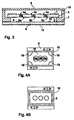
- Fig. 1 is an exploded perspective view of the dielectric filter and Fig. 3 is a cross-sectional view thereof taken in the longitudinal direction.
- reference numeral 3 denotes a dielectric plate made of dielectric ceramic having a linear expansion coefficient of for example 11 ppm/°C.
- An electrode 1 having non-electrode areas 4a, 4b, and 4c are formed on the upper surface of the dielectric plate 3.
- An electrode 2 are disposed on the lower surface of the dielectric plate 3 wherein non-electrode areas 5a, 5b, and 5c which are equal in shape to the non-electrode areas 4a, 4b, and 4c are formed in the electrode 2 at locations corresponding to the respective non-electrode areas 4a, 4b, and 4c.
- the regions 14a, 14b, 14c defined between the respective opposing non-electrode areas serve as TE010-mode dielectric resonators.
- the resonance frequencies of the dielectric resonators are set for example to 19 GHz.
- Reference numeral 15 denotes a case disposed such that the dielectric plate 1 is surrounded by the case 15 and the dielectric plate 1 is supported by the case 15.
- the case 15 is formed using an iron-based material such as S45C so as to have a linear expansion coefficient matched with that of the dielectric plate 3.
- the surface of the case 15 is plated with Ag or Au.
- Reference numeral 8 denotes a cover with which the upper side of the case 8 is covered. As with the case 15, the cover 8 is also made of an iron-based material and its surface is plated with Ag or Au.
- reference numeral 6 denotes a substrate.
- An electrode 12 is formed over the substantially entire area of the lower surface of the substrate 2.
- An electrode 11 is formed in a peripheral area of the upper surface of the substrate 6.
- microstrip lines 9 and 10 are formed on the upper surface of the substrate 6 wherein a part of each microstrip line serves as a probe (coupling member).
- a cavity is formed with the case 15, the cover 8, and the electrode 12 on the lower surface of the substrate 6.
- the substrate 6 In order to produce the substrate 6 at low cost and also to improve the productivity, it is preferable to employ, for example, a printed circuit substrate covered with copper foils designed for use in high-frequency applications.
- the linear expansion coefficient of the copper foils on the substrate is about 17 ppm/°C and thus there is a difference between the linear expansion coefficient of the copper foils and that of the case 15. Therefore, when the case and the substrate are soldered to each other for example at 200°C, the substrate (copper foils) 11 tries to contracts to a greater degree than the case 15 and thus a stress occurs.
- the case 15 is formed such that the supporting part for supporting the dielectric plate 3 and the side wall are formed in the integral fashion, the case 15 has a large total cross-sectional area and a large height.
- This structure allows the case 15 to have an extremely large strength against the bending stress compared to the conventional dielectric filter shown in Fig. 8. As a result, the case 15 is prevented from being warped. Therefore, when the dielectric plate 3 is mounted on the supporting part of the case 15, the stresses exerted on the four corners of the dielectric plate 3 are reduced to as low as one third those occurring in the conventional structure shown in Fig. 8.
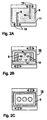
- Figs. 2A to 2C are plan views illustrating relative positional relationships among the substrate, the case, and the dielectric plate, wherein Fig. 2A is a plan view illustrating the substrate disposed separately from the other elements before being assembled. Fig. 2B is a plan view illustrating the substrate combined with the case, and Fig. 2C is a plan view illustrating the state where the dielectric plate is further combined.
- the electrode 11 and the microstrip lines 9 10 serving as probes are formed on the upper surface of the substrate 6.
- the substrate 6 has through-holes 13 formed near external leading portions of the microstrip lines 9 and 10 so that the upper electrode 11 and the lower electrode are electrically connected to each other via the through-holes 13.
- through-holes are also formed in areas where the substrate 11 is connected to the case 15. These through-holes prevent the microstrip lines 9 and 10 from being coupled with undesirable resonance occurring between the two electrodes formed on the upper and lower surfaces of the substrate 6.
- the substrate shown in Fig. 2A is bonded to the case 15 by soldering the case 15 to the upper surface of the substrate as shown in Fig. 2B.
- the dielectric plate 3 is then combined by bonding the lower surface of the dielectric plate 3 to the supporting part 16 of the case 15 via a conductive adhesive or the like as shown in Fig. 2C.
- the external size of the dielectric plate 3 is set to a value slightly smaller than the inner size of the side wall of the case 15 so that the side faces of the dielectric plate 3 does not come into tight contact with the side wall of the case 15.
- the dielectric plate 3 is supported by the case 15 in such a manner that only the peripheral area of the lower surface of the dielectric plate 3 is in contact with the case 15.
- the dielectric plate 3 In the conventional dielectric filter, although not shown in Fig. 8, after placing the dielectric plate 3 such that its peripheral part is sandwiched between the frame 7 and the cover 8, a ground plate is bonded to the side faces of the frame 7 and cover 8 so that they are grounded and so that the dielectric plate is electromagnetically shielded by the ground plate.
- the dielectric plate in the present invention, as can be seen from the above description with reference to the embodiment, the dielectric plate is disposed within the cavity and thus no ground plate is needed to be bonded. Therefore, it is possible to reduce the number of components and also the number of processing steps.
- the upper electrode 1 In the first embodiment, because no electrode is formed on the end faces of the dielectric plate 3, the upper electrode 1 is isolated from the ground.
- the return current does not flow across the side wall and thus it is not necessarily required that the electrodes formed on the upper and lower surfaces of the dielectric plate be DC connected.
- the isolation of the upper electrode 1 from the ground can cause a spurious problem.
- no significant degradation of characteristics in terms of the insertion loss and the attenuation characteristic is observed in actual evaluations. That is, the spurious is as low as required in practical applications.
- Figs. 4A and 4B illustrate a second embodiment of a dielectric filter according to the invention wherein Fig. 4A is a plan view illustrating a substrate 6 placed in a case 15 and Fig. 4B is a plan view illustrating the state in which a dielectric 3 is further combined.
- recesses 19 are formed in the four corners of the supporting part 16 of the case 15 such that the height of each corner becomes lower than the height of the other parts of the supporting part 16.
- the recesses allow the four corners of the dielectric plate 3 to be spaced slightly away from the supporting part 16 and thus the four corners of the dielectric plate 3 encounter a less stress due to the warp of the case 15.
- spaces 18a, 18b, and 18c formed at locations corresponding to the TE010-mode dielectric resonators.
- the sizes of these spaces 18a, 18b, and 18c are determined such that when these spaces are regarded as resonant spaces, the cut-off frequencies of the resonant spaces become higher than the resonance frequencies of the resonators formed in the dielectric plate and also such that the sizes of the spaces 18a, 18b, and 18c are greater than the outer sizes of the non-electrode areas formed on the dielectric plate, thereby suppressing undesired resonance modes in the space between the substrate 6 and the dielectric plate 3 and thus providing improved spurious characteristics.
- the spaces 18a, 18b, and 18c may be produced by means of cutting, etching, or other techniques at the same time as the recesses 19 are formed during the process of producing the case 15.
- Figs. 5A and 5B illustrate two examples of dielectric filters according to a third embodiment of the invention.
- Plan views of dielectric plates 3 placed in respective cases 15 are shown.
- the corners of the dielectric plate 3 are cut off in such a manner as to form so-called C-faces.
- the corners of the dielectric plate 3 are rounded in such a manner as to form R-corners.
- stresses in the four corners of the dielectric plate 3 placed in the case 15 are deconcentrated and thus cracks are prevented from occurring.
- Fig. 6 illustrates a duplexer according to a fourth embodiment of the invention wherein the state in which a substrate 6 is bonded to a case 15 and a dielectric plate 3 is further placed in the case 15 is shown in the form of a plan view.
- An electrode having five non-electrode areas 41a, 41b, 41c, 42a, and 42b are formed on the upper surface of the dielectric plate 3 and an electrode having non-electrode areas formed at locations opposing the non-electrode areas 41a, 41b, 41c, 42a, and 42b are disposed on the lower surface of the dielectric plate 3 thereby forming five TE010-mode dielectric resonators.
- dielectric resonators Of these dielectric resonators, three dielectric resonators formed at locations defined by the non-electrode areas 41a, 41, and 41c are used to form a 3-stage receiving filter. The remaining two resonators formed at locations defined by the non-electrode areas 42a and 42b are used to form a 2-stage transmitting filter.
- the case 15 has a lower partition wall projecting inward so as to provide isolation between the receiving filter and the transmitting filter.
- the upper side of the case 15 is covered with a cover similar to that shown in Fig. 1.
- the cover has an upper partition wall formed on its inner surface at a location opposing the lower partition wall such that the dielectric plate 3 is placed between the upper and lower partition walls.
- the dielectric resonators are surrounded by the electrode on the lower surface of the substrate 6, the case 15, the cover, and the upper and lower partition walls whereby the dielectric resonators are electromagnetically shielded and the transmitting and receiving filters are isolated from each other.
- microstrip lines 9r, 10r, 10t, and 9t serving as probes are formed on the substrate 6.
- the end portions of the microstrip lines 9r and 9t serve as a reception signal output port and a transmission signal input port, respectively.
- the end portions of the microstrip lines 10r and 10t are connected to each other via a dividing microstrip line which serves as an input/output port extending outward.
- the electrical length for each microstrip line 10r, 10t, between the equivalent short-circuited plane and the dividing point is determined so that the receiving filter has a high impedance at the transmitting frequency when seen from the dividing point and so that the transmitting filter also has a high impedance at the receiving frequency when seen from the dividing point.
- the invention can allows the case 15 to have high enough rigidity which prevents the dielectric plate 3 from having a crack. Thus, it is possible to realize a high-reliability duplexer.
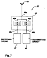
- Fig. 7 illustrates an embodiment of a communication device using the above-described duplexer as an antenna duplexer.
- reference numeral 46 denotes the antenna duplexer including receiving and transmitting filters 46a and 46b of the above-described type.
- a receiving circuit 47 is connected to the reception signal output port 46c of the antenna duplexer 46
- a transmitting circuit 48 is connected to the transmission signal input port 46d
- an antenna 49 is connected to the antenna port 46e so that they act, as a whole, as a communication device 50.
- This communication device may be employed for example in a high-frequency circuit of a portable telephone or the like.
- the receiving filter 46a and the transmitting filter 46b of the duplexer 46 may also be formed in a separate fashion similar to the dielectric filter shown in Fig. 1.
- the present invention has various advantages. That is, the case for supporting the dielectric plate and accommodating it has increased rigidity which prevents the case from being warped when the case is bonded to the substrate. Furthermore, because the dielectric plate is supported by the case in such a manner that only one surface of the dielectric plate is in contact with the case, the dielectric plate has a less stress due to the difference between the linear expansion coefficient of the dielectric plate and that of the case or the cover. As a result, the dielectric plate is prevented from encountering separation or a crack. Furthermore, it is possible to increase the rigidity of the case without having to increase the thickness of the side wall surrounding the side faces of the dielectric plate. This makes it possible to realize a dielectric filter with a reduced size.
- the supporting part of the case has recesses so that the corners of the dielectric plate are prevented from being in direct contact with the case. This allows the corners of the dielectric plate to have deconcentrated stresses and thus ensuring that the dielectric plate is prevented from encountering separation or cracks.
- the dielectric plate into a shape in which the corners of the dielectric plate are cut off or rounded, the stresses in the corners of the dielectric plate are deconcentrated and thus the dielectric plate is prevented in a more reliable fashion from encountering separation or cracks.
- the dielectric filter according to the invention may be used to form either one of or both of transmitting and receiving filters thereby realizing a small-sized duplexer in which the transmitting filter is disposed between the transmission signal input port and the input/output port, and the receiving filter is disposed between the reception signal output port and the input/output port.
Landscapes
- Physics & Mathematics (AREA)
- Electromagnetism (AREA)
- Control Of Motors That Do Not Use Commutators (AREA)
- Transceivers (AREA)
Applications Claiming Priority (2)
| Application Number | Priority Date | Filing Date | Title |
|---|---|---|---|
| JP9315998 | 1998-04-06 | ||
| JP10093159A JPH11289201A (ja) | 1998-04-06 | 1998-04-06 | 誘電体フィルタ、送受共用器および通信機 |
Publications (2)
| Publication Number | Publication Date |
|---|---|
| EP0949707A2 true EP0949707A2 (fr) | 1999-10-13 |
| EP0949707A3 EP0949707A3 (fr) | 2000-08-09 |
Family
ID=14074783
Family Applications (1)
| Application Number | Title | Priority Date | Filing Date |
|---|---|---|---|
| EP99106828A Withdrawn EP0949707A3 (fr) | 1998-04-06 | 1999-04-06 | Filtre diélectrique, duplexeur et dispositif de communication |
Country Status (6)
| Country | Link |
|---|---|
| US (1) | US6236291B1 (fr) |
| EP (1) | EP0949707A3 (fr) |
| JP (1) | JPH11289201A (fr) |
| KR (1) | KR100337166B1 (fr) |
| CN (1) | CN1144316C (fr) |
| TW (1) | TW418552B (fr) |
Cited By (3)
| Publication number | Priority date | Publication date | Assignee | Title |
|---|---|---|---|---|
| US6597260B2 (en) | 2000-09-06 | 2003-07-22 | Murata Manufacturing Co. Ltd. | Filter, multiplexer, and communication apparatus |
| GB2505138A (en) * | 2012-12-12 | 2014-02-19 | Radio Design Ltd | A Filter including resonating means and transmission line located on or associated with a support member located over at least a part of the filter body |
| CN105470618A (zh) * | 2015-12-25 | 2016-04-06 | 广东晖速通信技术股份有限公司 | 一种腔体谐振抑制结构 |
Families Citing this family (12)
| Publication number | Priority date | Publication date | Assignee | Title |
|---|---|---|---|---|
| US6937113B2 (en) * | 1998-06-09 | 2005-08-30 | Oki Electric Industry Co., Ltd. | Branching filter package |
| US6222426B1 (en) * | 1998-06-09 | 2001-04-24 | Oki Electric Industry, Co., Ltd. | Branching filter with a composite circuit of an LC circuit and a serial arm saw resonator |
| US6954124B2 (en) * | 2001-01-19 | 2005-10-11 | Matsushita Electric Industrial Co., Ltd. | High-frequency circuit device and high-frequency circuit module |
| JP3780417B2 (ja) * | 2002-02-12 | 2006-05-31 | 株式会社村田製作所 | 誘電体共振器、誘電体フィルタ、誘電体デュプレクサ、および通信装置 |
| DE10243670B3 (de) * | 2002-09-20 | 2004-02-12 | Eads Deutschland Gmbh | Hohlleiterfilter |
| CN1322629C (zh) * | 2003-11-13 | 2007-06-20 | 京瓷株式会社 | 电介质共振器、电介质滤波器以及无线通信设备 |
| KR100723865B1 (ko) | 2005-11-17 | 2007-05-31 | 한국전자통신연구원 | 집적화된 유전체 공진기 필터 및 이를 이용한 클럭 추출장치 |
| JP4519099B2 (ja) * | 2006-03-30 | 2010-08-04 | 三菱電機株式会社 | 高周波モジュール |
| JP6372413B2 (ja) * | 2014-07-07 | 2018-08-15 | 株式会社村田製作所 | フィルタ装置 |
| CN105514543B (zh) * | 2015-12-22 | 2018-02-23 | 华南理工大学 | 一种金属腔双工器 |
| GB2549276B (en) | 2016-04-11 | 2019-04-17 | Filtronic Broadband Ltd | A mm wave circuit |
| CN220785102U (zh) * | 2021-05-13 | 2024-04-16 | 株式会社村田制作所 | 层叠基板以及天线基板 |
Family Cites Families (8)
| Publication number | Priority date | Publication date | Assignee | Title |
|---|---|---|---|---|
| US5319329A (en) | 1992-08-21 | 1994-06-07 | Trw Inc. | Miniature, high performance MMIC compatible filter |
| US5446729A (en) * | 1993-11-01 | 1995-08-29 | Allen Telecom Group, Inc. | Compact, low-intermodulation multiplexer employing interdigital filters |
| JP2897678B2 (ja) | 1995-03-22 | 1999-05-31 | 株式会社村田製作所 | 誘電体共振器及び高周波帯域通過フィルタ装置 |
| JP2897117B2 (ja) * | 1995-09-19 | 1999-05-31 | 株式会社村田製作所 | 周波数可変型誘電体共振器 |
| JP3603453B2 (ja) * | 1996-03-12 | 2004-12-22 | 株式会社村田製作所 | 誘電体共振器および帯域通過フィルタ |
| JP3087664B2 (ja) * | 1996-11-06 | 2000-09-11 | 株式会社村田製作所 | 誘電体共振器装置及び高周波モジュール |
| EP0841714B1 (fr) * | 1996-11-06 | 2002-03-27 | Murata Manufacturing Co., Ltd. | Appareil à résonateur diélectrique et module à haute fréquence |
| JP3582350B2 (ja) * | 1997-04-21 | 2004-10-27 | 株式会社村田製作所 | 誘電体フィルタ、送受共用器および通信機 |
-
1998
- 1998-04-06 JP JP10093159A patent/JPH11289201A/ja active Pending
-
1999
- 1999-04-03 TW TW088105412A patent/TW418552B/zh not_active IP Right Cessation
- 1999-04-06 CN CNB99104861XA patent/CN1144316C/zh not_active Expired - Fee Related
- 1999-04-06 KR KR1019990011823A patent/KR100337166B1/ko not_active Expired - Fee Related
- 1999-04-06 EP EP99106828A patent/EP0949707A3/fr not_active Withdrawn
- 1999-04-06 US US09/286,518 patent/US6236291B1/en not_active Expired - Fee Related
Cited By (5)
| Publication number | Priority date | Publication date | Assignee | Title |
|---|---|---|---|---|
| US6597260B2 (en) | 2000-09-06 | 2003-07-22 | Murata Manufacturing Co. Ltd. | Filter, multiplexer, and communication apparatus |
| GB2505138A (en) * | 2012-12-12 | 2014-02-19 | Radio Design Ltd | A Filter including resonating means and transmission line located on or associated with a support member located over at least a part of the filter body |
| GB2505138B (en) * | 2012-12-12 | 2014-08-06 | Radio Design Ltd | Filter assembly and method of manufacture thereof |
| CN105470618A (zh) * | 2015-12-25 | 2016-04-06 | 广东晖速通信技术股份有限公司 | 一种腔体谐振抑制结构 |
| CN105470618B (zh) * | 2015-12-25 | 2019-03-12 | 广东晖速通信技术股份有限公司 | 一种腔体谐振抑制结构 |
Also Published As
| Publication number | Publication date |
|---|---|
| JPH11289201A (ja) | 1999-10-19 |
| EP0949707A3 (fr) | 2000-08-09 |
| CN1236196A (zh) | 1999-11-24 |
| KR19990082944A (ko) | 1999-11-25 |
| US6236291B1 (en) | 2001-05-22 |
| CN1144316C (zh) | 2004-03-31 |
| TW418552B (en) | 2001-01-11 |
| KR100337166B1 (ko) | 2002-05-18 |
Similar Documents
| Publication | Publication Date | Title |
|---|---|---|
| JP3344333B2 (ja) | フィルタ内蔵誘電体アンテナ、デュプレクサ内蔵誘電体アンテナおよび無線装置 | |
| US6236291B1 (en) | Dielectric filter, duplexer, and communication device | |
| EP1126541B1 (fr) | Filtre, duplexeur et dispositif de communication | |
| US6057745A (en) | Dielectric filter, transmitting/receiving duplexer, and communication apparatus having depressed parallel plate mode below a resonant frequency | |
| EP1148574B1 (fr) | Résonateur diélectrique, filtre, duplexeur et dispositif de communication | |
| JPH11186819A (ja) | 帯域阻止フィルタ及びデュプレクサ | |
| US5977848A (en) | Polar dielectric filter and dielectric duplexer incorporating same | |
| US6373352B1 (en) | Duplexer with stepped impedance resonators | |
| JPH11312903A (ja) | 誘電体フィルタ、誘電体デュプレクサ、通信機装置 | |
| EP1777774B1 (fr) | Dispositif diélectrique | |
| US6150906A (en) | HF filter using resonators having convex-concave structure | |
| CN1178331C (zh) | 介质谐振器、介质滤波器、介质双工器和通信装置 | |
| JP3464820B2 (ja) | 誘電体積層共振器および誘電体フィルタ | |
| JPH03124102A (ja) | 誘電体フィルタ | |
| US6573809B1 (en) | Dielectric resonator device, dielectric duplexer, and communication apparatus incorporating same | |
| JP2568149B2 (ja) | 誘電体フィルタ及び誘電体分波器 | |
| US20030151475A1 (en) | Dielectric resonator device, dielectric filter, dielectric duplexer, and communication apparatus | |
| JP2762332B2 (ja) | 積層型誘電体デュプレクサ | |
| JPH05191103A (ja) | 積層型誘電体フィルタ | |
| JP2002280806A (ja) | デュアルモード・バンドパスフィルタ及びデュアルモード・バンドパスフィルタの特性調整方法並びにデュプレクサ及び無線通信装置 | |
| JP2000357902A (ja) | 平面フィルタおよびそれを用いたデュプレクサおよびそれらを用いた高周波モジュールおよびそれを用いた通信装置 | |
| CN121748742A (zh) | 分布式元件射频滤波器 | |
| JPH04103201A (ja) | 誘電体帯域阻止フィルタ | |
| JP2003273605A (ja) | 導波管型フィルタ | |
| JP2000299601A (ja) | 誘電体デバイス及びその製造方法 |
Legal Events
| Date | Code | Title | Description |
|---|---|---|---|
| PUAI | Public reference made under article 153(3) epc to a published international application that has entered the european phase |
Free format text: ORIGINAL CODE: 0009012 |
|
| 17P | Request for examination filed |
Effective date: 19990406 |
|
| AK | Designated contracting states |
Kind code of ref document: A2 Designated state(s): DE FI GB SE |
|
| AX | Request for extension of the european patent |
Free format text: AL;LT;LV;MK;RO;SI |
|
| PUAL | Search report despatched |
Free format text: ORIGINAL CODE: 0009013 |
|
| AK | Designated contracting states |
Kind code of ref document: A3 Designated state(s): AT BE CH CY DE DK ES FI FR GB GR IE IT LI LU MC NL PT SE |
|
| AX | Request for extension of the european patent |
Free format text: AL;LT;LV;MK;RO;SI |
|
| AKX | Designation fees paid |
Free format text: DE FI GB SE |
|
| 17Q | First examination report despatched |
Effective date: 20050211 |
|
| STAA | Information on the status of an ep patent application or granted ep patent |
Free format text: STATUS: THE APPLICATION HAS BEEN WITHDRAWN |
|
| 18W | Application withdrawn |
Effective date: 20050729 |