EP0949714A2 - Board to board interconnect - Google Patents
Board to board interconnect Download PDFInfo
- Publication number
- EP0949714A2 EP0949714A2 EP99302753A EP99302753A EP0949714A2 EP 0949714 A2 EP0949714 A2 EP 0949714A2 EP 99302753 A EP99302753 A EP 99302753A EP 99302753 A EP99302753 A EP 99302753A EP 0949714 A2 EP0949714 A2 EP 0949714A2
- Authority
- EP
- European Patent Office
- Prior art keywords
- substrate
- printed circuit
- board
- disposed
- socket
- Prior art date
- Legal status (The legal status is an assumption and is not a legal conclusion. Google has not performed a legal analysis and makes no representation as to the accuracy of the status listed.)
- Granted
Links
Images

Classifications
-
- H—ELECTRICITY
- H05—ELECTRIC TECHNIQUES NOT OTHERWISE PROVIDED FOR
- H05K—PRINTED CIRCUITS; CASINGS OR CONSTRUCTIONAL DETAILS OF ELECTRIC APPARATUS; MANUFACTURE OF ASSEMBLAGES OF ELECTRICAL COMPONENTS
- H05K3/00—Apparatus or processes for manufacturing printed circuits
- H05K3/36—Assembling printed circuits with other printed circuits
- H05K3/368—Assembling printed circuits with other printed circuits parallel to each other
-
- H—ELECTRICITY
- H01—ELECTRIC ELEMENTS
- H01R—ELECTRICALLY-CONDUCTIVE CONNECTIONS; STRUCTURAL ASSOCIATIONS OF A PLURALITY OF MUTUALLY-INSULATED ELECTRICAL CONNECTING ELEMENTS; COUPLING DEVICES; CURRENT COLLECTORS
- H01R12/00—Structural associations of a plurality of mutually-insulated electrical connecting elements, specially adapted for printed circuits, e.g. printed circuit boards [PCB], flat or ribbon cables, or like generally planar structures, e.g. terminal strips, terminal blocks; Coupling devices specially adapted for printed circuits, flat or ribbon cables, or like generally planar structures; Terminals specially adapted for contact with, or insertion into, printed circuits, flat or ribbon cables, or like generally planar structures
- H01R12/50—Fixed connections
- H01R12/51—Fixed connections for rigid printed circuits or like structures
- H01R12/52—Fixed connections for rigid printed circuits or like structures connecting to other rigid printed circuits or like structures
- H01R12/523—Fixed connections for rigid printed circuits or like structures connecting to other rigid printed circuits or like structures by an interconnection through aligned holes in the boards or multilayer board
-
- H—ELECTRICITY
- H05—ELECTRIC TECHNIQUES NOT OTHERWISE PROVIDED FOR
- H05K—PRINTED CIRCUITS; CASINGS OR CONSTRUCTIONAL DETAILS OF ELECTRIC APPARATUS; MANUFACTURE OF ASSEMBLAGES OF ELECTRICAL COMPONENTS
- H05K2201/00—Indexing scheme relating to printed circuits covered by H05K1/00
- H05K2201/10—Details of components or other objects attached to or integrated in a printed circuit board
- H05K2201/10227—Other objects, e.g. metallic pieces
- H05K2201/10378—Interposers
-
- H—ELECTRICITY
- H05—ELECTRIC TECHNIQUES NOT OTHERWISE PROVIDED FOR
- H05K—PRINTED CIRCUITS; CASINGS OR CONSTRUCTIONAL DETAILS OF ELECTRIC APPARATUS; MANUFACTURE OF ASSEMBLAGES OF ELECTRICAL COMPONENTS
- H05K3/00—Apparatus or processes for manufacturing printed circuits
- H05K3/30—Assembling printed circuits with electric components, e.g. with resistors
- H05K3/32—Assembling printed circuits with electric components, e.g. with resistors electrically connecting electric components or wires to printed circuits
- H05K3/325—Assembling printed circuits with electric components, e.g. with resistors electrically connecting electric components or wires to printed circuits by abutting or pinching; Mechanical auxiliary parts therefor
Definitions
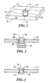
- Figs. 1 and 2 illustrate a resilient metalized particle interconnect 10 for establishing an electrical pathway from a first side 12 of a substrate 14 to a second side 16 of the substrate through an opening such as a via or hole 17.
- the resilient interconnect 10 includes a first cap member 18 disposed against the first side 12 of the substrate, a second cap member 20 disposed against the second side 16 of the substrate, and an intermediate stem member 22 disposed within the hole 17.
- the cap members may be formed as homogeneous metalized particle interconnects in accordance with techniques known in the art. In the illustrated example the cap members are a truncated cone shape.
- a cylindrical stem member 22 may be disposed between the first cap member 18 and the second cap member 20.
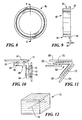
- a resilient interconnect 28 is formed by abutting first and second resilient conductive cap members 30, 32 on opposing sides of a resilient non-conducting stem member 34.
- the stem member 34 can be formed with a non-conducting resilient material such as a thermoplastic elastomer and the cap members 30, 32 may be formed with a resilient conductive material formed by combining a thermoplastic elastomer with particles of conductive material as described above.
- the alternative embodiment is formed by first disposing the stem member 34 in the hole or via 17 and then abutting the cap members 30, 32 against the non-conductive stem member 34.
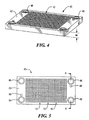
- board-to-board interconnect sockets may be employed to interconnect first and second non-parallel printed circuit boards 59, 61.
- a first substrate member 62 is joined with a second substrate member 64 at a desired angle such as 90 degrees or 45 degrees.
- Plated through-holes 66 are formed in the substrate and selectively interconnected by means such as conductive traces 68.
- Resilient interconnects 70 with one stem member and either one or two cap members are disposed in the through-holes and the first and second printed circuit boards 59, 61 are secured to the first and second substrate members 62, 64, respectively.
Landscapes
- Engineering & Computer Science (AREA)
- Manufacturing & Machinery (AREA)
- Microelectronics & Electronic Packaging (AREA)
- Coupling Device And Connection With Printed Circuit (AREA)
- Combinations Of Printed Boards (AREA)
- Multi-Conductor Connections (AREA)
Abstract
Description
Claims (15)
- An interconnection socket for providing an electrical connection from at least one contact on a first surface of a first printed circuit board to at least one contact on a first surface of a second printed circuit board, comprising:an electrically insulative substrate having a first surface and a second surface that define a predetermined thickness dimension; andan array of interconnect pathways, each comprising:a hole of predetermined cross-sectional shape and area formed through said substrate between said first surface and said second surface; anda resilient interconnect having first and second cap members over opposite ends of said hole.
- The interconnection socket of claim 1 wherein an electrically conductive stem member is disposed between the first and second cap members, thereby defining an electrically conductive column.
- The interconnection socket of claim 1 wherein an electrically insulative stem member is disposed between the first and second conductive cap members.
- The interconnection socket of claim 1 wherein said hole is lined with an electrically conductive material.
- The interconnection socket of claim 4 wherein said electrically conductive material is conductive plating.
- The interconnection socket of claim 4 wherein said electrically conductive material is carbon paste.
- The interconnection socket of claim 1 including an alignment post disposed in said substrate perpendicular to said first and second surfaces to facilitate alignment with at least one of the first and second printed circuit boards by fitting in a hole formed therein.
- The interconnection socket of claim 1 including an anti-overstress spacer that limits the proximity of the first printed circuit board relative to the first surface of said substrate.
- The interconnection socket of claim 8 wherein the anti-overstress spacer includes a rigid ring with a flange member that is disposed in an opening in the substrate and a shim member that is disposed on the first surface of the substrate.
- The interconnection socket of claim 9 wherein the flange member has a height dimension that is less than the height of the undeflected first cap member of the resilient interconnect that extends from the first surface of the substrate.
- The interconnection socket of claim 1 wherein said substrate includes a first substrate member joined with a second substrate member at a desired angle.
- The interconnection socket of claim 1 wherein said substrate includes six substrate surfaces joined in a cube shape.
- An interconnection socket for providing an electrical connection from at least one contact on a first surface of a first printed circuit board to at least one contact on a first surface of a second printed circuit board, comprising:a substrate having a first surface and a second surface that define a predetermined thickness dimension;a plurality of holes of predetermined diameter formed through said substrate between said first surface and said second surface;a resilient interconnect having first and second cap members disposed at opposite ends of at least some of said holes having an electrically conductive lining and a first cross-sectional area dimension;an alignment post disposed in said substrate perpendicular to said first and second surfaces to facilitate alignment with at least one of the first and second printed circuit boards by fitting in a hole formed therein; andan anti-overstress spacer that limits the proximity of the first printed circuit board relative to the first surface of said substrate.
- The interconnection socket of claim 13 wherein the anti-overstress spacer includes a rigid ring with a flange member that is disposed in an opening in the substrate and a shim member that is disposed on the first surface of the substrate.
- The interconnection socket of claim 13 wherein the flange member has a height dimension that is less than the height of the undeflected first cap member of the resilient interconnect that extends from, the first surface of the substrate.
Applications Claiming Priority (2)
| Application Number | Priority Date | Filing Date | Title |
|---|---|---|---|
| US56972 | 1998-04-08 | ||
| US09/056,972 US6056557A (en) | 1998-04-08 | 1998-04-08 | Board to board interconnect |
Publications (3)
| Publication Number | Publication Date |
|---|---|
| EP0949714A2 true EP0949714A2 (en) | 1999-10-13 |
| EP0949714A3 EP0949714A3 (en) | 2000-11-02 |
| EP0949714B1 EP0949714B1 (en) | 2003-12-03 |
Family
ID=22007715
Family Applications (1)
| Application Number | Title | Priority Date | Filing Date |
|---|---|---|---|
| EP99302753A Expired - Lifetime EP0949714B1 (en) | 1998-04-08 | 1999-04-08 | Board to board interconnect |
Country Status (5)
| Country | Link |
|---|---|
| US (1) | US6056557A (en) |
| EP (1) | EP0949714B1 (en) |
| JP (1) | JP2000003742A (en) |
| CA (1) | CA2268294C (en) |
| DE (1) | DE69913231T2 (en) |
Families Citing this family (24)
| Publication number | Priority date | Publication date | Assignee | Title |
|---|---|---|---|---|
| US6348659B1 (en) * | 1999-01-07 | 2002-02-19 | Thomas & Betts International, Inc. | Resilient electrical interconnects having non-uniform cross-section |
| IL128997A (en) * | 1999-03-15 | 2002-12-01 | Aprion Digital Ltd | Electrical connecting device |
| EP1061608A3 (en) * | 1999-05-10 | 2002-10-02 | Hirose Electric Co., Ltd. | Board to board electrical connectors |
| US6413102B2 (en) * | 1999-12-22 | 2002-07-02 | Micron Technology, Inc. | Center bond flip chip semiconductor carrier and a method of making and using it |
| US6471525B1 (en) * | 2000-08-24 | 2002-10-29 | High Connection Density, Inc. | Shielded carrier for land grid array connectors and a process for fabricating same |
| AU2002222447A1 (en) | 2000-12-05 | 2002-06-18 | Aprion Digital Ltd. | Board integrated resilient contact elements array and method of fabrication |
| US6790057B2 (en) | 2002-12-10 | 2004-09-14 | Tyco Electronics Corporation | Conductive elastomeric contact system with anti-overstress columns |
| US6796810B2 (en) | 2002-12-10 | 2004-09-28 | Tyco Electronics Corporation | Conductive elastomeric contact system |
| DE10324047B4 (en) * | 2003-05-27 | 2013-02-28 | Continental Automotive Gmbh | Electronic unit and method for manufacturing an electronic unit |
| US20050082160A1 (en) * | 2003-10-15 | 2005-04-21 | Sharper Image Corporation | Electro-kinetic air transporter and conditioner devices with a mesh collector electrode |
| TWI343156B (en) * | 2003-10-16 | 2011-06-01 | Tyco Electronics Corp | Conductive elastomeric contact system with anti-overstress columns |
| US7059867B1 (en) * | 2005-03-30 | 2006-06-13 | Artesyn Technologies, Inc. | High density multi-lead surface mount interconnect and devices including same |
| US7070420B1 (en) | 2005-08-08 | 2006-07-04 | Wakefield Steven B | Electrical interconnect system utilizing nonconductive elastomeric elements and continuous conductive elements |
| US7549870B2 (en) * | 2007-01-03 | 2009-06-23 | Tyco Electronics Corporation | Electrical interconnect device utilizing contact caps |
| US7572131B2 (en) * | 2007-03-13 | 2009-08-11 | Tyco Electronics Corporation | Electrical interconnect system utilizing non-conductive elastomeric elements |
| US7726976B2 (en) * | 2007-11-09 | 2010-06-01 | Tyco Electronics Corporation | Shielded electrical interconnect |
| CN101982903A (en) * | 2010-09-15 | 2011-03-02 | 华为技术有限公司 | Circuit board connector and communication equipment |
| WO2013089687A1 (en) * | 2011-12-13 | 2013-06-20 | Empire Technology Development Llc | Elastomer adhesions |
| US9876298B2 (en) | 2014-08-04 | 2018-01-23 | Te Connectivity Corporation | Flexible connector and methods of manufacture |
| US10135190B2 (en) | 2014-08-04 | 2018-11-20 | Vaios Nikolaos Bozikis | Electrical plug and socket securement system |
| US10141690B2 (en) | 2014-08-04 | 2018-11-27 | Vaios Nikolaos Bozikis | Electrical plug and socket securement system |
| US10104772B2 (en) | 2014-08-19 | 2018-10-16 | International Business Machines Incorporated | Metallized particle interconnect with solder components |
| US10320122B2 (en) | 2017-02-25 | 2019-06-11 | Vaios Nikolaos Bozikis | Double side adjustable electrical cord securement device |
| WO2021212434A1 (en) * | 2020-04-23 | 2021-10-28 | 宏启胜精密电子(秦皇岛)有限公司 | Plate-to-plate connection structure and fabrication method therefor |
Family Cites Families (10)
| Publication number | Priority date | Publication date | Assignee | Title |
|---|---|---|---|---|
| JPS61145888A (en) * | 1984-12-20 | 1986-07-03 | 松下電器産業株式会社 | Printed wiring board connector |
| US5098305A (en) * | 1987-05-21 | 1992-03-24 | Cray Research, Inc. | Memory metal electrical connector |
| JPH02139987A (en) * | 1988-11-18 | 1990-05-29 | Fujitsu Ltd | Common wiring mechanism for a plurality of printed boards |
| WO1993013637A1 (en) * | 1991-12-31 | 1993-07-08 | Tessera, Inc. | Multi-layer circuit construction methods and structures with customization features and components for use therein |
| JP2534003B2 (en) * | 1992-03-17 | 1996-09-11 | 信越化学工業株式会社 | Laminated rubber molding |
| US5417577A (en) * | 1992-09-23 | 1995-05-23 | At&T Corp. | Interconnection method and apparatus |
| JPH0778645A (en) * | 1993-09-09 | 1995-03-20 | Japan Aviation Electron Ind Ltd | Connector for electrical connection |
| US5599193A (en) * | 1994-08-23 | 1997-02-04 | Augat Inc. | Resilient electrical interconnect |
| WO1997013295A1 (en) * | 1995-10-06 | 1997-04-10 | The Whitaker Corporation | Connector and manufacturing method therefor |
| JP2987101B2 (en) * | 1996-04-15 | 1999-12-06 | 株式会社ニッシン | Method for connecting semiconductor device and connector for semiconductor device |
-
1998
- 1998-04-08 US US09/056,972 patent/US6056557A/en not_active Expired - Lifetime
-
1999
- 1999-04-07 CA CA002268294A patent/CA2268294C/en not_active Expired - Fee Related
- 1999-04-08 JP JP11101298A patent/JP2000003742A/en active Pending
- 1999-04-08 EP EP99302753A patent/EP0949714B1/en not_active Expired - Lifetime
- 1999-04-08 DE DE69913231T patent/DE69913231T2/en not_active Expired - Lifetime
Also Published As
| Publication number | Publication date |
|---|---|
| JP2000003742A (en) | 2000-01-07 |
| CA2268294C (en) | 2002-06-11 |
| US6056557A (en) | 2000-05-02 |
| EP0949714A3 (en) | 2000-11-02 |
| CA2268294A1 (en) | 1999-10-08 |
| DE69913231D1 (en) | 2004-01-15 |
| EP0949714B1 (en) | 2003-12-03 |
| DE69913231T2 (en) | 2004-09-09 |
Similar Documents
| Publication | Publication Date | Title |
|---|---|---|
| US6056557A (en) | Board to board interconnect | |
| US7331796B2 (en) | Land grid array (LGA) interposer utilizing metal-on-elastomer hemi-torus and other multiple points of contact geometries | |
| US6796810B2 (en) | Conductive elastomeric contact system | |
| CN101299492B (en) | Electrical interconnect system utilizing non-conductive elastomeric elements | |
| EP0437606A1 (en) | ELECTRIC CONNECTORS. | |
| CN102735883A (en) | Electrical interconnect device | |
| US12171064B2 (en) | Interconnect and method for manufacturing the same | |
| US7466154B2 (en) | Conductive particle filled polymer electrical contact | |
| JPH0778645A (en) | Connector for electrical connection |
Legal Events
| Date | Code | Title | Description |
|---|---|---|---|
| PUAI | Public reference made under article 153(3) epc to a published international application that has entered the european phase |
Free format text: ORIGINAL CODE: 0009012 |
|
| AK | Designated contracting states |
Kind code of ref document: A2 Designated state(s): DE ES FR GB IT |
|
| AX | Request for extension of the european patent |
Free format text: AL;LT;LV;MK;RO;SI |
|
| PUAL | Search report despatched |
Free format text: ORIGINAL CODE: 0009013 |
|
| AK | Designated contracting states |
Kind code of ref document: A3 Designated state(s): AT BE CH CY DE DK ES FI FR GB GR IE IT LI LU MC NL PT SE |
|
| AX | Request for extension of the european patent |
Free format text: AL;LT;LV;MK;RO;SI |
|
| 17P | Request for examination filed |
Effective date: 20010424 |
|
| AKX | Designation fees paid |
Free format text: DE ES FR GB IT |
|
| RAP1 | Party data changed (applicant data changed or rights of an application transferred) |
Owner name: THOMAS & BETTS INTERNATIONAL, INC. |
|
| 17Q | First examination report despatched |
Effective date: 20021203 |
|
| GRAH | Despatch of communication of intention to grant a patent |
Free format text: ORIGINAL CODE: EPIDOS IGRA |
|
| RIC1 | Information provided on ipc code assigned before grant |
Ipc: 7H 01R 13/03 B Ipc: 7H 01R 12/16 B Ipc: 7H 01R 12/06 A |
|
| RIC1 | Information provided on ipc code assigned before grant |
Ipc: 7H 01R 13/03 B Ipc: 7H 01R 12/16 B Ipc: 7H 01R 12/06 A |
|
| GRAS | Grant fee paid |
Free format text: ORIGINAL CODE: EPIDOSNIGR3 |
|
| GRAA | (expected) grant |
Free format text: ORIGINAL CODE: 0009210 |
|
| RIN1 | Information on inventor provided before grant (corrected) |
Inventor name: DELPRETE, STEPHEN D. Inventor name: CROTZER, DAVID R. |
|
| AK | Designated contracting states |
Kind code of ref document: B1 Designated state(s): DE ES FR GB IT |
|
| PG25 | Lapsed in a contracting state [announced via postgrant information from national office to epo] |
Ref country code: IT Free format text: LAPSE BECAUSE OF FAILURE TO SUBMIT A TRANSLATION OF THE DESCRIPTION OR TO PAY THE FEE WITHIN THE PRESCRIBED TIME-LIMIT;WARNING: LAPSES OF ITALIAN PATENTS WITH EFFECTIVE DATE BEFORE 2007 MAY HAVE OCCURRED AT ANY TIME BEFORE 2007. THE CORRECT EFFECTIVE DATE MAY BE DIFFERENT FROM THE ONE RECORDED. Effective date: 20031203 |
|
| REG | Reference to a national code |
Ref country code: GB Ref legal event code: FG4D |
|
| REF | Corresponds to: |
Ref document number: 69913231 Country of ref document: DE Date of ref document: 20040115 Kind code of ref document: P |
|
| PG25 | Lapsed in a contracting state [announced via postgrant information from national office to epo] |
Ref country code: ES Free format text: LAPSE BECAUSE OF FAILURE TO SUBMIT A TRANSLATION OF THE DESCRIPTION OR TO PAY THE FEE WITHIN THE PRESCRIBED TIME-LIMIT Effective date: 20040314 |
|
| ET | Fr: translation filed | ||
| PLBE | No opposition filed within time limit |
Free format text: ORIGINAL CODE: 0009261 |
|
| STAA | Information on the status of an ep patent application or granted ep patent |
Free format text: STATUS: NO OPPOSITION FILED WITHIN TIME LIMIT |
|
| 26N | No opposition filed |
Effective date: 20040906 |
|
| PGFP | Annual fee paid to national office [announced via postgrant information from national office to epo] |
Ref country code: GB Payment date: 20130429 Year of fee payment: 15 Ref country code: DE Payment date: 20130429 Year of fee payment: 15 |
|
| PGFP | Annual fee paid to national office [announced via postgrant information from national office to epo] |
Ref country code: FR Payment date: 20130506 Year of fee payment: 15 |
|
| REG | Reference to a national code |
Ref country code: DE Ref legal event code: R119 Ref document number: 69913231 Country of ref document: DE |
|
| GBPC | Gb: european patent ceased through non-payment of renewal fee |
Effective date: 20140408 |
|
| REG | Reference to a national code |
Ref country code: FR Ref legal event code: ST Effective date: 20141231 |
|
| REG | Reference to a national code |
Ref country code: DE Ref legal event code: R079 Ref document number: 69913231 Country of ref document: DE Free format text: PREVIOUS MAIN CLASS: H01R0012060000 Ipc: H01R0012500000 |
|
| PG25 | Lapsed in a contracting state [announced via postgrant information from national office to epo] |
Ref country code: DE Free format text: LAPSE BECAUSE OF NON-PAYMENT OF DUE FEES Effective date: 20141101 Ref country code: GB Free format text: LAPSE BECAUSE OF NON-PAYMENT OF DUE FEES Effective date: 20140408 |
|
| PG25 | Lapsed in a contracting state [announced via postgrant information from national office to epo] |
Ref country code: FR Free format text: LAPSE BECAUSE OF NON-PAYMENT OF DUE FEES Effective date: 20140430 |
|
| REG | Reference to a national code |
Ref country code: DE Ref legal event code: R119 Ref document number: 69913231 Country of ref document: DE Effective date: 20141101 Ref country code: DE Ref legal event code: R079 Ref document number: 69913231 Country of ref document: DE Free format text: PREVIOUS MAIN CLASS: H01R0012060000 Ipc: H01R0012500000 Effective date: 20150127 |