EP0950924B1 - Appareil de projection lithographique et méthode de fabrication d'un dispositif - Google Patents
Appareil de projection lithographique et méthode de fabrication d'un dispositif Download PDFInfo
- Publication number
- EP0950924B1 EP0950924B1 EP19990302740 EP99302740A EP0950924B1 EP 0950924 B1 EP0950924 B1 EP 0950924B1 EP 19990302740 EP19990302740 EP 19990302740 EP 99302740 A EP99302740 A EP 99302740A EP 0950924 B1 EP0950924 B1 EP 0950924B1
- Authority
- EP
- European Patent Office
- Prior art keywords
- projection
- mask
- radiation
- projection apparatus
- radiation source
- Prior art date
- Legal status (The legal status is an assumption and is not a legal conclusion. Google has not performed a legal analysis and makes no representation as to the accuracy of the status listed.)
- Expired - Lifetime
Links
- 238000004519 manufacturing process Methods 0.000 title claims description 11
- 230000005855 radiation Effects 0.000 claims description 38
- 230000000873 masking effect Effects 0.000 claims description 37
- 238000005286 illumination Methods 0.000 claims description 31
- 239000000758 substrate Substances 0.000 claims description 29
- 239000000463 material Substances 0.000 claims description 8
- 230000003287 optical effect Effects 0.000 claims description 7
- 238000000576 coating method Methods 0.000 claims description 5
- 239000011248 coating agent Substances 0.000 claims description 4
- 238000003384 imaging method Methods 0.000 claims description 4
- 238000012886 linear function Methods 0.000 claims description 4
- XAGFODPZIPBFFR-UHFFFAOYSA-N aluminium Chemical compound [Al] XAGFODPZIPBFFR-UHFFFAOYSA-N 0.000 claims description 2
- 229910052782 aluminium Inorganic materials 0.000 claims description 2
- 239000011521 glass Substances 0.000 claims description 2
- 239000010453 quartz Substances 0.000 claims description 2
- 238000007493 shaping process Methods 0.000 claims description 2
- VYPSYNLAJGMNEJ-UHFFFAOYSA-N silicon dioxide Inorganic materials O=[Si]=O VYPSYNLAJGMNEJ-UHFFFAOYSA-N 0.000 claims description 2
- 239000004411 aluminium Substances 0.000 claims 1
- 230000000903 blocking effect Effects 0.000 claims 1
- 238000000034 method Methods 0.000 description 12
- 230000006870 function Effects 0.000 description 7
- 230000008569 process Effects 0.000 description 5
- XUIMIQQOPSSXEZ-UHFFFAOYSA-N Silicon Chemical compound [Si] XUIMIQQOPSSXEZ-UHFFFAOYSA-N 0.000 description 1
- 239000006096 absorbing agent Substances 0.000 description 1
- 238000011217 control strategy Methods 0.000 description 1
- 238000001514 detection method Methods 0.000 description 1
- 238000011161 development Methods 0.000 description 1
- 238000010586 diagram Methods 0.000 description 1
- 230000000694 effects Effects 0.000 description 1
- 238000005530 etching Methods 0.000 description 1
- 230000004907 flux Effects 0.000 description 1
- 238000007689 inspection Methods 0.000 description 1
- 238000005468 ion implantation Methods 0.000 description 1
- 239000004973 liquid crystal related substance Substances 0.000 description 1
- 238000001459 lithography Methods 0.000 description 1
- 230000005381 magnetic domain Effects 0.000 description 1
- 238000005259 measurement Methods 0.000 description 1
- 230000015654 memory Effects 0.000 description 1
- QSHDDOUJBYECFT-UHFFFAOYSA-N mercury Chemical compound [Hg] QSHDDOUJBYECFT-UHFFFAOYSA-N 0.000 description 1
- 229910052753 mercury Inorganic materials 0.000 description 1
- 238000001465 metallisation Methods 0.000 description 1
- 238000012544 monitoring process Methods 0.000 description 1
- 230000003647 oxidation Effects 0.000 description 1
- 238000007254 oxidation reaction Methods 0.000 description 1
- 238000005498 polishing Methods 0.000 description 1
- 230000037452 priming Effects 0.000 description 1
- 238000012545 processing Methods 0.000 description 1
- 230000009467 reduction Effects 0.000 description 1
- 230000004044 response Effects 0.000 description 1
- 239000004065 semiconductor Substances 0.000 description 1
- 229910052710 silicon Inorganic materials 0.000 description 1
- 239000010703 silicon Substances 0.000 description 1
- 239000010409 thin film Substances 0.000 description 1
- 238000011144 upstream manufacturing Methods 0.000 description 1
Images
Classifications
-
- G—PHYSICS
- G03—PHOTOGRAPHY; CINEMATOGRAPHY; ANALOGOUS TECHNIQUES USING WAVES OTHER THAN OPTICAL WAVES; ELECTROGRAPHY; HOLOGRAPHY
- G03F—PHOTOMECHANICAL PRODUCTION OF TEXTURED OR PATTERNED SURFACES, e.g. FOR PRINTING, FOR PROCESSING OF SEMICONDUCTOR DEVICES; MATERIALS THEREFOR; ORIGINALS THEREFOR; APPARATUS SPECIALLY ADAPTED THEREFOR
- G03F7/00—Photomechanical, e.g. photolithographic, production of textured or patterned surfaces, e.g. printing surfaces; Materials therefor, e.g. comprising photoresists; Apparatus specially adapted therefor
- G03F7/70—Microphotolithographic exposure; Apparatus therefor
- G03F7/70483—Information management; Active and passive control; Testing; Wafer monitoring, e.g. pattern monitoring
- G03F7/7055—Exposure light control in all parts of the microlithographic apparatus, e.g. pulse length control or light interruption
- G03F7/70558—Dose control, i.e. achievement of a desired dose
-
- G—PHYSICS
- G03—PHOTOGRAPHY; CINEMATOGRAPHY; ANALOGOUS TECHNIQUES USING WAVES OTHER THAN OPTICAL WAVES; ELECTROGRAPHY; HOLOGRAPHY
- G03F—PHOTOMECHANICAL PRODUCTION OF TEXTURED OR PATTERNED SURFACES, e.g. FOR PRINTING, FOR PROCESSING OF SEMICONDUCTOR DEVICES; MATERIALS THEREFOR; ORIGINALS THEREFOR; APPARATUS SPECIALLY ADAPTED THEREFOR
- G03F7/00—Photomechanical, e.g. photolithographic, production of textured or patterned surfaces, e.g. printing surfaces; Materials therefor, e.g. comprising photoresists; Apparatus specially adapted therefor
- G03F7/70—Microphotolithographic exposure; Apparatus therefor
- G03F7/70058—Mask illumination systems
- G03F7/70066—Size and form of the illuminated area in the mask plane, e.g. reticle masking blades or blinds
-
- G—PHYSICS
- G03—PHOTOGRAPHY; CINEMATOGRAPHY; ANALOGOUS TECHNIQUES USING WAVES OTHER THAN OPTICAL WAVES; ELECTROGRAPHY; HOLOGRAPHY
- G03F—PHOTOMECHANICAL PRODUCTION OF TEXTURED OR PATTERNED SURFACES, e.g. FOR PRINTING, FOR PROCESSING OF SEMICONDUCTOR DEVICES; MATERIALS THEREFOR; ORIGINALS THEREFOR; APPARATUS SPECIALLY ADAPTED THEREFOR
- G03F7/00—Photomechanical, e.g. photolithographic, production of textured or patterned surfaces, e.g. printing surfaces; Materials therefor, e.g. comprising photoresists; Apparatus specially adapted therefor
- G03F7/70—Microphotolithographic exposure; Apparatus therefor
- G03F7/70216—Mask projection systems
- G03F7/70358—Scanning exposure, i.e. relative movement of patterned beam and workpiece during imaging
Definitions
- the present invention relates to dose control in lithographic projection apparatus comprising:
- the projection system may hereinafter be referred to as the "lens"; however, this term should be broadly interpreted as encompassing various types of projection system, including refractive optics, reflective optics and catadioptric systems, for example.
- the radiation system may also include elements operating according to any of these principles for directing, shaping or controlling the projection beam of radiation and such elements may also be referred to below, collectively or singularly, as a "lens".
- Any refractive, reflective or catadioptric elements in the radiation or illumination systems may be based on a substrate of glass or another suitable material, and may be provided with either single- or multi-layer coatings as desired.
- first and second object tables may be referred to as the "mask table” and the "substrate table”, respectively.
- the lithographic apparatus may be of a type having two or more mask tables and/or two or more substrate tables. In such "multiple stage” devices the additional tables may be used in parallel or preparatory steps may be carried out on one or more stages while one or more other stages are being used for exposures. Twin stage lithographic apparatus are described in International Patent Applications WO 98/28665 and WO 98/40791.
- Lithographic projection apparatus can be used, for example, in the manufacture of integrated circuits (ICs).
- the mask (reticle) may contain a circuit pattern corresponding to an individual layer of the IC, and this pattern can then be imaged onto a target area (die) on a substrate (silicon wafer) which has been coated with a layer of photosensitive material (resist).
- a single wafer will contain a whole network of adjacent dies which are successively irradiated through the reticle, one at a time.
- each die is irradiated by exposing the entire reticle pattern onto the die in one go; such an apparatus is commonly referred to as a wafer stepper.
- each die is irradiated by progressively scanning the reticle pattern under the projection beam in a given reference direction (the "scanning" direction) while synchronously scanning the wafer table parallel or anti-parallel to this direction; since, in general, the projection system will have a magnification factor M ⁇ 1, the speed v at which the wafer table is scanned will be a factor M times that at which the reticle table is scanned. More information with regard to lithographic devices as here described can be gleaned from International Patent Application WO 97/33205.
- a step-and-scan exposure apparatus is described in WO 97/33204.
- reticle masking blades are used to define a slit through which an illumination beam passes to illuminate a rectangular portion of a reticle, an image of which is projected onto a wafer with a magnification M.
- the reticle is moved so that the illuminated portion scans the whole pattern to be imaged.
- the wafer is moved synchronously at a speed M times that of the reticle in the opposite direction to the reticle so that the whole pattern is imaged onto the wafer.
- the wafer is stepped to the beginning of the next field to be illuminated, and the illumination process is repeated.
- a lithographic projection apparatus comprising:
- the present inventors have determined that exposure (dose) errors occur at the beginning and end of the scan and are caused by reflections from the reticle masking blades.
- the present invention therefore provides means for compensating for the increased illumination as the slit defined by the beam masking means (e.g. reticle masking blades) is opened and closed.
- the present invention enables the slit illumination to be controlled so as to be constant and uniform throughout the scan, thus improving the consistency and yield of an IC manufacturing process employing the inventive apparatus.
- said compensation means comprise radiation source control means adapted to control the output of the radiation source (e.g. lamp), which is employed to produce the illumination beam, in accordance with the degree of opening of the beam masking means, to compensate for said variation.
- the radiation source e.g. lamp
- said radiation source control means are adapted to control the radiation source output according to a function determined by the cross-section of the projection beam when the beam masking means are fully open and the size of the reticle pattern to be imaged. Said function may be calculated from empirically derived reference values.
- the present invention also encompasses a device manufacturing method according to claim 14.
- said compensating means may be such that the beam masking means are constructed of a material substantially transparent to said illumination beam and are shaped so that portions of said illumination beam incident thereon are totally internally reflected.
- a pattern in a mask is imaged onto a substrate which is at least partially covered by a layer of energy-sensitive material (resist).
- the substrate Prior to this imaging step, the substrate may undergo various procedures, such as priming, resist coating and a soft bake. After exposure, the substrate may be subjected to other procedures, such as a post-exposure bake (PEB), development, a hard bake and measurement/inspection of the imaged features.
- PEB post-exposure bake
- This array of procedures is used as a basis to pattern an individual layer of a device, e.g. an IC.
- Such a patterned layer of may then undergo various processes such as etching, ion-implantation (doping) metallisation, oxidation, chemo-mechanical polishing, etc., all intended to finish off an individual layer. If several layers are required, then the whole procedure, or a variant thereof, will have to be repeated for each new layer. Eventually, an array of devices will be present on the substrate (wafer). These devices are then separated from one another by a technique such as dicing or sawing, whence the individual devices can be mounted on a carrier, connected to pins, etc. Further information regarding such processes can be obtained, for example, from the book “Microchip Fabrication: A Practical Guide to Semiconductor Processing", Third Edition, by Peter van Zant, McGraw Hill Publishing Co., 1997, ISBN 0-07-067250-4.
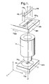
- FIG. 1 shows a demagnified image of the mask MA formed on the substrate W mounted on table WH in a step-and-scan apparatus; the magnification M of the projection lens system is, for example, 1/4.
- the projection beam PB is partially obstructed by reticle masking blades (not shown) so as to have, at the area of the mask, for example, a rectangular cross-section PB c so that a rectangular part MA B of this mask is illuminated.
- This part is imaged by the projection lens system PL on a similarly rectangular part W B of the substrate W.
- the entire mask is successively illuminated and the entire mask pattern is imaged on an area C of the substrate.
- the mask and the substrate may also be moved in the same X direction.
- the substrate holder After the mask pattern has been imaged on a first Integrated Circuit (IC) area (i.e. target area), the substrate holder is moved with respect to the mask along a distance which is equal to the period of the IC areas in the X direction or the Y direction, and the mask is imaged on a second IC area (i.e. target area) by the scanning radiation pattern PB c .
- IC Integrated Circuit
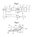
- an illumination system of a lithographic apparatus The relevant components of an illumination system of a lithographic apparatus according to the present invention are shown schematically in Figure 2.
- Light emitted by radiation source 1, e.g. a mercury lamp, is collected by elliptical mirror 2 and reflected into the first element 3a of the illumination optical system 3 which projects the light onto the reticle 8; the radiation source may also be a laser.
- a radiation source may emit UV light having a wavelength of 365nm, 248nm, 193nm or 157nm, for example.
- a shutter 4 is provided between the lamp 1 and the illumination optical system 3.
- a portion of the illumination light is diverted by a beam splitter 5 to energy sensor 6 to enable monitoring of the amount of optical energy reaching the reticle 8.
- the actual dimensions of the scanning radiation pattern are determined by reticle masking means 7 which define a slit through which the reticle is illuminated.
- the remaining components of the device are omitted for clarity but may be as illustrated in Figure 1.
- the reticle masking blades which comprise the reticle masking means 7, are closed.
- the leading blade in the scan direction moves to open the slit, the slit is then scanned over the field and at the end of the scan the following blade is moved to close the slit.
- the lamp intensity is reduced when the slit is closed and increased in synchronism with the opening of the slit.
- the system comprises a lamp control circuit 10 which controls the lamp power supply 9 so that the lamp intensity follows a reciprocal linear function of X to ensure that the radiation intensity at wafer level is constant.
- Data indicating the slit cross-section are provided to the lamp control circuit 10 by the reticle masking servo control 11.
- the illumination intensity variation as a function of X differs for different combinations of slit cross-section and die size and therefore needs to be adjusted for each manufacturing sequence.
- the function may be measured each time. Alternatively, it may be measured in advance for a plurality of slit and die combinations and the relevant function for a given manufacturing run modeled from these reference functions.
- the reticle masking blades are constructed to avoid reflecting the illumination light.
- the reticle masking blade 70 has a main body 71 constructed of quartz.
- the front face 70a of the blade 70, on which the illumination light L is incident, is flat.
- the rear face 70b has an inclined portion 70c so that the blade is thinnest at its edge 70d.
- the angle ⁇ of the inclined face 70c is set such that the illumination light incident on the front face 70a is totally internally reflected and directed sideways, out of the illumination beam, to an absorber.
- the front face 70a may be coated with an anti-reflection coating optimized for the illumination light frequency.
- the rear face of the blade 70 may be coated with a reflective metallic layer 72 (e.g. comprised of aluminum).
- a reflective metallic layer 72 e.g. comprised of aluminum.
- Reflections from the reticle masking blades are thereby eliminated and the intensity density of the illumination light is made constant throughout the opening of the blades.
- An alternative method proposed by the invention to compensate for the increase in intensity density of the illumination light is to control the scan speed.
- the intensity density is a linear function of X. This can be compensated for by a linearly increasing scan speed. Since the scan speed is proportional to the slit cross-section and illumination intensity, but inversely proportional to the dose, it can be seen that the dose will be constant as a function of X.
- the reticle table and reticle masking blades must be controlled to move correspondingly with the scan speed defined above.
- the energy sensor 6 is positioned downstream of the shutter 4 because it is desired to place it as close to the reticle as possible to take account of the effect of as much of the illumination optical system as possible.
- This closed loop feedback control is advantageous when the shutter is open. However, when the shutter is closed no light reaches the sensor and it is therefore not possible to control the lamp on the basis of this sensor.
- the present invention therefore provides an additional control system for use when the shutter is closed.
- This additional control loop may comprise a current control loop which provides open loop control of the lamp brightness through closed loop control of the current flowing through it.
- an additional lamp sensor 12 is provided upstream of the shutter to detect the brightness of the lamp directly. A signal from the lamp sensor is fed to the lamp control circuit 10 which stabilizes the light flux.
- the shutter 4 is fully opened and the light sensor 6 and lamp 1 allowed to settle to the appropriate level under control of the light sensor 6 before the reticle masking blades 7 are opened and the scan begins.
- This method is very reliable but has a potential disadvantage in that throughput will be reduced if the lamp settling time is longer than the substrate table settling time.
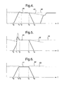
- This control process is illustrated in Figure 4.
- the shutter opens and the energy detected by the light sensor 6, shown by solid line 41, rises to the level of the actual lamp output, shown by dashed line 42.
- the measured energy equals the actual lamp energy.
- the sensor is allowed to settle and the lamp output adjusted to the desired level, shown by dotted line 43.
- the exposure begins at t 2 and ends at t 3 during which time the lamp output is controlled on the basis of the lamp sensor 6.
- the lamp sensor signal falls off as the shutter closes until it reaches zero at t 4 when the shutter is fully closed.
- An alternative control strategy makes use of the known properties of the lamp control system and the known shutter opening time, e.g. 10 ms. This process is illustrated in Figure 5. If control is switched to the light sensor 6 at time t 1 , perhaps halfway through the shutter opening, the light sensor control will cause a large overshoot in the lamp power because the light sensor is only sensing half of its output. Because the light sensor control loop has a very fast response time, the lamp power will be brought quickly to the correct level by the time the exposure begins at t 2 . Proper selection of the timing of changeover of control will ensure that the lamp is at the correct level most rapidly.
- the third alternative is to operate both control loops simultaneously with the lamp power being controlled on the basis of the lower of the two controls and the set point for the shutter closed (i.e. lamp sensor) control loop set slightly higher than the desired energy level.
- This is shown in Figure 6.
- the light sensor 6 control loop will command a very high lamp output so that control will follow the shutter closed control loop.
- the output level commanded by light sensor 6 will fall until t 1 when it drops below the shutter closed set point and the light sensor control takes over.
- the lamp output will fall quickly to the desired level and exposure can begin at t 2 .
- the lamp output will rise as the light sensor 6 commands an increase in output to compensate for the reduction in light reaching it. Very soon however, the output commanded by the light sensor 6 will rise above the shutter closed set point and that control will therefore takeover. In this way switching between control loops is automatic.
Landscapes
- Physics & Mathematics (AREA)
- General Physics & Mathematics (AREA)
- Exposure And Positioning Against Photoresist Photosensitive Materials (AREA)
- Exposure Of Semiconductors, Excluding Electron Or Ion Beam Exposure (AREA)
Claims (14)
- Appareil de projection lithographique comportant :un système de rayonnement (2, 3) pour fournir un faisceau de projection (PB) de rayonnement sur un masque (MA) ayant un motif, ledit système de rayonnement étant adapté pour fournir un faisceau de projection dont la section transversale dans le plan du masque est plus petite que le motif de masque, le système de rayonnement comportant des moyens de masquage de faisceau mobiles (7) pour commander la section transversale du faisceau de projection ;une première table d'objet mobile dans une première direction et munie d'un support de masque (MH) pour supporter le masque ayant le motif de masque ;une seconde table d'objet mobile dans la première direction et munie d'un support de substrat (WH) pour supporter un substrat ;un système de projection (PL) pour reproduire une partie irradiée du masque sur une partie cible du substrat avec un grossissement M ; etdes moyens de commande (1) pour amener les moyens de masquage de faisceau à être fermés avant le début d'un balayage et à s'ouvrir au moment du début d'un balayage ; caractérisé par :des moyens de compensation (10, 9) pour compenser une variation d'intensité de rayonnement du faisceau de projection sur le masque pendant que les moyens de masquage de faisceau s'ouvrent.
- Appareil de projection lithographique selon la revendication 1, dans lequel lesdits moyens de compensation comportent des moyens de commande de source de rayonnement (10, 9) adaptés pour commander la sortie d'une source de rayonnement (1) utilisée pour produire le faisceau de projection, conformément au degré d'ouverture des moyens de masquage de faisceau (7), pour compenser ladite variation.
- Appareil de projection lithographique selon la revendication 2, dans lequel ladite variation est une augmentation et lesdits moyens de commande de source de rayonnement (10, 9) sont adaptés pour réduire la sortie de la source de rayonnement alors que les moyens de masquage de faisceau s'ouvrent.
- Appareil de projection lithographique selon la revendication 3, dans lequel lesdits moyens de commande de source de rayonnement (10, 9) sont adaptés pour commander la sortie de la source de rayonnement pour suivre une fonction linéaire de X réciproque, où X est la proportion cachée de la section transversale d'une fente définie par les moyens de masquage de faisceau (7).
- Appareil de projection lithographique selon la revendication 2, 3 ou 4, dans lequel lesdits moyens de commande de source de rayonnement (10,9) sont adaptés pour commander la sortie de la source de rayonnement conformément à une fonction déterminée par :la section transversale du faisceau de projection lorsque les moyens de masquage de faisceau (7) sont entièrement ouverts, etla dimension du motif de réticule à reproduire.
- Appareil de projection lithographique selon la revendication 5, dans lequel ladite fonction est calculée à partir de valeurs de référence obtenues empiriquement.
- Appareil de projection lithographique selon l'une quelconque des revendications précédentes, dans lequel lesdits moyens de compensation sont tels que les moyens de masquage de faisceau (70) sont construits d'un matériau sensiblement transparent audit faisceau de projection et sont réalisés de telle sorte que des parties dudit faisceau de projection venant frapper sur ceux-ci subissent une réflexion interne totale.
- Appareil de projection lithographique selon l'une quelconque des revendications précédentes, dans lequel lesdits moyens de compensation comportent un revêtement réflecteur (72) agencé sur la surface arrière desdits moyens de masquage de faisceau (70) par rapport à la direction d'incidence du faisceau de projection.
- Appareil de projection lithographique selon la revendication 8, dans laquelle ladite surface arrière desdits moyens de masquage de faisceau (70) inclut une partie inclinée (70C) adjacente à un bord (70D) de celle-ci.
- Appareil de projection lithographique selon la revendication 8 ou 9, dans lequel ledit revêtement réflecteur (72) est constitué d'aluminium.
- Appareil de projection lithographique selon l'une quelconque des revendications 7 à 10, dans lequel ledit matériau sensiblement transparent audit faisceau de projection est constitué de quartz ou de verre.
- Appareil de projection lithographique selon l'une quelconque des revendications précédentes, dans lequel ledit système de rayonnement comporte une source de rayonnement (1) et un système d'éclairage (3) comportant des éléments optiques de mise en forme de faisceau, lesdits moyens de masquage de faisceau (7) comportant des lames de masquage de faisceau agencées dans la direction de propagation dudit faisceau de projection dudit système d'éclairage ou en aval par rapport à celle-ci.
- Appareil de projection lithographique selon la revendication 12, comportant de plus un obturateur (4) agencé entre ladite source de rayonnement et ledit système d'éclairage pour laisser passer et bloquer sélectivement ledit faisceau de projection.
- Procédé de fabrication d'un dispositif comportant les étapes consistant à :fournir un substrat qui est au moins partiellement recouvert d'une couche de matériau sensible à une énergie ;fournir un masque contenant un motif ;utiliser un faisceau de projection de rayonnement pour projeter une image d'au moins une partie du motif de masque sur une zone cible de la couche de matériau sensible à une énergie avec un grossissement M ;déplacer le masque pendant ladite étape de projection dans une direction de balayage par rapport audit faisceau de projection ; etdéplacer le substrat pendant ladite étape de projection le long de ladite direction de balayage à une vitesse égale à M fois la vitesse à laquelle le masque est déplacé ; etfournir des moyens de masquage de faisceau qui sont fermés avant le début de ladite étape de projection et ouverts au début de celle-ci ; caractérisé par :une compensation d'une variation d'intensité de rayonnement du faisceau de projection sur le masque pendant que les moyens de masquage de faisceau s'ouvrent.
Priority Applications (1)
| Application Number | Priority Date | Filing Date | Title |
|---|---|---|---|
| EP19990302740 EP0950924B1 (fr) | 1998-04-14 | 1999-04-08 | Appareil de projection lithographique et méthode de fabrication d'un dispositif |
Applications Claiming Priority (3)
| Application Number | Priority Date | Filing Date | Title |
|---|---|---|---|
| EP98201172 | 1998-04-14 | ||
| EP98201172 | 1998-04-14 | ||
| EP19990302740 EP0950924B1 (fr) | 1998-04-14 | 1999-04-08 | Appareil de projection lithographique et méthode de fabrication d'un dispositif |
Publications (3)
| Publication Number | Publication Date |
|---|---|
| EP0950924A2 EP0950924A2 (fr) | 1999-10-20 |
| EP0950924A3 EP0950924A3 (fr) | 2001-08-01 |
| EP0950924B1 true EP0950924B1 (fr) | 2006-11-08 |
Family
ID=26150224
Family Applications (1)
| Application Number | Title | Priority Date | Filing Date |
|---|---|---|---|
| EP19990302740 Expired - Lifetime EP0950924B1 (fr) | 1998-04-14 | 1999-04-08 | Appareil de projection lithographique et méthode de fabrication d'un dispositif |
Country Status (1)
| Country | Link |
|---|---|
| EP (1) | EP0950924B1 (fr) |
Families Citing this family (5)
| Publication number | Priority date | Publication date | Assignee | Title |
|---|---|---|---|---|
| JP4289755B2 (ja) | 2000-02-24 | 2009-07-01 | キヤノン株式会社 | 露光量制御方法、デバイス製造方法および露光装置 |
| DE10116060B4 (de) * | 2001-03-30 | 2005-01-13 | Tesa Scribos Gmbh | Lithograph mit Triggermaske und Verfahren zum Herstellen digitaler Hologramme in einem Speichermedium |
| DE10116058B4 (de) | 2001-03-30 | 2006-05-11 | Tesa Scribos Gmbh | Verfahren zum Herstellen digitaler Hologramme in einem Speichermedium und Lithograph zum Herstellen digitaler Hologramme in einem Speichermedium |
| EP1377880B1 (fr) * | 2001-04-12 | 2005-06-01 | tesa scribos GmbH | Lithographe et microscope pourvus d'un masque de declenchement unidimensionnel et procede de production d'hologrammes numeriques dans un moyen memoire |
| DE102012210071A1 (de) * | 2012-06-15 | 2013-12-19 | Carl Zeiss Smt Gmbh | Projektionsbelichtungsanlage sowie Verfahren zum Steuern einer Projektionsbelichtungsanlage |
Family Cites Families (3)
| Publication number | Priority date | Publication date | Assignee | Title |
|---|---|---|---|---|
| US5473410A (en) * | 1990-11-28 | 1995-12-05 | Nikon Corporation | Projection exposure apparatus |
| JP3316704B2 (ja) * | 1993-06-10 | 2002-08-19 | 株式会社ニコン | 投影露光装置、走査露光方法、及び素子製造方法 |
| JP3286184B2 (ja) * | 1996-09-25 | 2002-05-27 | キヤノン株式会社 | 走査露光装置および方法 |
-
1999
- 1999-04-08 EP EP19990302740 patent/EP0950924B1/fr not_active Expired - Lifetime
Also Published As
| Publication number | Publication date |
|---|---|
| EP0950924A2 (fr) | 1999-10-20 |
| EP0950924A3 (fr) | 2001-08-01 |
Similar Documents
| Publication | Publication Date | Title |
|---|---|---|
| JP4034262B2 (ja) | リソグラフ装置およびデバイス製造方法 | |
| KR0139309B1 (ko) | 노광장치 및 이를 이용한 디바이스의 제조방법 | |
| US7248337B2 (en) | Lithographic apparatus, level sensor, method of inspection, device manufacturing method, and device manufactured thereby | |
| US6888618B2 (en) | Exposure apparatus and exposure method | |
| US8467032B2 (en) | Exposure apparatus and electronic device manufacturing method | |
| KR100585461B1 (ko) | 마이크로리소그래피 투영장치 | |
| US5677754A (en) | Scanning exposure apparatus | |
| JP4004461B2 (ja) | デバイス製造方法、コンピュータ・プログラム、及びリソグラフィ投影装置 | |
| WO2007100081A1 (fr) | Appareil et procede d'exposition, et procede de fabrication de l'appareil | |
| US6151121A (en) | Position detecting system and device manufacturing method using the same | |
| JP5387982B2 (ja) | 照明光学装置、露光装置、およびデバイス製造方法 | |
| KR100554247B1 (ko) | 리소그래피장치, 디바이스 제조방법 및 이에 따라 제조된디바이스 | |
| US6348303B1 (en) | Lithographic projection apparatus | |
| EP0950924B1 (fr) | Appareil de projection lithographique et méthode de fabrication d'un dispositif | |
| KR100588126B1 (ko) | 리소그래피장치, 디바이스 제조방법 및 광학요소 제조방법 | |
| US6573977B1 (en) | Exposure control method, exposure apparatus and device manufacturing method | |
| JPH11121328A (ja) | 走査型縮小投影露光装置 | |
| JP3710321B2 (ja) | 露光量制御方法、露光装置およびデバイス製造方法 | |
| US6172739B1 (en) | Exposure apparatus and method | |
| EP1426826A2 (fr) | Appareil lithographique et procédé pour la production d'un dispositif | |
| KR100563103B1 (ko) | 광학요소를 제조하는 방법, 리소그래피장치 및 디바이스제조방법 | |
| US7023521B2 (en) | Exposure apparatus, exposure method and process for producing device | |
| EP1014197A2 (fr) | Appareil de projection lithographique | |
| US7102748B2 (en) | Lithographic apparatus, device manufacturing method, and computer program | |
| JP2000357656A (ja) | 露光装置、露光方法およびデバイス製造方法 |
Legal Events
| Date | Code | Title | Description |
|---|---|---|---|
| PUAI | Public reference made under article 153(3) epc to a published international application that has entered the european phase |
Free format text: ORIGINAL CODE: 0009012 |
|
| AK | Designated contracting states |
Kind code of ref document: A2 Designated state(s): DE FR GB IT NL |
|
| AX | Request for extension of the european patent |
Free format text: AL;LT;LV;MK;RO;SI |
|
| PUAL | Search report despatched |
Free format text: ORIGINAL CODE: 0009013 |
|
| AK | Designated contracting states |
Kind code of ref document: A3 Designated state(s): AT BE CH CY DE DK ES FI FR GB GR IE IT LI LU MC NL PT SE |
|
| AX | Request for extension of the european patent |
Free format text: AL;LT;LV;MK;RO;SI |
|
| 17P | Request for examination filed |
Effective date: 20020117 |
|
| AKX | Designation fees paid |
Free format text: DE FR GB IT NL |
|
| RAP1 | Party data changed (applicant data changed or rights of an application transferred) |
Owner name: ASML NETHERLANDS B.V. |
|
| RAP1 | Party data changed (applicant data changed or rights of an application transferred) |
Owner name: ASML NETHERLANDS B.V. |
|
| 17Q | First examination report despatched |
Effective date: 20050222 |
|
| RTI1 | Title (correction) |
Free format text: LITHOGRAPHIC PROJECTION APPARATUS AND DEVICE MANUFACTURING METHOD |
|
| GRAP | Despatch of communication of intention to grant a patent |
Free format text: ORIGINAL CODE: EPIDOSNIGR1 |
|
| GRAS | Grant fee paid |
Free format text: ORIGINAL CODE: EPIDOSNIGR3 |
|
| GRAA | (expected) grant |
Free format text: ORIGINAL CODE: 0009210 |
|
| AK | Designated contracting states |
Kind code of ref document: B1 Designated state(s): DE FR GB IT NL |
|
| REG | Reference to a national code |
Ref country code: GB Ref legal event code: FG4D |
|
| REF | Corresponds to: |
Ref document number: 69933903 Country of ref document: DE Date of ref document: 20061221 Kind code of ref document: P |
|
| ET | Fr: translation filed | ||
| PLBE | No opposition filed within time limit |
Free format text: ORIGINAL CODE: 0009261 |
|
| STAA | Information on the status of an ep patent application or granted ep patent |
Free format text: STATUS: NO OPPOSITION FILED WITHIN TIME LIMIT |
|
| 26N | No opposition filed |
Effective date: 20070809 |
|
| PGFP | Annual fee paid to national office [announced via postgrant information from national office to epo] |
Ref country code: IT Payment date: 20080424 Year of fee payment: 10 |
|
| PGFP | Annual fee paid to national office [announced via postgrant information from national office to epo] |
Ref country code: NL Payment date: 20080415 Year of fee payment: 10 |
|
| PGFP | Annual fee paid to national office [announced via postgrant information from national office to epo] |
Ref country code: GB Payment date: 20080421 Year of fee payment: 10 |
|
| PGFP | Annual fee paid to national office [announced via postgrant information from national office to epo] |
Ref country code: FR Payment date: 20090414 Year of fee payment: 11 Ref country code: DE Payment date: 20090422 Year of fee payment: 11 |
|
| GBPC | Gb: european patent ceased through non-payment of renewal fee |
Effective date: 20090408 |
|
| NLV4 | Nl: lapsed or anulled due to non-payment of the annual fee |
Effective date: 20091101 |
|
| PG25 | Lapsed in a contracting state [announced via postgrant information from national office to epo] |
Ref country code: NL Free format text: LAPSE BECAUSE OF NON-PAYMENT OF DUE FEES Effective date: 20091101 |
|
| PG25 | Lapsed in a contracting state [announced via postgrant information from national office to epo] |
Ref country code: GB Free format text: LAPSE BECAUSE OF NON-PAYMENT OF DUE FEES Effective date: 20090408 |
|
| REG | Reference to a national code |
Ref country code: FR Ref legal event code: ST Effective date: 20101230 |
|
| PG25 | Lapsed in a contracting state [announced via postgrant information from national office to epo] |
Ref country code: FR Free format text: LAPSE BECAUSE OF NON-PAYMENT OF DUE FEES Effective date: 20100430 |
|
| PG25 | Lapsed in a contracting state [announced via postgrant information from national office to epo] |
Ref country code: DE Free format text: LAPSE BECAUSE OF NON-PAYMENT OF DUE FEES Effective date: 20101103 |
|
| PG25 | Lapsed in a contracting state [announced via postgrant information from national office to epo] |
Ref country code: IT Free format text: LAPSE BECAUSE OF NON-PAYMENT OF DUE FEES Effective date: 20090408 |