EP0950975A2 - Kartenleser - Google Patents
Kartenleser Download PDFInfo
- Publication number
- EP0950975A2 EP0950975A2 EP99301227A EP99301227A EP0950975A2 EP 0950975 A2 EP0950975 A2 EP 0950975A2 EP 99301227 A EP99301227 A EP 99301227A EP 99301227 A EP99301227 A EP 99301227A EP 0950975 A2 EP0950975 A2 EP 0950975A2
- Authority
- EP
- European Patent Office
- Prior art keywords
- card
- board
- receiving slot
- housing
- card reader
- Prior art date
- Legal status (The legal status is an assumption and is not a legal conclusion. Google has not performed a legal analysis and makes no representation as to the accuracy of the status listed.)
- Withdrawn
Links
Images

Classifications
-
- G—PHYSICS
- G06—COMPUTING OR CALCULATING; COUNTING
- G06K—GRAPHICAL DATA READING; PRESENTATION OF DATA; RECORD CARRIERS; HANDLING RECORD CARRIERS
- G06K7/00—Methods or arrangements for sensing record carriers, e.g. for reading patterns
- G06K7/0013—Methods or arrangements for sensing record carriers, e.g. for reading patterns by galvanic contacts, e.g. card connectors for ISO-7816 compliant smart cards or memory cards, e.g. SD card readers
- G06K7/0021—Methods or arrangements for sensing record carriers, e.g. for reading patterns by galvanic contacts, e.g. card connectors for ISO-7816 compliant smart cards or memory cards, e.g. SD card readers for reading/sensing record carriers having surface contacts
Definitions
- This invention is directed to card readers.
- Card readers mounted to circuit boards are used in many electronic devices to provide various capabilities.
- the size of the card reader depends upon the dimension of the card that contains the stored information.
- the present invention is directed to a card reader that alleviates problems associated with the prior art.
- the card reader includes an insulated housing, having a top wall, opposed side walls, a closed end, and an open end defining a card-receiving slot and an array of terminals.
- the housing also defines a board-mountable face.
- the terminals have respective board connecting sections exposed along the board mounting face for connection to circuits of the circuit board and card-connecting sections exposed in the card receiving slot.
- the card receiving slot is spaced upwardly a selected distance from the board mounting face.
- the top wall includes an opening therethrough in communication with the card-receiving slot remote from the card-connecting sections and board-connecting sections of the terminals.
- the opening is aligned with a corresponding opening in the housing beneath the card-receiving slot whereby portions of the board beneath the housing are exposed for access from above the card reader after mounting to the board and when a card is not disposed in the card-receiving slot.
- Low profile electronic components can then be mounted on the exposed portion of the circuit board, tested or removed therefrom. Owing to the placement of the desired electronic components beneath the card reader, the circuit board required for the electronic device can be made substantially smaller.
- the invention consists in a card reader comprising a housing including a top wall, card-receiving slot, and a board-mounting face,
- FIGURE 1 is an isometric view of the card reader of the present invention mounted to a circuit board and having a card inserted therein.
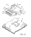
- FIGURE 2 is an isometric view of the card reader of Figure 1 exploded from the circuit board and with the card removed and illustrating components mounted to the board beneath the card reader.
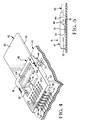
- FIGURE 3 is an isometric view of the board mounting face of the card reader of Figure 1 having a card partially inserted therein.
- FIGURE 4 is an isometric view similar to Figure 1 with the card partially inserted into the reader and illustrating the position of the components mounted on the circuit board.
- FIGURE 5 is a side view of the card reader of Figure 1.
- card reader 10 includes a housing 12 having a top wall 14, a bottom or board mounting face 22, a card-receiving face 26, a rear face or wall 30, and opposed side walls 34, together defining a card-receiving slot 40 and an array of terminals 50.
- Top wall 14 includes a plurality of slots 16 that provide clearance for the terminals 50 when they engage pads 64 of the card 60.
- An enlarged opening 18 remote from the terminals 50 extends through the top wall 14 and is aligned with a corresponding opening beneath the card-receiving slot 40.
- opening 18 permits access to the surface 72 of the circuit board 70 to permit placement of various components 76 on the board, as shown in Figures 2 and 4.
- Rear wall 30 includes a plurality of terminal-receiving passageways 32 in which are disposed the terminals 50.
- Side walls 34 include inwardly directed portions 36 at the lower edges thereof defining card-receiving rails 38 along portions of the side walls 34 dimensioned to receive side edges 66 of a card 60 inserted into the card receiving cavity 40, as shown in Figure 3.
- Card-receiving cavity 40 includes an inner end 42 which defines a card stop surface.
- Side walls 34 further include hold-down receiving slots 46 for receiving hold-downs 48 and stand-off portions 44 proximate card-receiving face 26.
- the rear wall 30 and stand-off portions 44 are elongated to provide a selected distance between the circuit board surface 72 and the card-receiving slot 40 such that low profile electronic components 76 may be mounted to the circuit board and not interfere with the operation of the card 60 being inserted or withdrawn from the card reader 10.
- Terminals 50 include body portions 52.
- surface 72 of circuit board 70 includes a plurality of contact pads 74 for engaging respective board connecting sections 54 of card reader 10 and a plurality of contact pads (not shown) to which components 76 can be mounted.
- the card reader 10 is first positioned on circuit board 70 by means of solder paste, or the like (not shown), and the low profile electronic components are then mounted to board 70 through the opening 18. This allows the manufacturer to position the components and the card reader at optimum locations.
- the board with the components and the card reader thereon can then be soldered by means of infrared, or other techniques, as known in the art to cause the solder to flow to electrically and mechanically secure the card reader 10 and the components 76 to the circuit board 70.
- solder also includes conductive adhesives or other materials used to electrically connect electrical devices to boards. Additionally, the electronic components may have leads that are to be secured by solder or the like in through holes of the board by solder reflow techniques. The hold-downs 48 may be soldered to pads 75 or, alternatively, attached by mechanical means to the board 70.
- the present invention provides an advantage of minimizing the size of the circuit board 70 thereby permitting the electronic apparatus, such as, a cellular telephone or pager to be made considerably smaller.
Landscapes
- Engineering & Computer Science (AREA)
- Artificial Intelligence (AREA)
- Computer Vision & Pattern Recognition (AREA)
- Physics & Mathematics (AREA)
- General Physics & Mathematics (AREA)
- Theoretical Computer Science (AREA)
- Slot Machines And Peripheral Devices (AREA)
- Coupling Device And Connection With Printed Circuit (AREA)
- Credit Cards Or The Like (AREA)
Applications Claiming Priority (2)
| Application Number | Priority Date | Filing Date | Title |
|---|---|---|---|
| US7561498P | 1998-02-20 | 1998-02-20 | |
| US75614P | 1998-02-20 |
Publications (2)
| Publication Number | Publication Date |
|---|---|
| EP0950975A2 true EP0950975A2 (de) | 1999-10-20 |
| EP0950975A3 EP0950975A3 (de) | 2000-02-02 |
Family
ID=22126922
Family Applications (1)
| Application Number | Title | Priority Date | Filing Date |
|---|---|---|---|
| EP99301227A Withdrawn EP0950975A3 (de) | 1998-02-20 | 1999-02-19 | Kartenleser |
Country Status (1)
| Country | Link |
|---|---|
| EP (1) | EP0950975A3 (de) |
Cited By (4)
| Publication number | Priority date | Publication date | Assignee | Title |
|---|---|---|---|---|
| EP1104907A1 (de) * | 1999-11-23 | 2001-06-06 | Molex Incorporated | Kartenleser für die Montage auf einer Leiterplatte |
| EP1168228A3 (de) * | 2000-06-28 | 2002-08-21 | Berg Electronics Manufacturing B.V. | Verbinder für elektronische Karte |
| EP1291805A3 (de) * | 2001-08-31 | 2004-01-21 | Mitsumi Electric Company Ltd. | Verbinder für Speicherkarte |
| GB2405249A (en) * | 2003-08-22 | 2005-02-23 | Ipwireless Inc | Holder for electronic module |
Family Cites Families (3)
| Publication number | Priority date | Publication date | Assignee | Title |
|---|---|---|---|---|
| JP2603509Y2 (ja) * | 1992-12-28 | 2000-03-15 | 日本エー・エム・ピー株式会社 | カードエッジコネクタ |
| US5709568A (en) * | 1995-07-18 | 1998-01-20 | Hon Hai Precision Ind. Co., Ltd. | Connection device for use with memory card connector apparatus |
| DE29721637U1 (de) * | 1997-11-25 | 1998-02-05 | Thomas & Betts Corp | Gerät zum Lesen von Chipkarten |
-
1999
- 1999-02-19 EP EP99301227A patent/EP0950975A3/de not_active Withdrawn
Cited By (6)
| Publication number | Priority date | Publication date | Assignee | Title |
|---|---|---|---|---|
| EP1104907A1 (de) * | 1999-11-23 | 2001-06-06 | Molex Incorporated | Kartenleser für die Montage auf einer Leiterplatte |
| EP1168228A3 (de) * | 2000-06-28 | 2002-08-21 | Berg Electronics Manufacturing B.V. | Verbinder für elektronische Karte |
| EP1291805A3 (de) * | 2001-08-31 | 2004-01-21 | Mitsumi Electric Company Ltd. | Verbinder für Speicherkarte |
| US6733340B2 (en) | 2001-08-31 | 2004-05-11 | Mitsumi Electric Co., Ltd. | Connector for memory card |
| GB2405249A (en) * | 2003-08-22 | 2005-02-23 | Ipwireless Inc | Holder for electronic module |
| GB2405249B (en) * | 2003-08-22 | 2007-03-07 | Ipwireless Inc | Holder for module and method therefor |
Also Published As
| Publication number | Publication date |
|---|---|
| EP0950975A3 (de) | 2000-02-02 |
Similar Documents
| Publication | Publication Date | Title |
|---|---|---|
| US6293464B1 (en) | Card reader | |
| US6641441B2 (en) | Electronic card connector having improved assembly | |
| EP1065754B1 (de) | Oberflächenmontierter elektrischer Verbinder | |
| US6027381A (en) | Insert molded compression connector | |
| JP3216050B2 (ja) | 低背型表面取付電気コネクタ | |
| US6835100B1 (en) | Multi-in-one connector structure | |
| KR20020000001U (ko) | 향상된 접지 단자를 갖는 카드 커넥터 | |
| EP0908978A3 (de) | Kartensteckverbinderanordnung | |
| US7422445B2 (en) | Sinking electrical card connector | |
| US6592408B2 (en) | Sink-type audio socket connector having improved grounding structure | |
| DE69318651D1 (de) | Verbinderblock | |
| US7341461B1 (en) | Memory card adapter | |
| EP0883855A1 (de) | Vorrichtung zur elektrischen verbindung einer chip-karte mit einer leiterplatte | |
| US20060116027A1 (en) | Electrical card connector with improved contact structure | |
| US20090137136A1 (en) | Housing, Terminal and Connector Using Housing and Terminal | |
| KR19990036995A (ko) | 향상된 접지 단자를 갖는 카드 커넥터 | |
| US6011517A (en) | Supporting and holding device for strip metal RF antenna | |
| US6659802B1 (en) | Card connector having control IC therein | |
| EP0729622A1 (de) | Ic-karte mit trägereinstellungsmitteln | |
| EP1104907A1 (de) | Kartenleser für die Montage auf einer Leiterplatte | |
| JP2005032446A (ja) | スモールカードコネクタ | |
| KR100467975B1 (ko) | 지에스엠 이동통신 단말기의 심카드 장착 구조 | |
| KR0129250Y1 (ko) | 콘넥터 | |
| KR200227761Y1 (ko) | 커넥터 어셈블리 구조 | |
| JPH02273475A (ja) | プリント基板カードエッジコネクタ装置 |
Legal Events
| Date | Code | Title | Description |
|---|---|---|---|
| PUAI | Public reference made under article 153(3) epc to a published international application that has entered the european phase |
Free format text: ORIGINAL CODE: 0009012 |
|
| AK | Designated contracting states |
Kind code of ref document: A2 Designated state(s): DE FR GB |
|
| AX | Request for extension of the european patent |
Free format text: AL;LT;LV;MK;RO;SI |
|
| PUAL | Search report despatched |
Free format text: ORIGINAL CODE: 0009013 |
|
| RIN1 | Information on inventor provided before grant (corrected) |
Inventor name: SMALLY, JARED J, JR. |
|
| AK | Designated contracting states |
Kind code of ref document: A3 Designated state(s): AT BE CH CY DE DK ES FI FR GB GR IE IT LI LU MC NL PT SE |
|
| AX | Request for extension of the european patent |
Free format text: AL;LT;LV;MK;RO;SI |
|
| 17P | Request for examination filed |
Effective date: 20000801 |
|
| AKX | Designation fees paid |
Free format text: DE FR GB |
|
| STAA | Information on the status of an ep patent application or granted ep patent |
Free format text: STATUS: THE APPLICATION IS DEEMED TO BE WITHDRAWN |
|
| 18D | Application deemed to be withdrawn |
Effective date: 20060613 |